

Page 1

User’s Guide
Agilent Technologies
E4428C/38C ESG Signal Generators
This guide applies to the following signal generator models:
E4428C ESG Analog Signal Generator
E4438C ESG Vector Signal Generator
Due to our continuing efforts to improve our products through firmware and hardware revisions, signal
generator design and operation may vary from descriptions in this guide. We recommend that you use the
latest revision of this guide to ensure you have up-to-date product information. Compare the print date of this
guide (see bottom of page) with the latest revision, which can be downloaded from the following website:
http://www.agilent.com/find/esg
Manufacturing Part Number: E4400-90503
Printed in USA
July 2007
© Copyright 2001-2007 Agilent Technologies, Inc.
Page 2

Notice
The material contained in this document is provided “as is”, and is subject to being changed, without no tice,
in future editions.
Further, to the maximum extent permitted by applicable law, Agilent disclaims all warranties , either
expressed or implied with regard to this manual and to any of the Agilent products to which it pertains,
including but not limited to the implied warranties of merchantability and fitn ess f or a particular purpose.
Agilent shall not be liable for errors or for incidental or consequential damages in connection with the
furnishing, use, or perfor mance of th is do cumen t or any of the Agilent products to which it pertains. Should
Agilent have a written contract with the User and should any of the contract terms conflict with these terms,
the contract terms shall control.
ii
Page 3

Contents
1. E4428C Analog Signal Generator Overview . . . . . . . . . . . . . . . . . . . . . . . . . . . . . . . . . . . . . . . . . . 1
Standard Analog Signal Generator Features. . . . . . . . . . . . . . . . . . . . . . . . . . . . . . . . . . . . . . . . . . . . .2
Options . . . . . . . . . . . . . . . . . . . . . . . . . . . . . . . . . . . . . . . . . . . . . . . . . . . . . . . . . . . . . . . . . . . . . . . . .3
Firmware Upgrades. . . . . . . . . . . . . . . . . . . . . . . . . . . . . . . . . . . . . . . . . . . . . . . . . . . . . . . . . . . . . . . .3
To Upgrade Firmware . . . . . . . . . . . . . . . . . . . . . . . . . . . . . . . . . . . . . . . . . . . . . . . . . . . . . . . . . . . .3
Calibration . . . . . . . . . . . . . . . . . . . . . . . . . . . . . . . . . . . . . . . . . . . . . . . . . . . . . . . . . . . . . . . . . . . . . .4
Modes of Operation . . . . . . . . . . . . . . . . . . . . . . . . . . . . . . . . . . . . . . . . . . . . . . . . . . . . . . . . . . . . . . .5
Continuous Wave . . . . . . . . . . . . . . . . . . . . . . . . . . . . . . . . . . . . . . . . . . . . . . . . . . . . . . . . . . . . . . .5
Swept Signal . . . . . . . . . . . . . . . . . . . . . . . . . . . . . . . . . . . . . . . . . . . . . . . . . . . . . . . . . . . . . . . . . . .5
Analog Modulation . . . . . . . . . . . . . . . . . . . . . . . . . . . . . . . . . . . . . . . . . . . . . . . . . . . . . . . . . . . . . .5
Front Panel Overview. . . . . . . . . . . . . . . . . . . . . . . . . . . . . . . . . . . . . . . . . . . . . . . . . . . . . . . . . . . . . .6
1. Display . . . . . . . . . . . . . . . . . . . . . . . . . . . . . . . . . . . . . . . . . . . . . . . . . . . . . . . . . . . . . . . . . . . . .6
2. Softkeys. . . . . . . . . . . . . . . . . . . . . . . . . . . . . . . . . . . . . . . . . . . . . . . . . . . . . . . . . . . . . . . . . . . . .6
3. Frequency Key . . . . . . . . . . . . . . . . . . . . . . . . . . . . . . . . . . . . . . . . . . . . . . . . . . . . . . . . . . . . . . .7
4. Amplitude Key . . . . . . . . . . . . . . . . . . . . . . . . . . . . . . . . . . . . . . . . . . . . . . . . . . . . . . . . . . . . . . .7
5. Knob . . . . . . . . . . . . . . . . . . . . . . . . . . . . . . . . . . . . . . . . . . . . . . . . . . . . . . . . . . . . . . . . . . . . . . .7
7. Save Key . . . . . . . . . . . . . . . . . . . . . . . . . . . . . . . . . . . . . . . . . . . . . . . . . . . . . . . . . . . . . . . . . . . .7
7. Menu Keys . . . . . . . . . . . . . . . . . . . . . . . . . . . . . . . . . . . . . . . . . . . . . . . . . . . . . . . . . . . . . . . . . .7
8. Recall Key. . . . . . . . . . . . . . . . . . . . . . . . . . . . . . . . . . . . . . . . . . . . . . . . . . . . . . . . . . . . . . . . . . .7
9. EXT 1 INPUT Connector . . . . . . . . . . . . . . . . . . . . . . . . . . . . . . . . . . . . . . . . . . . . . . . . . . . . . . .8
10. EXT 2 INPUT Connector . . . . . . . . . . . . . . . . . . . . . . . . . . . . . . . . . . . . . . . . . . . . . . . . . . . . . .8
11. Help Key . . . . . . . . . . . . . . . . . . . . . . . . . . . . . . . . . . . . . . . . . . . . . . . . . . . . . . . . . . . . . . . . . . .8
12. Trigger Key. . . . . . . . . . . . . . . . . . . . . . . . . . . . . . . . . . . . . . . . . . . . . . . . . . . . . . . . . . . . . . . . .8
13. LF OUTPUT Connector . . . . . . . . . . . . . . . . . . . . . . . . . . . . . . . . . . . . . . . . . . . . . . . . . . . . . . .8
14. RF OUTPUT Connector . . . . . . . . . . . . . . . . . . . . . . . . . . . . . . . . . . . . . . . . . . . . . . . . . . . . . . .9
15. Mod On/Off Key . . . . . . . . . . . . . . . . . . . . . . . . . . . . . . . . . . . . . . . . . . . . . . . . . . . . . . . . . . . .9
16. RF On/Off Key . . . . . . . . . . . . . . . . . . . . . . . . . . . . . . . . . . . . . . . . . . . . . . . . . . . . . . . . . . . . . .9
17. Numeric Keypad . . . . . . . . . . . . . . . . . . . . . . . . . . . . . . . . . . . . . . . . . . . . . . . . . . . . . . . . . . . . .9
18. Incr Set Key. . . . . . . . . . . . . . . . . . . . . . . . . . . . . . . . . . . . . . . . . . . . . . . . . . . . . . . . . . . . . . . . .9
19. Arrow Keys. . . . . . . . . . . . . . . . . . . . . . . . . . . . . . . . . . . . . . . . . . . . . . . . . . . . . . . . . . . . . . . .10
20. Hold Key. . . . . . . . . . . . . . . . . . . . . . . . . . . . . . . . . . . . . . . . . . . . . . . . . . . . . . . . . . . . . . . . . .10
21. Return Key . . . . . . . . . . . . . . . . . . . . . . . . . . . . . . . . . . . . . . . . . . . . . . . . . . . . . . . . . . . . . . . .10
22. Display Contrast Increase Key . . . . . . . . . . . . . . . . . . . . . . . . . . . . . . . . . . . . . . . . . . . . . . . . .10
23. Display Contrast Decrease Key. . . . . . . . . . . . . . . . . . . . . . . . . . . . . . . . . . . . . . . . . . . . . . . . .10
24. Local Key . . . . . . . . . . . . . . . . . . . . . . . . . . . . . . . . . . . . . . . . . . . . . . . . . . . . . . . . . . . . . . . . .10
25. Preset Key . . . . . . . . . . . . . . . . . . . . . . . . . . . . . . . . . . . . . . . . . . . . . . . . . . . . . . . . . . . . . . . . .10
26. Standby LED. . . . . . . . . . . . . . . . . . . . . . . . . . . . . . . . . . . . . . . . . . . . . . . . . . . . . . . . . . . . . . .10
27. Line Power LED . . . . . . . . . . . . . . . . . . . . . . . . . . . . . . . . . . . . . . . . . . . . . . . . . . . . . . . . . . . .10
iii
Page 4

Contents
28. Power Switch . . . . . . . . . . . . . . . . . . . . . . . . . . . . . . . . . . . . . . . . . . . . . . . . . . . . . . . . . . . . . .11
Front Panel Display . . . . . . . . . . . . . . . . . . . . . . . . . . . . . . . . . . . . . . . . . . . . . . . . . . . . . . . . . . . . . . 12
1. Frequency Area. . . . . . . . . . . . . . . . . . . . . . . . . . . . . . . . . . . . . . . . . . . . . . . . . . . . . . . . . . . . . . 12
2. Annunciators. . . . . . . . . . . . . . . . . . . . . . . . . . . . . . . . . . . . . . . . . . . . . . . . . . . . . . . . . . . . . . . .13
3. Amplitude Area. . . . . . . . . . . . . . . . . . . . . . . . . . . . . . . . . . . . . . . . . . . . . . . . . . . . . . . . . . . . . .15
4. Softkey Label Area. . . . . . . . . . . . . . . . . . . . . . . . . . . . . . . . . . . . . . . . . . . . . . . . . . . . . . . . . . . 15
5. Error Message Area . . . . . . . . . . . . . . . . . . . . . . . . . . . . . . . . . . . . . . . . . . . . . . . . . . . . . . . . . .15
6. Text Area . . . . . . . . . . . . . . . . . . . . . . . . . . . . . . . . . . . . . . . . . . . . . . . . . . . . . . . . . . . . . . . . . . . 15
7. Active Function Area . . . . . . . . . . . . . . . . . . . . . . . . . . . . . . . . . . . . . . . . . . . . . . . . . . . . . . . . .15
Rear Panel Overview . . . . . . . . . . . . . . . . . . . . . . . . . . . . . . . . . . . . . . . . . . . . . . . . . . . . . . . . . . . . . 16
1. AC Power Receptacle. . . . . . . . . . . . . . . . . . . . . . . . . . . . . . . . . . . . . . . . . . . . . . . . . . . . . . . . .17
2. GPIB Connector . . . . . . . . . . . . . . . . . . . . . . . . . . . . . . . . . . . . . . . . . . . . . . . . . . . . . . . . . . . . .17
3. RS 232 Connector. . . . . . . . . . . . . . . . . . . . . . . . . . . . . . . . . . . . . . . . . . . . . . . . . . . . . . . . . . . . 17
4. LAN Connector. . . . . . . . . . . . . . . . . . . . . . . . . . . . . . . . . . . . . . . . . . . . . . . . . . . . . . . . . . . . . .18
5. TRIG OUT Connector . . . . . . . . . . . . . . . . . . . . . . . . . . . . . . . . . . . . . . . . . . . . . . . . . . . . . . . .18
6. TRIG IN Connector . . . . . . . . . . . . . . . . . . . . . . . . . . . . . . . . . . . . . . . . . . . . . . . . . . . . . . . . . .18
7. 10 MHz IN Connector . . . . . . . . . . . . . . . . . . . . . . . . . . . . . . . . . . . . . . . . . . . . . . . . . . . . . . . . 18
8. SWEEP OUT Connector . . . . . . . . . . . . . . . . . . . . . . . . . . . . . . . . . . . . . . . . . . . . . . . . . . . . . .18
9. 10 MHz OUT Connector . . . . . . . . . . . . . . . . . . . . . . . . . . . . . . . . . . . . . . . . . . . . . . . . . . . . . . 18
2. E4438C Vector Signal Generator Overview. . . . . . . . . . . . . . . . . . . . . . . . . . . . . . . . . . . . . . . . . . . 19
Standard Vector Signal Generator Features . . . . . . . . . . . . . . . . . . . . . . . . . . . . . . . . . . . . . . . . . . . .20
Options . . . . . . . . . . . . . . . . . . . . . . . . . . . . . . . . . . . . . . . . . . . . . . . . . . . . . . . . . . . . . . . . . . . . . . . .21
Understanding Baseband Generator Options . . . . . . . . . . . . . . . . . . . . . . . . . . . . . . . . . . . . . . . . .21
Firmware Upgrades . . . . . . . . . . . . . . . . . . . . . . . . . . . . . . . . . . . . . . . . . . . . . . . . . . . . . . . . . . . . . .22
To Upgrade Firmware. . . . . . . . . . . . . . . . . . . . . . . . . . . . . . . . . . . . . . . . . . . . . . . . . . . . . . . . . . .22
Calibration . . . . . . . . . . . . . . . . . . . . . . . . . . . . . . . . . . . . . . . . . . . . . . . . . . . . . . . . . . . . . . . . . . . . . 23
Modes of Operation . . . . . . . . . . . . . . . . . . . . . . . . . . . . . . . . . . . . . . . . . . . . . . . . . . . . . . . . . . . . . . 24
Continuous Wave . . . . . . . . . . . . . . . . . . . . . . . . . . . . . . . . . . . . . . . . . . . . . . . . . . . . . . . . . . . . . . 24
Swept Signal. . . . . . . . . . . . . . . . . . . . . . . . . . . . . . . . . . . . . . . . . . . . . . . . . . . . . . . . . . . . . . . . . .24
Analog Modulation. . . . . . . . . . . . . . . . . . . . . . . . . . . . . . . . . . . . . . . . . . . . . . . . . . . . . . . . . . . . . 24
Digital Modulation . . . . . . . . . . . . . . . . . . . . . . . . . . . . . . . . . . . . . . . . . . . . . . . . . . . . . . . . . . . . . 24
Front Panel Overview. . . . . . . . . . . . . . . . . . . . . . . . . . . . . . . . . . . . . . . . . . . . . . . . . . . . . . . . . . . . . 26
1. Display . . . . . . . . . . . . . . . . . . . . . . . . . . . . . . . . . . . . . . . . . . . . . . . . . . . . . . . . . . . . . . . . . . . .26
2. Softkeys . . . . . . . . . . . . . . . . . . . . . . . . . . . . . . . . . . . . . . . . . . . . . . . . . . . . . . . . . . . . . . . . . . . 26
3. Frequency Key . . . . . . . . . . . . . . . . . . . . . . . . . . . . . . . . . . . . . . . . . . . . . . . . . . . . . . . . . . . . . .26
4. Amplitude Key . . . . . . . . . . . . . . . . . . . . . . . . . . . . . . . . . . . . . . . . . . . . . . . . . . . . . . . . . . . . . .27
5. Knob . . . . . . . . . . . . . . . . . . . . . . . . . . . . . . . . . . . . . . . . . . . . . . . . . . . . . . . . . . . . . . . . . . . . . .27
iv
Page 5

Contents
6. Menu Keys . . . . . . . . . . . . . . . . . . . . . . . . . . . . . . . . . . . . . . . . . . . . . . . . . . . . . . . . . . . . . . . . .27
7. Save Key . . . . . . . . . . . . . . . . . . . . . . . . . . . . . . . . . . . . . . . . . . . . . . . . . . . . . . . . . . . . . . . . . . .27
8. Recall Key. . . . . . . . . . . . . . . . . . . . . . . . . . . . . . . . . . . . . . . . . . . . . . . . . . . . . . . . . . . . . . . . . . 27
9. EXT 1 INPUT Connector . . . . . . . . . . . . . . . . . . . . . . . . . . . . . . . . . . . . . . . . . . . . . . . . . . . . . .28
10. EXT 2 INPUT Connector . . . . . . . . . . . . . . . . . . . . . . . . . . . . . . . . . . . . . . . . . . . . . . . . . . . . .28
11. Help Key . . . . . . . . . . . . . . . . . . . . . . . . . . . . . . . . . . . . . . . . . . . . . . . . . . . . . . . . . . . . . . . . . .28
12. Trigger Key. . . . . . . . . . . . . . . . . . . . . . . . . . . . . . . . . . . . . . . . . . . . . . . . . . . . . . . . . . . . . . . .28
13. LF OUTPUT Connector . . . . . . . . . . . . . . . . . . . . . . . . . . . . . . . . . . . . . . . . . . . . . . . . . . . . . .29
14. RF OUTPUT Connector . . . . . . . . . . . . . . . . . . . . . . . . . . . . . . . . . . . . . . . . . . . . . . . . . . . . . .29
15. Mod On/Off Key . . . . . . . . . . . . . . . . . . . . . . . . . . . . . . . . . . . . . . . . . . . . . . . . . . . . . . . . . . .29
16. RF On/Off Key . . . . . . . . . . . . . . . . . . . . . . . . . . . . . . . . . . . . . . . . . . . . . . . . . . . . . . . . . . . . .29
17. Numeric Keypad . . . . . . . . . . . . . . . . . . . . . . . . . . . . . . . . . . . . . . . . . . . . . . . . . . . . . . . . . . . .29
18. Incr Set Key. . . . . . . . . . . . . . . . . . . . . . . . . . . . . . . . . . . . . . . . . . . . . . . . . . . . . . . . . . . . . . . .30
19. Arrow Keys. . . . . . . . . . . . . . . . . . . . . . . . . . . . . . . . . . . . . . . . . . . . . . . . . . . . . . . . . . . . . . . .30
20. Hold Key. . . . . . . . . . . . . . . . . . . . . . . . . . . . . . . . . . . . . . . . . . . . . . . . . . . . . . . . . . . . . . . . . .30
21. Return Key . . . . . . . . . . . . . . . . . . . . . . . . . . . . . . . . . . . . . . . . . . . . . . . . . . . . . . . . . . . . . . . .30
22. Display Contrast Increase Key . . . . . . . . . . . . . . . . . . . . . . . . . . . . . . . . . . . . . . . . . . . . . . . . .30
23. Display Contrast Decrease Key. . . . . . . . . . . . . . . . . . . . . . . . . . . . . . . . . . . . . . . . . . . . . . . . .30
24. Local Key . . . . . . . . . . . . . . . . . . . . . . . . . . . . . . . . . . . . . . . . . . . . . . . . . . . . . . . . . . . . . . . . .30
25. Preset Key . . . . . . . . . . . . . . . . . . . . . . . . . . . . . . . . . . . . . . . . . . . . . . . . . . . . . . . . . . . . . . . . .30
26. Standby LED. . . . . . . . . . . . . . . . . . . . . . . . . . . . . . . . . . . . . . . . . . . . . . . . . . . . . . . . . . . . . . .31
27. Line Power LED . . . . . . . . . . . . . . . . . . . . . . . . . . . . . . . . . . . . . . . . . . . . . . . . . . . . . . . . . . . .31
28. Power Switch. . . . . . . . . . . . . . . . . . . . . . . . . . . . . . . . . . . . . . . . . . . . . . . . . . . . . . . . . . . . . . .31
29. SYMBOL SYNC Connector (Option 001/601 or 002/602) . . . . . . . . . . . . . . . . . . . . . . . . . . .31
30. DATA CLOCK Connector (Option 001/601 or 002/602). . . . . . . . . . . . . . . . . . . . . . . . . . . . .31
31. DATA Connector (Option 001/601 or 002/602) . . . . . . . . . . . . . . . . . . . . . . . . . . . . . . . . . . . .32
32. Q Connector . . . . . . . . . . . . . . . . . . . . . . . . . . . . . . . . . . . . . . . . . . . . . . . . . . . . . . . . . . . . . . . 32
33. I Connector . . . . . . . . . . . . . . . . . . . . . . . . . . . . . . . . . . . . . . . . . . . . . . . . . . . . . . . . . . . . . . . .32
Front Panel Display . . . . . . . . . . . . . . . . . . . . . . . . . . . . . . . . . . . . . . . . . . . . . . . . . . . . . . . . . . . . . .33
1. Frequency Area. . . . . . . . . . . . . . . . . . . . . . . . . . . . . . . . . . . . . . . . . . . . . . . . . . . . . . . . . . . . . .33
2. Annunciators. . . . . . . . . . . . . . . . . . . . . . . . . . . . . . . . . . . . . . . . . . . . . . . . . . . . . . . . . . . . . . . .34
3. Digital Modulation Annunciators . . . . . . . . . . . . . . . . . . . . . . . . . . . . . . . . . . . . . . . . . . . . . . . .36
4. Amplitude Area. . . . . . . . . . . . . . . . . . . . . . . . . . . . . . . . . . . . . . . . . . . . . . . . . . . . . . . . . . . . . .36
5. Softkey Label Area . . . . . . . . . . . . . . . . . . . . . . . . . . . . . . . . . . . . . . . . . . . . . . . . . . . . . . . . . . .36
6. Error Message Area. . . . . . . . . . . . . . . . . . . . . . . . . . . . . . . . . . . . . . . . . . . . . . . . . . . . . . . . . . .36
7. Text Area. . . . . . . . . . . . . . . . . . . . . . . . . . . . . . . . . . . . . . . . . . . . . . . . . . . . . . . . . . . . . . . . . . .36
8. Active Function Area . . . . . . . . . . . . . . . . . . . . . . . . . . . . . . . . . . . . . . . . . . . . . . . . . . . . . . . . .36
Rear Panel Overview . . . . . . . . . . . . . . . . . . . . . . . . . . . . . . . . . . . . . . . . . . . . . . . . . . . . . . . . . . . . .37
v
Page 6

Contents
1. 321.4 IN Connector (Option 300). . . . . . . . . . . . . . . . . . . . . . . . . . . . . . . . . . . . . . . . . . . . . . . .38
2. BER GATE IN Connector (Option UN7). . . . . . . . . . . . . . . . . . . . . . . . . . . . . . . . . . . . . . . . . .38
3. BER CLK IN Connector (Option UN7) . . . . . . . . . . . . . . . . . . . . . . . . . . . . . . . . . . . . . . . . . . . 38
4. BER DATA IN Connector (Option UN7). . . . . . . . . . . . . . . . . . . . . . . . . . . . . . . . . . . . . . . . . .38
5. I-bar OUT Connector (Option 001/601 or 002/602) . . . . . . . . . . . . . . . . . . . . . . . . . . . . . . . . .38
6. I OUT Connector (Option 001/601 or 002/602). . . . . . . . . . . . . . . . . . . . . . . . . . . . . . . . . . . . . 39
7. COH CARRIER Output Connector . . . . . . . . . . . . . . . . . . . . . . . . . . . . . . . . . . . . . . . . . . . . . .39
8. Q OUT Connector (Option 001/601 or 002/602) . . . . . . . . . . . . . . . . . . . . . . . . . . . . . . . . . . . .39
9. Q-bar OUT Connector (Option 001/601 or 002/602). . . . . . . . . . . . . . . . . . . . . . . . . . . . . . . . . 40
10. EVENT 1 Connector (Option 001/601 or 002/602) . . . . . . . . . . . . . . . . . . . . . . . . . . . . . . . . . 40
11. EVENT 2 Connector (Option 001/601 or 002/602) . . . . . . . . . . . . . . . . . . . . . . . . . . . . . . . . . 40
12. PATT TRIG IN Connector (Option 001/601 or 002/602). . . . . . . . . . . . . . . . . . . . . . . . . . . . . 41
13. AUX I/O Connector . . . . . . . . . . . . . . . . . . . . . . . . . . . . . . . . . . . . . . . . . . . . . . . . . . . . . . . . . 41
14. DIGITAL BUS . . . . . . . . . . . . . . . . . . . . . . . . . . . . . . . . . . . . . . . . . . . . . . . . . . . . . . . . . . . . .43
15. AC Power Receptacle. . . . . . . . . . . . . . . . . . . . . . . . . . . . . . . . . . . . . . . . . . . . . . . . . . . . . . . .43
16. GPIB Connector . . . . . . . . . . . . . . . . . . . . . . . . . . . . . . . . . . . . . . . . . . . . . . . . . . . . . . . . . . . .44
17. RS 232 Connector. . . . . . . . . . . . . . . . . . . . . . . . . . . . . . . . . . . . . . . . . . . . . . . . . . . . . . . . . . . 44
18. LAN Connector. . . . . . . . . . . . . . . . . . . . . . . . . . . . . . . . . . . . . . . . . . . . . . . . . . . . . . . . . . . . .44
19. TRIG OUT Connector . . . . . . . . . . . . . . . . . . . . . . . . . . . . . . . . . . . . . . . . . . . . . . . . . . . . . . . 45
20. BURST GATE IN Connector (Option 001/601 or 002/602) . . . . . . . . . . . . . . . . . . . . . . . . . . 45
21. TRIG IN Connector . . . . . . . . . . . . . . . . . . . . . . . . . . . . . . . . . . . . . . . . . . . . . . . . . . . . . . . . .45
22. 10 MHz IN Connector . . . . . . . . . . . . . . . . . . . . . . . . . . . . . . . . . . . . . . . . . . . . . . . . . . . . . . . 45
23. SWEEP OUT Connector . . . . . . . . . . . . . . . . . . . . . . . . . . . . . . . . . . . . . . . . . . . . . . . . . . . . .45
24. 10 MHz OUT Connector . . . . . . . . . . . . . . . . . . . . . . . . . . . . . . . . . . . . . . . . . . . . . . . . . . . . . 46
25. BASEBAND GEN REF IN Connector (Option 001/601 or 002/602). . . . . . . . . . . . . . . . . . . 46
3. Basic Operation . . . . . . . . . . . . . . . . . . . . . . . . . . . . . . . . . . . . . . . . . . . . . . . . . . . . . . . . . . . . . . . . 47
Using Table Editors . . . . . . . . . . . . . . . . . . . . . . . . . . . . . . . . . . . . . . . . . . . . . . . . . . . . . . . . . . . . . .48
Table Editor Softkeys . . . . . . . . . . . . . . . . . . . . . . . . . . . . . . . . . . . . . . . . . . . . . . . . . . . . . . . . . . . 49
Modifying Table Items in the Data Fields . . . . . . . . . . . . . . . . . . . . . . . . . . . . . . . . . . . . . . . . . . .49
Configuring the RF Output. . . . . . . . . . . . . . . . . . . . . . . . . . . . . . . . . . . . . . . . . . . . . . . . . . . . . . . . .50
Configuring a Continuous Wave RF Output. . . . . . . . . . . . . . . . . . . . . . . . . . . . . . . . . . . . . . . . . .50
Configuring a Swept RF Output. . . . . . . . . . . . . . . . . . . . . . . . . . . . . . . . . . . . . . . . . . . . . . . . . . .53
Generating the Modulation Format . . . . . . . . . . . . . . . . . . . . . . . . . . . . . . . . . . . . . . . . . . . . . . . . . .58
Modulating the Carrier Signal . . . . . . . . . . . . . . . . . . . . . . . . . . . . . . . . . . . . . . . . . . . . . . . . . . . . . . 60
To Turn the Modulation On . . . . . . . . . . . . . . . . . . . . . . . . . . . . . . . . . . . . . . . . . . . . . . . . . . . . . . 60
To Turn the Modulation Off . . . . . . . . . . . . . . . . . . . . . . . . . . . . . . . . . . . . . . . . . . . . . . . . . . . . . .60
Creating and Applying User Flatness Correction. . . . . . . . . . . . . . . . . . . . . . . . . . . . . . . . . . . . . . . .61
vi
Page 7

Contents
Creating a User Flatness Correction Array. . . . . . . . . . . . . . . . . . . . . . . . . . . . . . . . . . . . . . . . . . .61
Using the Memory Catalog. . . . . . . . . . . . . . . . . . . . . . . . . . . . . . . . . . . . . . . . . . . . . . . . . . . . . . . . .68
Viewing Stored Files. . . . . . . . . . . . . . . . . . . . . . . . . . . . . . . . . . . . . . . . . . . . . . . . . . . . . . . . . . . .68
Storing Files . . . . . . . . . . . . . . . . . . . . . . . . . . . . . . . . . . . . . . . . . . . . . . . . . . . . . . . . . . . . . . . . . . 69
Using the Instrument State Registers . . . . . . . . . . . . . . . . . . . . . . . . . . . . . . . . . . . . . . . . . . . . . . . . .70
Saving an Instrument State . . . . . . . . . . . . . . . . . . . . . . . . . . . . . . . . . . . . . . . . . . . . . . . . . . . . . . .71
Recalling an Instrument State . . . . . . . . . . . . . . . . . . . . . . . . . . . . . . . . . . . . . . . . . . . . . . . . . . . . .72
Saving an Instrument State for a Waveform File . . . . . . . . . . . . . . . . . . . . . . . . . . . . . . . . . . . . . .72
Recalling an Instrument State for a Waveform File . . . . . . . . . . . . . . . . . . . . . . . . . . . . . . . . . . . .73
Deleting Registers and Sequences. . . . . . . . . . . . . . . . . . . . . . . . . . . . . . . . . . . . . . . . . . . . . . . . . .74
Using Security Functions . . . . . . . . . . . . . . . . . . . . . . . . . . . . . . . . . . . . . . . . . . . . . . . . . . . . . . . . . .75
Understanding Memory Types . . . . . . . . . . . . . . . . . . . . . . . . . . . . . . . . . . . . . . . . . . . . . . . . . . . .75
Removing Sensitive Data from Memory . . . . . . . . . . . . . . . . . . . . . . . . . . . . . . . . . . . . . . . . . . . .78
Using the Secure Display . . . . . . . . . . . . . . . . . . . . . . . . . . . . . . . . . . . . . . . . . . . . . . . . . . . . . . . .82
Enabling Options (E4438C Only). . . . . . . . . . . . . . . . . . . . . . . . . . . . . . . . . . . . . . . . . . . . . . . . . . . .83
Enabling a Software Option . . . . . . . . . . . . . . . . . . . . . . . . . . . . . . . . . . . . . . . . . . . . . . . . . . . . . .83
Waveform Licenses. . . . . . . . . . . . . . . . . . . . . . . . . . . . . . . . . . . . . . . . . . . . . . . . . . . . . . . . . . . . .84
Using the Web Server . . . . . . . . . . . . . . . . . . . . . . . . . . . . . . . . . . . . . . . . . . . . . . . . . . . . . . . . . . . . .85
Activating the Web Server . . . . . . . . . . . . . . . . . . . . . . . . . . . . . . . . . . . . . . . . . . . . . . . . . . . . . . .85
4. Basic Digital Operation. . . . . . . . . . . . . . . . . . . . . . . . . . . . . . . . . . . . . . . . . . . . . . . . . . . . . . . . . . .89
Custom Modulation . . . . . . . . . . . . . . . . . . . . . . . . . . . . . . . . . . . . . . . . . . . . . . . . . . . . . . . . . . . . . .90
Custom Arb Waveform Generator . . . . . . . . . . . . . . . . . . . . . . . . . . . . . . . . . . . . . . . . . . . . . . . . .90
Custom Real Time I/Q Baseband . . . . . . . . . . . . . . . . . . . . . . . . . . . . . . . . . . . . . . . . . . . . . . . . . .91
Arbitrary (ARB) Waveform File Headers. . . . . . . . . . . . . . . . . . . . . . . . . . . . . . . . . . . . . . . . . . . . . .92
Creating a File Header. . . . . . . . . . . . . . . . . . . . . . . . . . . . . . . . . . . . . . . . . . . . . . . . . . . . . . . . . . .92
Modifying Header Information . . . . . . . . . . . . . . . . . . . . . . . . . . . . . . . . . . . . . . . . . . . . . . . . . . .94
Dual ARB Player Waveform Sequence File Headers. . . . . . . . . . . . . . . . . . . . . . . . . . . . . . . . . .100
Editing and Viewing File Headers in the Dual ARB Player. . . . . . . . . . . . . . . . . . . . . . . . . . . . .100
Playing a Waveform File containing a Header . . . . . . . . . . . . . . . . . . . . . . . . . . . . . . . . . . . . . . .104
Using the Dual ARB Waveform Player . . . . . . . . . . . . . . . . . . . . . . . . . . . . . . . . . . . . . . . . . . . . . .106
Accessing the Dual ARB Player. . . . . . . . . . . . . . . . . . . . . . . . . . . . . . . . . . . . . . . . . . . . . . . . . .106
Creating Waveform Segments. . . . . . . . . . . . . . . . . . . . . . . . . . . . . . . . . . . . . . . . . . . . . . . . . . . .107
Creating a Waveform Sequence . . . . . . . . . . . . . . . . . . . . . . . . . . . . . . . . . . . . . . . . . . . . . . . . . .108
Playing a Waveform Sequence . . . . . . . . . . . . . . . . . . . . . . . . . . . . . . . . . . . . . . . . . . . . . . . . . . .109
Editing a Waveform Sequence . . . . . . . . . . . . . . . . . . . . . . . . . . . . . . . . . . . . . . . . . . . . . . . . . . .110
Adding Real-Time Noise to a Dual ARB Waveform (Option 403) . . . . . . . . . . . . . . . . . . . . . . .111
Storing and Loading Waveform Segments . . . . . . . . . . . . . . . . . . . . . . . . . . . . . . . . . . . . . . . . . .112
vii
Page 8

Contents
Using Waveform 5-Pack Licensing (Options 221-229) . . . . . . . . . . . . . . . . . . . . . . . . . . . . . . . .113
Understanding the I/Q Modulator Filter. . . . . . . . . . . . . . . . . . . . . . . . . . . . . . . . . . . . . . . . . . . . . .120
Applying An I/Q Modulator Filter . . . . . . . . . . . . . . . . . . . . . . . . . . . . . . . . . . . . . . . . . . . . . . . .121
Local Settings for ARB Waveform Formats and the Dual ARB Player . . . . . . . . . . . . . . . . . . . . .122
I/Q Attenuator and Filters Settings. . . . . . . . . . . . . . . . . . . . . . . . . . . . . . . . . . . . . . . . . . . . . . . . 122
Waveform Runtime Scaling . . . . . . . . . . . . . . . . . . . . . . . . . . . . . . . . . . . . . . . . . . . . . . . . . . . . .124
High Crest Mode. . . . . . . . . . . . . . . . . . . . . . . . . . . . . . . . . . . . . . . . . . . . . . . . . . . . . . . . . . . . . .124
ARB Sample Clock. . . . . . . . . . . . . . . . . . . . . . . . . . . . . . . . . . . . . . . . . . . . . . . . . . . . . . . . . . . .124
Waveform Markers . . . . . . . . . . . . . . . . . . . . . . . . . . . . . . . . . . . . . . . . . . . . . . . . . . . . . . . . . . . .125
Using Waveform Markers . . . . . . . . . . . . . . . . . . . . . . . . . . . . . . . . . . . . . . . . . . . . . . . . . . . . . . . .129
Waveform Marker Concepts. . . . . . . . . . . . . . . . . . . . . . . . . . . . . . . . . . . . . . . . . . . . . . . . . . . . .130
Accessing Marker Utilities . . . . . . . . . . . . . . . . . . . . . . . . . . . . . . . . . . . . . . . . . . . . . . . . . . . . . .134
Viewing Waveform Segment Markers . . . . . . . . . . . . . . . . . . . . . . . . . . . . . . . . . . . . . . . . . . . . .135
Clearing Marker Points from a Waveform Segment. . . . . . . . . . . . . . . . . . . . . . . . . . . . . . . . . . .136
Setting Marker Points in a Waveform Segment . . . . . . . . . . . . . . . . . . . . . . . . . . . . . . . . . . . . . . 137
Controlling Markers in a Waveform Sequence (Dual ARB Only). . . . . . . . . . . . . . . . . . . . . . . .1 39
Viewing a Marker Pulse . . . . . . . . . . . . . . . . . . . . . . . . . . . . . . . . . . . . . . . . . . . . . . . . . . . . . . . . 141
Using the RF Blanking Marker Function . . . . . . . . . . . . . . . . . . . . . . . . . . . . . . . . . . . . . . . . . . .142
Setting Marker Polarity. . . . . . . . . . . . . . . . . . . . . . . . . . . . . . . . . . . . . . . . . . . . . . . . . . . . . . . . . 144
Triggering Waveforms . . . . . . . . . . . . . . . . . . . . . . . . . . . . . . . . . . . . . . . . . . . . . . . . . . . . . . . . . . . 145
Source . . . . . . . . . . . . . . . . . . . . . . . . . . . . . . . . . . . . . . . . . . . . . . . . . . . . . . . . . . . . . . . . . . . . . .146
Mode and Response . . . . . . . . . . . . . . . . . . . . . . . . . . . . . . . . . . . . . . . . . . . . . . . . . . . . . . . . . . . 146
Accessing Trigger Utilities. . . . . . . . . . . . . . . . . . . . . . . . . . . . . . . . . . . . . . . . . . . . . . . . . . . . . . 147
Setting the Polarity of an External Trigger. . . . . . . . . . . . . . . . . . . . . . . . . . . . . . . . . . . . . . . . . .148
Using Gated Triggering . . . . . . . . . . . . . . . . . . . . . . . . . . . . . . . . . . . . . . . . . . . . . . . . . . . . . . . .148
Using Segment Advance Triggering. . . . . . . . . . . . . . . . . . . . . . . . . . . . . . . . . . . . . . . . . . . . . . .150
Using External Triggering . . . . . . . . . . . . . . . . . . . . . . . . . . . . . . . . . . . . . . . . . . . . . . . . . . . . . .151
Using Waveform Clipping . . . . . . . . . . . . . . . . . . . . . . . . . . . . . . . . . . . . . . . . . . . . . . . . . . . . . . . . 154
How Power Peaks Develop. . . . . . . . . . . . . . . . . . . . . . . . . . . . . . . . . . . . . . . . . . . . . . . . . . . . . . 154
How Peaks Cause Spectral Regrowth. . . . . . . . . . . . . . . . . . . . . . . . . . . . . . . . . . . . . . . . . . . . . .156
How Clipping Reduces Peak-to-Average Power . . . . . . . . . . . . . . . . . . . . . . . . . . . . . . . . . . . . .157
Configuring Circular Clipping . . . . . . . . . . . . . . . . . . . . . . . . . . . . . . . . . . . . . . . . . . . . . . . . . . . 160
Configuring Rectangular Clipping . . . . . . . . . . . . . . . . . . . . . . . . . . . . . . . . . . . . . . . . . . . . . . . .161
Using Waveform Scaling . . . . . . . . . . . . . . . . . . . . . . . . . . . . . . . . . . . . . . . . . . . . . . . . . . . . . . . . .162
How DAC Over-Range Errors Occur . . . . . . . . . . . . . . . . . . . . . . . . . . . . . . . . . . . . . . . . . . . . . .162
How Scaling Eliminates DAC Over-Range Errors. . . . . . . . . . . . . . . . . . . . . . . . . . . . . . . . . . . .163
Scaling a Currently Playing Waveform (Runtime Scaling) . . . . . . . . . . . . . . . . . . . . . . . . . . . . .164
Scaling a Waveform File in Volatile Memory . . . . . . . . . . . . . . . . . . . . . . . . . . . . . . . . . . . . . . . 165
viii
Page 9

Contents
Using Customized Burst Shape Curves . . . . . . . . . . . . . . . . . . . . . . . . . . . . . . . . . . . . . . . . . . . . . .166
Understanding Burst Shape. . . . . . . . . . . . . . . . . . . . . . . . . . . . . . . . . . . . . . . . . . . . . . . . . . . . . .166
Creating a User-Defined Burst Shape Curve . . . . . . . . . . . . . . . . . . . . . . . . . . . . . . . . . . . . . . . .168
Storing a User-Defined Burst Shape Curve . . . . . . . . . . . . . . . . . . . . . . . . . . . . . . . . . . . . . . . . .171
Recalling a User-Defined Burst Shape Curve. . . . . . . . . . . . . . . . . . . . . . . . . . . . . . . . . . . . . . . .171
Generating the Waveform . . . . . . . . . . . . . . . . . . . . . . . . . . . . . . . . . . . . . . . . . . . . . . . . . . . . . . .172
Configuring the RF Output . . . . . . . . . . . . . . . . . . . . . . . . . . . . . . . . . . . . . . . . . . . . . . . . . . . . . .172
Using Finite Impulse Response (FIR) Filters. . . . . . . . . . . . . . . . . . . . . . . . . . . . . . . . . . . . . . . . . .173
Creating a User-Defined FIR Filter Using the FIR Table Editor . . . . . . . . . . . . . . . . . . . . . . . . .173
Modifying a FIR Filter Using the FIR Table Editor. . . . . . . . . . . . . . . . . . . . . . . . . . . . . . . . . . . . .178
Loading the Default Gaussian FIR File. . . . . . . . . . . . . . . . . . . . . . . . . . . . . . . . . . . . . . . . . . . . .178
Modifying the Coefficients. . . . . . . . . . . . . . . . . . . . . . . . . . . . . . . . . . . . . . . . . . . . . . . . . . . . . .179
Storing the Filter to Memory. . . . . . . . . . . . . . . . . . . . . . . . . . . . . . . . . . . . . . . . . . . . . . . . . . . . .179
Differential Encoding . . . . . . . . . . . . . . . . . . . . . . . . . . . . . . . . . . . . . . . . . . . . . . . . . . . . . . . . . . . .180
Differential Data Encoding. . . . . . . . . . . . . . . . . . . . . . . . . . . . . . . . . . . . . . . . . . . . . . . . . . . . . .181
How Differential Encoding Works . . . . . . . . . . . . . . . . . . . . . . . . . . . . . . . . . . . . . . . . . . . . . . . .182
Using Differential Encoding. . . . . . . . . . . . . . . . . . . . . . . . . . . . . . . . . . . . . . . . . . . . . . . . . . . . .184
User-Defined I/Q Maps. . . . . . . . . . . . . . . . . . . . . . . . . . . . . . . . . . . . . . . . . . . . . . . . . . . . . . . . . . .188
Creating a User-Defined I/Q Map. . . . . . . . . . . . . . . . . . . . . . . . . . . . . . . . . . . . . . . . . . . . . . . . .188
Storing a User-Defined I/Q Map File . . . . . . . . . . . . . . . . . . . . . . . . . . . . . . . . . . . . . . . . . . . . . .190
Moving I/Q Symbols. . . . . . . . . . . . . . . . . . . . . . . . . . . . . . . . . . . . . . . . . . . . . . . . . . . . . . . . . . .190
User-Defined FSK Modulation. . . . . . . . . . . . . . . . . . . . . . . . . . . . . . . . . . . . . . . . . . . . . . . . . . . . .192
Modifying a Default FSK Modulation . . . . . . . . . . . . . . . . . . . . . . . . . . . . . . . . . . . . . . . . . . . . .192
Storing an FSK Modulation . . . . . . . . . . . . . . . . . . . . . . . . . . . . . . . . . . . . . . . . . . . . . . . . . . . . .193
Creating a User-Defined FSK Modulation . . . . . . . . . . . . . . . . . . . . . . . . . . . . . . . . . . . . . . . . . .193
Creating and Using Bit Files. . . . . . . . . . . . . . . . . . . . . . . . . . . . . . . . . . . . . . . . . . . . . . . . . . . . . . .195
Creating a User File. . . . . . . . . . . . . . . . . . . . . . . . . . . . . . . . . . . . . . . . . . . . . . . . . . . . . . . . . . . .195
Renaming and Saving a User File. . . . . . . . . . . . . . . . . . . . . . . . . . . . . . . . . . . . . . . . . . . . . . . . .197
Recalling a User File. . . . . . . . . . . . . . . . . . . . . . . . . . . . . . . . . . . . . . . . . . . . . . . . . . . . . . . . . . .198
Modifying an Existing User File. . . . . . . . . . . . . . . . . . . . . . . . . . . . . . . . . . . . . . . . . . . . . . . . . .198
Applying Bit Errors to a User File . . . . . . . . . . . . . . . . . . . . . . . . . . . . . . . . . . . . . . . . . . . . . . . .199
5. AWGN Waveform Generator . . . . . . . . . . . . . . . . . . . . . . . . . . . . . . . . . . . . . . . . . . . . . . . . . . . . .201
Configuring the AWGN Generator. . . . . . . . . . . . . . . . . . . . . . . . . . . . . . . . . . . . . . . . . . . . . . . . . .202
Arb Waveform Generator AWGN. . . . . . . . . . . . . . . . . . . . . . . . . . . . . . . . . . . . . . . . . . . . . . . . .202
Real Time I/Q Baseband AWGN . . . . . . . . . . . . . . . . . . . . . . . . . . . . . . . . . . . . . . . . . . . . . . . . .203
ix
Page 10

Contents
6. Analog Modulation . . . . . . . . . . . . . . . . . . . . . . . . . . . . . . . . . . . . . . . . . . . . . . . . . . . . . . . . . . . 205
Analog Modulation Waveforms . . . . . . . . . . . . . . . . . . . . . . . . . . . . . . . . . . . . . . . . . . . . . . . . . . . .206
Configuring AM. . . . . . . . . . . . . . . . . . . . . . . . . . . . . . . . . . . . . . . . . . . . . . . . . . . . . . . . . . . . . . . . 207
Setting the Carrier Frequency. . . . . . . . . . . . . . . . . . . . . . . . . . . . . . . . . . . . . . . . . . . . . . . . . . . .207
Setting the RF Output Amplitude. . . . . . . . . . . . . . . . . . . . . . . . . . . . . . . . . . . . . . . . . . . . . . . . .207
Setting the AM Depth and Rate . . . . . . . . . . . . . . . . . . . . . . . . . . . . . . . . . . . . . . . . . . . . . . . . . .207
Turning on Amplitude Modulation. . . . . . . . . . . . . . . . . . . . . . . . . . . . . . . . . . . . . . . . . . . . . . . . 207
Wideband AM (E4438C) . . . . . . . . . . . . . . . . . . . . . . . . . . . . . . . . . . . . . . . . . . . . . . . . . . . . . . . 208
Configuring FM . . . . . . . . . . . . . . . . . . . . . . . . . . . . . . . . . . . . . . . . . . . . . . . . . . . . . . . . . . . . . . . .209
Setting the RF Output Frequency . . . . . . . . . . . . . . . . . . . . . . . . . . . . . . . . . . . . . . . . . . . . . . . . .209
Setting the RF Output Amplitude. . . . . . . . . . . . . . . . . . . . . . . . . . . . . . . . . . . . . . . . . . . . . . . . .209
Setting the FM Deviation and Rate. . . . . . . . . . . . . . . . . . . . . . . . . . . . . . . . . . . . . . . . . . . . . . . .209
Activating FM . . . . . . . . . . . . . . . . . . . . . . . . . . . . . . . . . . . . . . . . . . . . . . . . . . . . . . . . . . . . . . . . 209
Configuring ΦM. . . . . . . . . . . . . . . . . . . . . . . . . . . . . . . . . . . . . . . . . . . . . . . . . . . . . . . . . . . . . . . .210
Setting the RF Output Frequency . . . . . . . . . . . . . . . . . . . . . . . . . . . . . . . . . . . . . . . . . . . . . . . . .210
Setting the RF Output Amplitude. . . . . . . . . . . . . . . . . . . . . . . . . . . . . . . . . . . . . . . . . . . . . . . . .210
Setting the FM Deviation and Rate. . . . . . . . . . . . . . . . . . . . . . . . . . . . . . . . . . . . . . . . . . . . . . . .210
Activating FM . . . . . . . . . . . . . . . . . . . . . . . . . . . . . . . . . . . . . . . . . . . . . . . . . . . . . . . . . . . . . . . . 210
Configuring Pulse Modulation. . . . . . . . . . . . . . . . . . . . . . . . . . . . . . . . . . . . . . . . . . . . . . . . . . . . .211
Setting the RF Output Frequency . . . . . . . . . . . . . . . . . . . . . . . . . . . . . . . . . . . . . . . . . . . . . . . . .211
Setting the RF Output Amplitude. . . . . . . . . . . . . . . . . . . . . . . . . . . . . . . . . . . . . . . . . . . . . . . . .211
Setting the Pulse Period and Width. . . . . . . . . . . . . . . . . . . . . . . . . . . . . . . . . . . . . . . . . . . . . . . .211
Activating Pulse Modulation . . . . . . . . . . . . . . . . . . . . . . . . . . . . . . . . . . . . . . . . . . . . . . . . . . . . 211
Configuring the LF Output . . . . . . . . . . . . . . . . . . . . . . . . . . . . . . . . . . . . . . . . . . . . . . . . . . . . . . . 212
Configuring the LF Output with an Internal Modulation Source. . . . . . . . . . . . . . . . . . . . . . . . . 213
Configuring the LF Output with a Function Generator Source . . . . . . . . . . . . . . . . . . . . . . . . . . 214
7. Digital Signal Interface Module . . . . . . . . . . . . . . . . . . . . . . . . . . . . . . . . . . . . . . . . . . . . . . . . . . 215
Clock Timing . . . . . . . . . . . . . . . . . . . . . . . . . . . . . . . . . . . . . . . . . . . . . . . . . . . . . . . . . . . . . . . . . .216
Clock and Sample Rates. . . . . . . . . . . . . . . . . . . . . . . . . . . . . . . . . . . . . . . . . . . . . . . . . . . . . . . .216
Clock Source. . . . . . . . . . . . . . . . . . . . . . . . . . . . . . . . . . . . . . . . . . . . . . . . . . . . . . . . . . . . . . . . . 219
Common Frequency Reference . . . . . . . . . . . . . . . . . . . . . . . . . . . . . . . . . . . . . . . . . . . . . . . . . . 220
Clock Timing for Parallel Data. . . . . . . . . . . . . . . . . . . . . . . . . . . . . . . . . . . . . . . . . . . . . . . . . . .223
Clock Timing for Parallel Interleaved Data . . . . . . . . . . . . . . . . . . . . . . . . . . . . . . . . . . . . . . . . .226
Clock Timing for Serial Data . . . . . . . . . . . . . . . . . . . . . . . . . . . . . . . . . . . . . . . . . . . . . . . . . . . . 228
Clock Timing for Phase and Skew Adjustments . . . . . . . . . . . . . . . . . . . . . . . . . . . . . . . . . . . . .228
Connecting the Clock Source and the Device Under Test . . . . . . . . . . . . . . . . . . . . . . . . . . . . . . . .230
Data Types . . . . . . . . . . . . . . . . . . . . . . . . . . . . . . . . . . . . . . . . . . . . . . . . . . . . . . . . . . . . . . . . . . . .232
x
Page 11

Contents
Output Mode . . . . . . . . . . . . . . . . . . . . . . . . . . . . . . . . . . . . . . . . . . . . . . . . . . . . . . . . . . . . . . . . .232
Input Mode . . . . . . . . . . . . . . . . . . . . . . . . . . . . . . . . . . . . . . . . . . . . . . . . . . . . . . . . . . . . . . . . . .232
Operating the N5102A Module in Output Mode . . . . . . . . . . . . . . . . . . . . . . . . . . . . . . . . . . . . . . .234
Setting up the Signal Generator Baseband Data . . . . . . . . . . . . . . . . . . . . . . . . . . . . . . . . . . . . . .234
Accessing the N5102A Module User Interface. . . . . . . . . . . . . . . . . . . . . . . . . . . . . . . . . . . . . . .234
Choosing the Logic Type and Port Configuration . . . . . . . . . . . . . . . . . . . . . . . . . . . . . . . . . . . .235
Selecting the Output Direction . . . . . . . . . . . . . . . . . . . . . . . . . . . . . . . . . . . . . . . . . . . . . . . . . . .236
Selecting the Data Parameters. . . . . . . . . . . . . . . . . . . . . . . . . . . . . . . . . . . . . . . . . . . . . . . . . . . .236
Configuring the Clock Signal . . . . . . . . . . . . . . . . . . . . . . . . . . . . . . . . . . . . . . . . . . . . . . . . . . . .238
Generating Digital Data . . . . . . . . . . . . . . . . . . . . . . . . . . . . . . . . . . . . . . . . . . . . . . . . . . . . . . . .242
Operating the N5102A Module in Input Mode . . . . . . . . . . . . . . . . . . . . . . . . . . . . . . . . . . . . . . . .243
Accessing the N5102A Module User Interface. . . . . . . . . . . . . . . . . . . . . . . . . . . . . . . . . . . . . . .243
Selecting the Input Direction. . . . . . . . . . . . . . . . . . . . . . . . . . . . . . . . . . . . . . . . . . . . . . . . . . . . .2 44
Choosing the Logic Type and Port Configuration . . . . . . . . . . . . . . . . . . . . . . . . . . . . . . . . . . . .244
Configuring the Clock Signal . . . . . . . . . . . . . . . . . . . . . . . . . . . . . . . . . . . . . . . . . . . . . . . . . . . .245
Selecting the Data Parameters. . . . . . . . . . . . . . . . . . . . . . . . . . . . . . . . . . . . . . . . . . . . . . . . . . . .249
Digital Data. . . . . . . . . . . . . . . . . . . . . . . . . . . . . . . . . . . . . . . . . . . . . . . . . . . . . . . . . . . . . . . . . .251
8. Bluetooth Signals . . . . . . . . . . . . . . . . . . . . . . . . . . . . . . . . . . . . . . . . . . . . . . . . . . . . . . . . . . . . . .253
Accessing the Bluetooth Setup Menu on the ESG . . . . . . . . . . . . . . . . . . . . . . . . . . . . . . . . . . . . . .2 54
Setting Up Packet Parameters. . . . . . . . . . . . . . . . . . . . . . . . . . . . . . . . . . . . . . . . . . . . . . . . . . . . . .255
Setting up Impairments. . . . . . . . . . . . . . . . . . . . . . . . . . . . . . . . . . . . . . . . . . . . . . . . . . . . . . . . . . .257
Using Burst . . . . . . . . . . . . . . . . . . . . . . . . . . . . . . . . . . . . . . . . . . . . . . . . . . . . . . . . . . . . . . . . . . .259
Setting the Burst Power Ramp . . . . . . . . . . . . . . . . . . . . . . . . . . . . . . . . . . . . . . . . . . . . . . . . . . .259
Using Clock/Gate Delay. . . . . . . . . . . . . . . . . . . . . . . . . . . . . . . . . . . . . . . . . . . . . . . . . . . . . . . . . .260
Turning On a Bluetooth Signal. . . . . . . . . . . . . . . . . . . . . . . . . . . . . . . . . . . . . . . . . . . . . . . . . . . . .261
9. BERT . . . . . . . . . . . . . . . . . . . . . . . . . . . . . . . . . . . . . . . . . . . . . . . . . . . . . . . . . . . . . . . . . . . . . . . .263
Setting Up a PHS Bit Error Rate Test (BERT). . . . . . . . . . . . . . . . . . . . . . . . . . . . . . . . . . . . . . . . .264
Required Equipment . . . . . . . . . . . . . . . . . . . . . . . . . . . . . . . . . . . . . . . . . . . . . . . . . . . . . . . . . . .264
Connecting the Test Equipment . . . . . . . . . . . . . . . . . . . . . . . . . . . . . . . . . . . . . . . . . . . . . . . . . .265
Setting the Carrier Frequency and Power Level . . . . . . . . . . . . . . . . . . . . . . . . . . . . . . . . . . . . . .266
Selecting the Radio Data Format . . . . . . . . . . . . . . . . . . . . . . . . . . . . . . . . . . . . . . . . . . . . . . . . .266
Setting the Radio to a Receiver Mode. . . . . . . . . . . . . . . . . . . . . . . . . . . . . . . . . . . . . . . . . . . . . .267
Selecting the BERT Data Pattern and Total Bits. . . . . . . . . . . . . . . . . . . . . . . . . . . . . . . . . . . . . .267
Selecting the BERT Trigger . . . . . . . . . . . . . . . . . . . . . . . . . . . . . . . . . . . . . . . . . . . . . . . . . . . . .267
Starting BERT measurements . . . . . . . . . . . . . . . . . . . . . . . . . . . . . . . . . . . . . . . . . . . . . . . . . . . .268
Measuring RF Loopback BERT with Option 300 . . . . . . . . . . . . . . . . . . . . . . . . . . . . . . . . . . . . . .269
xi
Page 12

Contents
Required Equipment. . . . . . . . . . . . . . . . . . . . . . . . . . . . . . . . . . . . . . . . . . . . . . . . . . . . . . . . . . .269
Connecting the Test Equipment . . . . . . . . . . . . . . . . . . . . . . . . . . . . . . . . . . . . . . . . . . . . . . . . . .269
Configuring GSM Mode on the Agilent Technologies E4406A VSA Series Transmitter Tester 271
Configuring GSM Mode on the ESG Vector Signal Generator . . . . . . . . . . . . . . . . . . . . . . . . . . 272
Synchronizing to the BCH Then the TCH . . . . . . . . . . . . . . . . . . . . . . . . . . . . . . . . . . . . . . . . . .275
Synchronizing to the TCH . . . . . . . . . . . . . . . . . . . . . . . . . . . . . . . . . . . . . . . . . . . . . . . . . . . . . . 277
Making Loopback BERT Measurements . . . . . . . . . . . . . . . . . . . . . . . . . . . . . . . . . . . . . . . . . . .278
Using Amplitude Sensitivity Search. . . . . . . . . . . . . . . . . . . . . . . . . . . . . . . . . . . . . . . . . . . . . . . 280
Using the External Frame Trigger Function with the EDGE Format. . . . . . . . . . . . . . . . . . . . . . . . 284
Measuring the Initial Delay Value . . . . . . . . . . . . . . . . . . . . . . . . . . . . . . . . . . . . . . . . . . . . . . . .284
Adjusting the Delay Value . . . . . . . . . . . . . . . . . . . . . . . . . . . . . . . . . . . . . . . . . . . . . . . . . . . . . .285
Bit Error Rate Tester–Option UN7. . . . . . . . . . . . . . . . . . . . . . . . . . . . . . . . . . . . . . . . . . . . . . . . . . 288
Block Diagram . . . . . . . . . . . . . . . . . . . . . . . . . . . . . . . . . . . . . . . . . . . . . . . . . . . . . . . . . . . . . . .288
Clock Gate Function. . . . . . . . . . . . . . . . . . . . . . . . . . . . . . . . . . . . . . . . . . . . . . . . . . . . . . . . . . . 288
Clock/Gate Delay Function . . . . . . . . . . . . . . . . . . . . . . . . . . . . . . . . . . . . . . . . . . . . . . . . . . . . .289
Clock Delay Function. . . . . . . . . . . . . . . . . . . . . . . . . . . . . . . . . . . . . . . . . . . . . . . . . . . . . . . . . .290
Gate Delay Function in the Clock Mode . . . . . . . . . . . . . . . . . . . . . . . . . . . . . . . . . . . . . . . . . . . 2 92
Triggering . . . . . . . . . . . . . . . . . . . . . . . . . . . . . . . . . . . . . . . . . . . . . . . . . . . . . . . . . . . . . . . . . . . 292
Data Processing. . . . . . . . . . . . . . . . . . . . . . . . . . . . . . . . . . . . . . . . . . . . . . . . . . . . . . . . . . . . . . .295
Repeat Measurements. . . . . . . . . . . . . . . . . . . . . . . . . . . . . . . . . . . . . . . . . . . . . . . . . . . . . . . . . . 296
Testing Signal Definitions. . . . . . . . . . . . . . . . . . . . . . . . . . . . . . . . . . . . . . . . . . . . . . . . . . . . . . . 2 97
RF Loopback BER–Option 300. . . . . . . . . . . . . . . . . . . . . . . . . . . . . . . . . . . . . . . . . . . . . . . . . . . .299
Synchronization . . . . . . . . . . . . . . . . . . . . . . . . . . . . . . . . . . . . . . . . . . . . . . . . . . . . . . . . . . . . . .299
Erased Frame Detection . . . . . . . . . . . . . . . . . . . . . . . . . . . . . . . . . . . . . . . . . . . . . . . . . . . . . . . .300
Downlink Errors . . . . . . . . . . . . . . . . . . . . . . . . . . . . . . . . . . . . . . . . . . . . . . . . . . . . . . . . . . . . . . 300
Frame Structure. . . . . . . . . . . . . . . . . . . . . . . . . . . . . . . . . . . . . . . . . . . . . . . . . . . . . . . . . . . . . . .300
Verifying BERT Operation. . . . . . . . . . . . . . . . . . . . . . . . . . . . . . . . . . . . . . . . . . . . . . . . . . . . . . . .302
Verification Setup . . . . . . . . . . . . . . . . . . . . . . . . . . . . . . . . . . . . . . . . . . . . . . . . . . . . . . . . . . . . .302
10. CDMA Digital Modulation . . . . . . . . . . . . . . . . . . . . . . . . . . . . . . . . . . . . . . . . . . . . . . . . . . . . . . 307
cdma2000 Forward Link Modulation for Component Test . . . . . . . . . . . . . . . . . . . . . . . . . . . . . . .308
Activating a Predefined CDMA Forward Link State. . . . . . . . . . . . . . . . . . . . . . . . . . . . . . . . . .308
Creating a User-Defined CDMA Forward Link State . . . . . . . . . . . . . . . . . . . . . . . . . . . . . . . . . 309
cdma2000 Reverse Link Modulation for Component Test . . . . . . . . . . . . . . . . . . . . . . . . . . . . . . .312
Activating a Predefined cdma2000 Reverse Link State . . . . . . . . . . . . . . . . . . . . . . . . . . . . . . . .312
Creating a User-Defined cdma2000 Reverse Link State . . . . . . . . . . . . . . . . . . . . . . . . . . . . . . .313
Storing a Component Test Waveform to Memory . . . . . . . . . . . . . . . . . . . . . . . . . . . . . . . . . . . . . .316
Recalling a Component Test Waveform . . . . . . . . . . . . . . . . . . . . . . . . . . . . . . . . . . . . . . . . . . . . .317
xii
Page 13

Contents
Creating a Custom Multicarrier cdma2000 Waveform. . . . . . . . . . . . . . . . . . . . . . . . . . . . . . . . . . .318
Opening the Multicarrier cdma2000 Setup Table Editor . . . . . . . . . . . . . . . . . . . . . . . . . . . . . . . 3 18
Modifying a Multicarrier cdma2000 4-Carrier Template . . . . . . . . . . . . . . . . . . . . . . . . . . . . . . .319
Activating a Custom Multicarrier cdma2000 Setup . . . . . . . . . . . . . . . . . . . . . . . . . . . . . . . . . . .320
cdma2000 Forward Link Modulation for Receiver Test. . . . . . . . . . . . . . . . . . . . . . . . . . . . . . . . . .322
Editing the Base Station Setup . . . . . . . . . . . . . . . . . . . . . . . . . . . . . . . . . . . . . . . . . . . . . . . . . . .322
Editing Channel Setups. . . . . . . . . . . . . . . . . . . . . . . . . . . . . . . . . . . . . . . . . . . . . . . . . . . . . . . . .322
Adjusting Code Domain Power. . . . . . . . . . . . . . . . . . . . . . . . . . . . . . . . . . . . . . . . . . . . . . . . . . .324
Managing Noise . . . . . . . . . . . . . . . . . . . . . . . . . . . . . . . . . . . . . . . . . . . . . . . . . . . . . . . . . . . . . .325
Generating the Baseband Signal . . . . . . . . . . . . . . . . . . . . . . . . . . . . . . . . . . . . . . . . . . . . . . . . . .326
Configuring the RF Output . . . . . . . . . . . . . . . . . . . . . . . . . . . . . . . . . . . . . . . . . . . . . . . . . . . . . .327
cdma2000 Reverse Link Modulation for Receiver Test. . . . . . . . . . . . . . . . . . . . . . . . . . . . . . . . . .328
Editing the Mobile Setup. . . . . . . . . . . . . . . . . . . . . . . . . . . . . . . . . . . . . . . . . . . . . . . . . . . . . . . .328
Editing Channel Setups. . . . . . . . . . . . . . . . . . . . . . . . . . . . . . . . . . . . . . . . . . . . . . . . . . . . . . . . .328
Adjusting Code Domain Power. . . . . . . . . . . . . . . . . . . . . . . . . . . . . . . . . . . . . . . . . . . . . . . . . . .330
Managing Noise . . . . . . . . . . . . . . . . . . . . . . . . . . . . . . . . . . . . . . . . . . . . . . . . . . . . . . . . . . . . . .331
Generating the Baseband Signal . . . . . . . . . . . . . . . . . . . . . . . . . . . . . . . . . . . . . . . . . . . . . . . . . .332
Configuring the RF Output . . . . . . . . . . . . . . . . . . . . . . . . . . . . . . . . . . . . . . . . . . . . . . . . . . . . . .333
Applying a User-Defined FIR Filter to a cdma2000 Waveform. . . . . . . . . . . . . . . . . . . . . . . . . . . .334
IS-95A Modulation. . . . . . . . . . . . . . . . . . . . . . . . . . . . . . . . . . . . . . . . . . . . . . . . . . . . . . . . . . . . . .336
Creating a Predefined CDMA State . . . . . . . . . . . . . . . . . . . . . . . . . . . . . . . . . . . . . . . . . . . . . . .336
Creating a User-Defined CDMA State . . . . . . . . . . . . . . . . . . . . . . . . . . . . . . . . . . . . . . . . . . . . .337
Applying Changes to an Active CDMA State. . . . . . . . . . . . . . . . . . . . . . . . . . . . . . . . . . . . . . . .339
Creating a User-Defined Multicarrier CDMA State . . . . . . . . . . . . . . . . . . . . . . . . . . . . . . . . . . .339
Applying Changes to an Active Multicarrier CDMA State . . . . . . . . . . . . . . . . . . . . . . . . . . . . .341
11. GPS Modulation . . . . . . . . . . . . . . . . . . . . . . . . . . . . . . . . . . . . . . . . . . . . . . . . . . . . . . . . . . . . . .343
Option Overview. . . . . . . . . . . . . . . . . . . . . . . . . . . . . . . . . . . . . . . . . . . . . . . . . . . . . . . . . . . . . . . .344
GPS Concepts. . . . . . . . . . . . . . . . . . . . . . . . . . . . . . . . . . . . . . . . . . . . . . . . . . . . . . . . . . . . . . . . . .345
Signal Generation Block Diagram . . . . . . . . . . . . . . . . . . . . . . . . . . . . . . . . . . . . . . . . . . . . . . . .345
Data Modes and Subframe Structures. . . . . . . . . . . . . . . . . . . . . . . . . . . . . . . . . . . . . . . . . . . . . .346
Chip Clock Reference. . . . . . . . . . . . . . . . . . . . . . . . . . . . . . . . . . . . . . . . . . . . . . . . . . . . . . . . . .347
Rear Panel Signal Synchronization. . . . . . . . . . . . . . . . . . . . . . . . . . . . . . . . . . . . . . . . . . . . . . . .347
User Files. . . . . . . . . . . . . . . . . . . . . . . . . . . . . . . . . . . . . . . . . . . . . . . . . . . . . . . . . . . . . . . . . . . .348
Bit Error Rate Test Measurements . . . . . . . . . . . . . . . . . . . . . . . . . . . . . . . . . . . . . . . . . . . . . . . .349
GPS Operation . . . . . . . . . . . . . . . . . . . . . . . . . . . . . . . . . . . . . . . . . . . . . . . . . . . . . . . . . . . . . . . . .350
Setting Up the GPS Signal . . . . . . . . . . . . . . . . . . . . . . . . . . . . . . . . . . . . . . . . . . . . . . . . . . . . . .350
Configuring the External Reference Clock. . . . . . . . . . . . . . . . . . . . . . . . . . . . . . . . . . . . . . . . . .351
xiii
Page 14

Contents
Testing Receiver Sensitivity. . . . . . . . . . . . . . . . . . . . . . . . . . . . . . . . . . . . . . . . . . . . . . . . . . . . . . .353
Setting Up a GPS Bit Error Rate Test . . . . . . . . . . . . . . . . . . . . . . . . . . . . . . . . . . . . . . . . . . . . . . .354
Required Equipment. . . . . . . . . . . . . . . . . . . . . . . . . . . . . . . . . . . . . . . . . . . . . . . . . . . . . . . . . . .354
Connecting the Test Equipment . . . . . . . . . . . . . . . . . . . . . . . . . . . . . . . . . . . . . . . . . . . . . . . . . .355
Setting the Carrier Frequency and Power Level. . . . . . . . . . . . . . . . . . . . . . . . . . . . . . . . . . . . . .355
Selecting the Data Format. . . . . . . . . . . . . . . . . . . . . . . . . . . . . . . . . . . . . . . . . . . . . . . . . . . . . . .356
Setting Up the GPS Receiver . . . . . . . . . . . . . . . . . . . . . . . . . . . . . . . . . . . . . . . . . . . . . . . . . . . . 356
Selecting the BERT Data Pattern and Total Bits . . . . . . . . . . . . . . . . . . . . . . . . . . . . . . . . . . . . .356
Selecting the BERT Trigger . . . . . . . . . . . . . . . . . . . . . . . . . . . . . . . . . . . . . . . . . . . . . . . . . . . . . 357
Starting BERT measurements. . . . . . . . . . . . . . . . . . . . . . . . . . . . . . . . . . . . . . . . . . . . . . . . . . . .357
12. Multitone Waveform Generator. . . . . . . . . . . . . . . . . . . . . . . . . . . . . . . . . . . . . . . . . . . . . . . . . . 359
Creating a Custom Multitone Waveform . . . . . . . . . . . . . . . . . . . . . . . . . . . . . . . . . . . . . . . . . . . . .360
Initializing the Multitone Setup Table Editor. . . . . . . . . . . . . . . . . . . . . . . . . . . . . . . . . . . . . . . . 360
Configuring Tone Powers and Tone Phases . . . . . . . . . . . . . . . . . . . . . . . . . . . . . . . . . . . . . . . . .360
Removing a Tone . . . . . . . . . . . . . . . . . . . . . . . . . . . . . . . . . . . . . . . . . . . . . . . . . . . . . . . . . . . . .360
Generating the Waveform. . . . . . . . . . . . . . . . . . . . . . . . . . . . . . . . . . . . . . . . . . . . . . . . . . . . . . .361
Configuring the RF Output. . . . . . . . . . . . . . . . . . . . . . . . . . . . . . . . . . . . . . . . . . . . . . . . . . . . . . 361
Applying Changes to an Active Multitone Signal . . . . . . . . . . . . . . . . . . . . . . . . . . . . . . . . . . . . . .362
Storing a Multitone Waveform . . . . . . . . . . . . . . . . . . . . . . . . . . . . . . . . . . . . . . . . . . . . . . . . . . .362
Recalling a Multitone Waveform . . . . . . . . . . . . . . . . . . . . . . . . . . . . . . . . . . . . . . . . . . . . . . . . .363
13. Custom Digital Modulation . . . . . . . . . . . . . . . . . . . . . . . . . . . . . . . . . . . . . . . . . . . . . . . . . . . . . 365
Using the Arbitrary Waveform Generator . . . . . . . . . . . . . . . . . . . . . . . . . . . . . . . . . . . . . . . . . . . .3 66
Using Predefined Custom TDMA Digital Modulation. . . . . . . . . . . . . . . . . . . . . . . . . . . . . . . . .366
Creating a Custom TDMA Digital Modulation State. . . . . . . . . . . . . . . . . . . . . . . . . . . . . . . . . . 367
Storing a Custom TDMA Digital Modulation State. . . . . . . . . . . . . . . . . . . . . . . . . . . . . . . . . . .368
Recalling a Custom TDMA Digital Modulation State . . . . . . . . . . . . . . . . . . . . . . . . . . . . . . . . .368
Creating a Custom Multicarrier TDMA Digital Modulation State. . . . . . . . . . . . . . . . . . . . . . . .369
Storing a Custom Multicarrier TDMA Digital Modulation State. . . . . . . . . . . . . . . . . . . . . . . . . 371
Applying Changes to an Active Multicarrier TDMA Digital Modulation State . . . . . . . . . . . . .371
Using the Real Time I/Q Baseband Generator . . . . . . . . . . . . . . . . . . . . . . . . . . . . . . . . . . . . . . . . .372
Selecting Predefined Custom Modulation Modes . . . . . . . . . . . . . . . . . . . . . . . . . . . . . . . . . . . .372
Creating User-Defined Custom Modulation. . . . . . . . . . . . . . . . . . . . . . . . . . . . . . . . . . . . . . . . .373
14. Real Time TDMA Formats . . . . . . . . . . . . . . . . . . . . . . . . . . . . . . . . . . . . . . . . . . . . . . . . . . . . . . 375
EDGE Framed Modulation. . . . . . . . . . . . . . . . . . . . . . . . . . . . . . . . . . . . . . . . . . . . . . . . . . . . . . . .376
Understanding External Data Connections. . . . . . . . . . . . . . . . . . . . . . . . . . . . . . . . . . . . . . . . . .376
xiv
Page 15

Contents
Activating Framed Data Format . . . . . . . . . . . . . . . . . . . . . . . . . . . . . . . . . . . . . . . . . . . . . . . . . .377
Configuring the EDGE Timeslots . . . . . . . . . . . . . . . . . . . . . . . . . . . . . . . . . . . . . . . . . . . . . . . . .377
Configuring GMSK Timeslots . . . . . . . . . . . . . . . . . . . . . . . . . . . . . . . . . . . . . . . . . . . . . . . . . . .377
Disabling Timeslot Ramping. . . . . . . . . . . . . . . . . . . . . . . . . . . . . . . . . . . . . . . . . . . . . . . . . . . . .378
Generating the Baseband Signal . . . . . . . . . . . . . . . . . . . . . . . . . . . . . . . . . . . . . . . . . . . . . . . . . .378
Configuring the RF Output . . . . . . . . . . . . . . . . . . . . . . . . . . . . . . . . . . . . . . . . . . . . . . . . . . . . . .378
Adjusting the Power Level Between Timeslots . . . . . . . . . . . . . . . . . . . . . . . . . . . . . . . . . . . . . .378
GSM Framed Modulation. . . . . . . . . . . . . . . . . . . . . . . . . . . . . . . . . . . . . . . . . . . . . . . . . . . . . . . . .380
Activating Framed Data Format . . . . . . . . . . . . . . . . . . . . . . . . . . . . . . . . . . . . . . . . . . . . . . . . . .380
Configuring the First Timeslot . . . . . . . . . . . . . . . . . . . . . . . . . . . . . . . . . . . . . . . . . . . . . . . . . . .380
Configuring the Second Timeslot . . . . . . . . . . . . . . . . . . . . . . . . . . . . . . . . . . . . . . . . . . . . . . . . .380
Configuring the Third Timeslot . . . . . . . . . . . . . . . . . . . . . . . . . . . . . . . . . . . . . . . . . . . . . . . . . .380
Disabling Timeslot Ramping. . . . . . . . . . . . . . . . . . . . . . . . . . . . . . . . . . . . . . . . . . . . . . . . . . . . .381
Generating the Baseband Signal . . . . . . . . . . . . . . . . . . . . . . . . . . . . . . . . . . . . . . . . . . . . . . . . . .381
Configuring the RF Output . . . . . . . . . . . . . . . . . . . . . . . . . . . . . . . . . . . . . . . . . . . . . . . . . . . . . .381
Adjusting the Power Level Between Timeslots . . . . . . . . . . . . . . . . . . . . . . . . . . . . . . . . . . . . . .381
Enhanced Observed Time Difference (E-OTD) . . . . . . . . . . . . . . . . . . . . . . . . . . . . . . . . . . . . . . . .382
Overview. . . . . . . . . . . . . . . . . . . . . . . . . . . . . . . . . . . . . . . . . . . . . . . . . . . . . . . . . . . . . . . . . . . .382
Basic GSM Frame Structure . . . . . . . . . . . . . . . . . . . . . . . . . . . . . . . . . . . . . . . . . . . . . . . . . . . . .382
E-OTD Measurement System Synchronization . . . . . . . . . . . . . . . . . . . . . . . . . . . . . . . . . . . . . .388
Sample SCPI Command Scripts . . . . . . . . . . . . . . . . . . . . . . . . . . . . . . . . . . . . . . . . . . . . . . . . . .391
DECT Framed Modulation. . . . . . . . . . . . . . . . . . . . . . . . . . . . . . . . . . . . . . . . . . . . . . . . . . . . . . . .395
Activating Framed Data Format . . . . . . . . . . . . . . . . . . . . . . . . . . . . . . . . . . . . . . . . . . . . . . . . . .395
Configuring the First Timeslot . . . . . . . . . . . . . . . . . . . . . . . . . . . . . . . . . . . . . . . . . . . . . . . . . . .395
Configuring the Second Timeslot . . . . . . . . . . . . . . . . . . . . . . . . . . . . . . . . . . . . . . . . . . . . . . . . .395
Generating the Baseband Signal . . . . . . . . . . . . . . . . . . . . . . . . . . . . . . . . . . . . . . . . . . . . . . . . . .395
Configuring the RF Output . . . . . . . . . . . . . . . . . . . . . . . . . . . . . . . . . . . . . . . . . . . . . . . . . . . . . .396
PHS Framed Modulation . . . . . . . . . . . . . . . . . . . . . . . . . . . . . . . . . . . . . . . . . . . . . . . . . . . . . . . . .397
Activating Framed Data Format . . . . . . . . . . . . . . . . . . . . . . . . . . . . . . . . . . . . . . . . . . . . . . . . . .397
Configuring the First Timeslot . . . . . . . . . . . . . . . . . . . . . . . . . . . . . . . . . . . . . . . . . . . . . . . . . . .397
Configuring the Second Timeslot . . . . . . . . . . . . . . . . . . . . . . . . . . . . . . . . . . . . . . . . . . . . . . . . .397
Generating the Baseband Signal . . . . . . . . . . . . . . . . . . . . . . . . . . . . . . . . . . . . . . . . . . . . . . . . . .397
Configuring the RF Output . . . . . . . . . . . . . . . . . . . . . . . . . . . . . . . . . . . . . . . . . . . . . . . . . . . . . .398
PDC Framed Modulation . . . . . . . . . . . . . . . . . . . . . . . . . . . . . . . . . . . . . . . . . . . . . . . . . . . . . . . . .399
Activating Framed Data Format . . . . . . . . . . . . . . . . . . . . . . . . . . . . . . . . . . . . . . . . . . . . . . . . . .399
Configuring the First Timeslot . . . . . . . . . . . . . . . . . . . . . . . . . . . . . . . . . . . . . . . . . . . . . . . . . . .399
Configuring the Second Timeslot . . . . . . . . . . . . . . . . . . . . . . . . . . . . . . . . . . . . . . . . . . . . . . . . .399
Generating the Baseband Signal . . . . . . . . . . . . . . . . . . . . . . . . . . . . . . . . . . . . . . . . . . . . . . . . . .399
xv
Page 16

Contents
Configuring the RF Output. . . . . . . . . . . . . . . . . . . . . . . . . . . . . . . . . . . . . . . . . . . . . . . . . . . . . . 400
NADC Framed Modulation . . . . . . . . . . . . . . . . . . . . . . . . . . . . . . . . . . . . . . . . . . . . . . . . . . . . . . .401
Activating Framed Data Format. . . . . . . . . . . . . . . . . . . . . . . . . . . . . . . . . . . . . . . . . . . . . . . . . .401
Configuring the First Timeslot . . . . . . . . . . . . . . . . . . . . . . . . . . . . . . . . . . . . . . . . . . . . . . . . . . .401
Configuring the Second Timeslot . . . . . . . . . . . . . . . . . . . . . . . . . . . . . . . . . . . . . . . . . . . . . . . . .401
Generating the Baseband Signal. . . . . . . . . . . . . . . . . . . . . . . . . . . . . . . . . . . . . . . . . . . . . . . . . .401
Configuring the RF Output. . . . . . . . . . . . . . . . . . . . . . . . . . . . . . . . . . . . . . . . . . . . . . . . . . . . . . 402
TETRA Framed Modulation . . . . . . . . . . . . . . . . . . . . . . . . . . . . . . . . . . . . . . . . . . . . . . . . . . . . . . 403
Activating Framed Data Format. . . . . . . . . . . . . . . . . . . . . . . . . . . . . . . . . . . . . . . . . . . . . . . . . .403
Configuring the First Timeslot . . . . . . . . . . . . . . . . . . . . . . . . . . . . . . . . . . . . . . . . . . . . . . . . . . .403
Configuring the Second Timeslot . . . . . . . . . . . . . . . . . . . . . . . . . . . . . . . . . . . . . . . . . . . . . . . . .403
Generating the Baseband Signal. . . . . . . . . . . . . . . . . . . . . . . . . . . . . . . . . . . . . . . . . . . . . . . . . .403
Configuring the RF Output. . . . . . . . . . . . . . . . . . . . . . . . . . . . . . . . . . . . . . . . . . . . . . . . . . . . . . 404
15. W-CDMA Digital Modulation for Component Test . . . . . . . . . . . . . . . . . . . . . . . . . . . . . . . . . . . 405
W-CDMA Downlink Modulation. . . . . . . . . . . . . . . . . . . . . . . . . . . . . . . . . . . . . . . . . . . . . . . . . . .406
Activating a Predefined W-CDMA Downlink State. . . . . . . . . . . . . . . . . . . . . . . . . . . . . . . . . . . 406
Creating a User-Defined W-CDMA Downlink State . . . . . . . . . . . . . . . . . . . . . . . . . . . . . . . . . . 407
Storing a W-CDMA Downlink/Uplink State . . . . . . . . . . . . . . . . . . . . . . . . . . . . . . . . . . . . . . . . 411
Recalling a W-CDMA Downlink/Uplink State . . . . . . . . . . . . . . . . . . . . . . . . . . . . . . . . . . . . . . 412
Creating a User-Defined Multicarrier W-CDMA State . . . . . . . . . . . . . . . . . . . . . . . . . . . . . . . . 413
Storing a Multicarrier W-CDMA State. . . . . . . . . . . . . . . . . . . . . . . . . . . . . . . . . . . . . . . . . . . . .416
Recalling a Multicarrier W-CDMA State . . . . . . . . . . . . . . . . . . . . . . . . . . . . . . . . . . . . . . . . . . .417
W-CDMA Uplink Modulation . . . . . . . . . . . . . . . . . . . . . . . . . . . . . . . . . . . . . . . . . . . . . . . . . . . . .418
Creating a Predefined W-CDMA Uplink State. . . . . . . . . . . . . . . . . . . . . . . . . . . . . . . . . . . . . . . 418
Creating a User-Defined W-CDMA Uplink State . . . . . . . . . . . . . . . . . . . . . . . . . . . . . . . . . . . .419
W-CDMA Concepts . . . . . . . . . . . . . . . . . . . . . . . . . . . . . . . . . . . . . . . . . . . . . . . . . . . . . . . . . . . . .423
Understanding TPC Values. . . . . . . . . . . . . . . . . . . . . . . . . . . . . . . . . . . . . . . . . . . . . . . . . . . . . . 425
Understanding TFCI, TPC, and Pilot Power Offsets . . . . . . . . . . . . . . . . . . . . . . . . . . . . . . . . . .426
Calculating Downlink Scramble Codes . . . . . . . . . . . . . . . . . . . . . . . . . . . . . . . . . . . . . . . . . . . .428
W-CDMA Frame Structures. . . . . . . . . . . . . . . . . . . . . . . . . . . . . . . . . . . . . . . . . . . . . . . . . . . . . . . 432
Downlink PICH Frame Structure . . . . . . . . . . . . . . . . . . . . . . . . . . . . . . . . . . . . . . . . . . . . . . . . .432
Downlink PCCPCH + SCH Frame Structure. . . . . . . . . . . . . . . . . . . . . . . . . . . . . . . . . . . . . . . . 433
Downlink DPCCH/DPDCH Frame Structure. . . . . . . . . . . . . . . . . . . . . . . . . . . . . . . . . . . . . . . . 434
Uplink DPCCH/DPDCH Frame Structure . . . . . . . . . . . . . . . . . . . . . . . . . . . . . . . . . . . . . . . . . . 436
16. W-CDMA Uplink Digital Modulation for Receiver Test . . . . . . . . . . . . . . . . . . . . . . . . . . . . . . . 439
Equipment Setup . . . . . . . . . . . . . . . . . . . . . . . . . . . . . . . . . . . . . . . . . . . . . . . . . . . . . . . . . . . . . . . 441
xvi
Page 17

Contents
ESG and Agilent E4440A PSA Spectrum Analyzer Setup. . . . . . . . . . . . . . . . . . . . . . . . . . . . . .441
ESG and Base Transceiver Station (BTS) Setup. . . . . . . . . . . . . . . . . . . . . . . . . . . . . . . . . . . . . .441
Understanding the PRACH. . . . . . . . . . . . . . . . . . . . . . . . . . . . . . . . . . . . . . . . . . . . . . . . . . . . . . . .443
Overview. . . . . . . . . . . . . . . . . . . . . . . . . . . . . . . . . . . . . . . . . . . . . . . . . . . . . . . . . . . . . . . . . . . .443
Access Slots. . . . . . . . . . . . . . . . . . . . . . . . . . . . . . . . . . . . . . . . . . . . . . . . . . . . . . . . . . . . . . . . . .443
Preamble . . . . . . . . . . . . . . . . . . . . . . . . . . . . . . . . . . . . . . . . . . . . . . . . . . . . . . . . . . . . . . . . . . . .444
Message Part . . . . . . . . . . . . . . . . . . . . . . . . . . . . . . . . . . . . . . . . . . . . . . . . . . . . . . . . . . . . . . . . .445
Power Control . . . . . . . . . . . . . . . . . . . . . . . . . . . . . . . . . . . . . . . . . . . . . . . . . . . . . . . . . . . . . . . .447
Power Control Modes . . . . . . . . . . . . . . . . . . . . . . . . . . . . . . . . . . . . . . . . . . . . . . . . . . . . . . . . . .453
Generating a Single PRACH Signal. . . . . . . . . . . . . . . . . . . . . . . . . . . . . . . . . . . . . . . . . . . . . . . . .456
Configuring the RF Output . . . . . . . . . . . . . . . . . . . . . . . . . . . . . . . . . . . . . . . . . . . . . . . . . . . . . .456
Selecting the PRACH and Single PRACH Modes . . . . . . . . . . . . . . . . . . . . . . . . . . . . . . . . . . . .456
Selecting a Rear Panel Output Trigger . . . . . . . . . . . . . . . . . . . . . . . . . . . . . . . . . . . . . . . . . . . . .456
Generating the Baseband Signal . . . . . . . . . . . . . . . . . . . . . . . . . . . . . . . . . . . . . . . . . . . . . . . . . .457
Setting Up the E4440A PSA for the PRACH Signal . . . . . . . . . . . . . . . . . . . . . . . . . . . . . . . . . .457
Modifying the PRACH Physical and Transport Layers . . . . . . . . . . . . . . . . . . . . . . . . . . . . . . . .458
Viewing the Modified PRACH Signal . . . . . . . . . . . . . . . . . . . . . . . . . . . . . . . . . . . . . . . . . . . . .462
Generating the AICH for the PRACH Message Transmission. . . . . . . . . . . . . . . . . . . . . . . . . . .462
Viewing the PRACH Message Using an AICH Trigger. . . . . . . . . . . . . . . . . . . . . . . . . . . . . . . . 4 65
Using the AICH Feature with a Base Transceiver Station . . . . . . . . . . . . . . . . . . . . . . . . . . . . . .466
Multiple PRACH Overview . . . . . . . . . . . . . . . . . . . . . . . . . . . . . . . . . . . . . . . . . . . . . . . . . . . . . . .468
Understanding the 80 ms Transmission/Time Period . . . . . . . . . . . . . . . . . . . . . . . . . . . . . . . . . .468
Understanding the Power Offset Between the Carrier and the Multiple PRACH . . . . . . . . . . . .471
Setting Up a Multiple PRACH Signal . . . . . . . . . . . . . . . . . . . . . . . . . . . . . . . . . . . . . . . . . . . . . . .473
Configuring the RF Output . . . . . . . . . . . . . . . . . . . . . . . . . . . . . . . . . . . . . . . . . . . . . . . . . . . . . .473
Selecting the PRACH and Multiple PRACH Modes . . . . . . . . . . . . . . . . . . . . . . . . . . . . . . . . . .474
Selecting the Rear Panel Output Trigger. . . . . . . . . . . . . . . . . . . . . . . . . . . . . . . . . . . . . . . . . . . .474
Generating the Baseband Signal . . . . . . . . . . . . . . . . . . . . . . . . . . . . . . . . . . . . . . . . . . . . . . . . . .475
Configuring the PRACH Code Setup . . . . . . . . . . . . . . . . . . . . . . . . . . . . . . . . . . . . . . . . . . . . . . 4 75
Configuring the PRACH Power Setup . . . . . . . . . . . . . . . . . . . . . . . . . . . . . . . . . . . . . . . . . . . . .481
Configuring the PRACH Timing Setup . . . . . . . . . . . . . . . . . . . . . . . . . . . . . . . . . . . . . . . . . . . .484
Viewing a Multiple PRACH Signal . . . . . . . . . . . . . . . . . . . . . . . . . . . . . . . . . . . . . . . . . . . . . . .489
Connecting the ESG to a Base Station . . . . . . . . . . . . . . . . . . . . . . . . . . . . . . . . . . . . . . . . . . . . .490
Overload Testing with Multiple PR ACHs—Multiple ESGs . . . . . . . . . . . . . . . . . . . . . . . . . . . . . .491
Connecting the ESG to the Base Transceiver Station . . . . . . . . . . . . . . . . . . . . . . . . . . . . . . . . . .493
Configuring the ESGs. . . . . . . . . . . . . . . . . . . . . . . . . . . . . . . . . . . . . . . . . . . . . . . . . . . . . . . . . .494
Setting Up the LF Output as the PRACH Start Trigger Signal. . . . . . . . . . . . . . . . . . . . . . . . . . .497
DPCH . . . . . . . . . . . . . . . . . . . . . . . . . . . . . . . . . . . . . . . . . . . . . . . . . . . . . . . . . . . . . . . . . . . . . . . .498
xvii
Page 18

Contents
Generating a DPCCH/DPDCH with a Reference Measurement Channel . . . . . . . . . . . . . . . . . . 498
Configuring the E4440A PSA for Viewing the DPCCH/DPDCH Output. . . . . . . . . . . . . . . . . . 499
Modifying the DPCCH/DPDCH Physical and Transport Layers. . . . . . . . . . . . . . . . . . . . . . . . . 500
Configuring the E4440A PSA for Viewing Additive Noise. . . . . . . . . . . . . . . . . . . . . . . . . . . . .504
Adding Noise . . . . . . . . . . . . . . . . . . . . . . . . . . . . . . . . . . . . . . . . . . . . . . . . . . . . . . . . . . . . . . . .504
Using the Transmit Power Control . . . . . . . . . . . . . . . . . . . . . . . . . . . . . . . . . . . . . . . . . . . . . . . . 507
Compressed Mode Single Transmission Gap Pattern Sequence (TGPS) Overview . . . . . . . . . . . .511
Setting Up Compressed Mode for a Single TGPS Transmission. . . . . . . . . . . . . . . . . . . . . . . . . . . 513
Equipment Setup. . . . . . . . . . . . . . . . . . . . . . . . . . . . . . . . . . . . . . . . . . . . . . . . . . . . . . . . . . . . . . 513
Configuring the RF Output. . . . . . . . . . . . . . . . . . . . . . . . . . . . . . . . . . . . . . . . . . . . . . . . . . . . . . 513
Accessing the W-CDMA Modulation Format and Selecting Uplink . . . . . . . . . . . . . . . . . . . . . .514
Setting UP the W-CDMA Signal Parameters. . . . . . . . . . . . . . . . . . . . . . . . . . . . . . . . . . . . . . . . 514
Generating the Baseband Signal. . . . . . . . . . . . . . . . . . . . . . . . . . . . . . . . . . . . . . . . . . . . . . . . . .515
Configuring Compressed Mode . . . . . . . . . . . . . . . . . . . . . . . . . . . . . . . . . . . . . . . . . . . . . . . . . . 515
Viewing and Adjusting the Compressed Mode Signal. . . . . . . . . . . . . . . . . . . . . . . . . . . . . . . . .519
Compressed Mode Multiple Transmission Gap Pattern Sequence (TGPS) Overview . . . . . . . . . .522
Understanding Multiple TGPS Compressed Frame Alignment. . . . . . . . . . . . . . . . . . . . . . . . . .522
Setting Up Compressed Mode for a Multiple TGPS Transmission. . . . . . . . . . . . . . . . . . . . . . . . . 525
Equipment Setup. . . . . . . . . . . . . . . . . . . . . . . . . . . . . . . . . . . . . . . . . . . . . . . . . . . . . . . . . . . . . . 525
Configuring the RF Output. . . . . . . . . . . . . . . . . . . . . . . . . . . . . . . . . . . . . . . . . . . . . . . . . . . . . . 525
Accessing the W-CDMA Modulation Format and Selecting Uplink . . . . . . . . . . . . . . . . . . . . . .526
Setting UP the W-CDMA Signal Parameters. . . . . . . . . . . . . . . . . . . . . . . . . . . . . . . . . . . . . . . . 526
Selecting the Rear Panel Output Trigger . . . . . . . . . . . . . . . . . . . . . . . . . . . . . . . . . . . . . . . . . . .527
Generating the Baseband Signal. . . . . . . . . . . . . . . . . . . . . . . . . . . . . . . . . . . . . . . . . . . . . . . . . .527
Configuring TGPSI 1 . . . . . . . . . . . . . . . . . . . . . . . . . . . . . . . . . . . . . . . . . . . . . . . . . . . . . . . . . . 528
Configuring TGPSI 2 . . . . . . . . . . . . . . . . . . . . . . . . . . . . . . . . . . . . . . . . . . . . . . . . . . . . . . . . . . 531
Viewing the Multiple TGPSI Signal. . . . . . . . . . . . . . . . . . . . . . . . . . . . . . . . . . . . . . . . . . . . . . . 534
Configuring the UE Setup . . . . . . . . . . . . . . . . . . . . . . . . . . . . . . . . . . . . . . . . . . . . . . . . . . . . . . . .536
Locating Rear Panel Input Signal Connectors . . . . . . . . . . . . . . . . . . . . . . . . . . . . . . . . . . . . . . . . .537
Configuring Rear Panel Output Signals. . . . . . . . . . . . . . . . . . . . . . . . . . . . . . . . . . . . . . . . . . . . . .539
Accessing the Output Trigger Signal Menu . . . . . . . . . . . . . . . . . . . . . . . . . . . . . . . . . . . . . . . . . 539
Selecting an Output Signal . . . . . . . . . . . . . . . . . . . . . . . . . . . . . . . . . . . . . . . . . . . . . . . . . . . . . .539
Deselecting an Output Signal . . . . . . . . . . . . . . . . . . . . . . . . . . . . . . . . . . . . . . . . . . . . . . . . . . . .5 41
Adjusting Code Domain Power . . . . . . . . . . . . . . . . . . . . . . . . . . . . . . . . . . . . . . . . . . . . . . . . . . . . 542
Scaling to 0 dB . . . . . . . . . . . . . . . . . . . . . . . . . . . . . . . . . . . . . . . . . . . . . . . . . . . . . . . . . . . . . . .542
Setting Equal Channel Powers . . . . . . . . . . . . . . . . . . . . . . . . . . . . . . . . . . . . . . . . . . . . . . . . . . .543
W-CDMA Uplink Concepts . . . . . . . . . . . . . . . . . . . . . . . . . . . . . . . . . . . . . . . . . . . . . . . . . . . . . . . 544
Data Channel Air Interface Block Diagram . . . . . . . . . . . . . . . . . . . . . . . . . . . . . . . . . . . . . . . . . 544
xviii
Page 19

Contents
Reference Measurement Channels (RMC). . . . . . . . . . . . . . . . . . . . . . . . . . . . . . . . . . . . . . . . . .544
Transition between Normal Frame and Compressed Frame. . . . . . . . . . . . . . . . . . . . . . . . . . . . .545
Settling Time during User Event for DPCH Compressed Mode . . . . . . . . . . . . . . . . . . . . . . . . .546
Connecting the ESG to a W-CDMA Base Station . . . . . . . . . . . . . . . . . . . . . . . . . . . . . . . . . . . .546
Connector Assignments for W-CDMA Uplink. . . . . . . . . . . . . . . . . . . . . . . . . . . . . . . . . . . . . . .547
Signal Descriptions for W-CDMA Uplink . . . . . . . . . . . . . . . . . . . . . . . . . . . . . . . . . . . . . . . . . .551
Synchronization Diagrams . . . . . . . . . . . . . . . . . . . . . . . . . . . . . . . . . . . . . . . . . . . . . . . . . . . . . .556
Frame Sync Trigger Status Indicator. . . . . . . . . . . . . . . . . . . . . . . . . . . . . . . . . . . . . . . . . . . . . . .561
Special Power Control Considerations When Using DPCCH/DPDCH in Compressed Mode or
PRACH . . . . . . . . . . . . . . . . . . . . . . . . . . . . . . . . . . . . . . . . . . . . . . . . . . . . . . . . . . . . . . . . . . . . .564
W-CDMA AWGN Measurements and Bandwidths . . . . . . . . . . . . . . . . . . . . . . . . . . . . . . . . . . .565
DPCH Transmit Power Control by an External Signal. . . . . . . . . . . . . . . . . . . . . . . . . . . . . . . . .567
DPCCH/DPDCH Frame Structure . . . . . . . . . . . . . . . . . . . . . . . . . . . . . . . . . . . . . . . . . . . . . . . . . .569
17. W-CDMA Downlink Digital Modulation for Receiver Test. . . . . . . . . . . . . . . . . . . . . . . . . . . . .571
Using W-CDMA Downlink . . . . . . . . . . . . . . . . . . . . . . . . . . . . . . . . . . . . . . . . . . . . . . . . . . . . . . .572
Configuring the Base Station Setup . . . . . . . . . . . . . . . . . . . . . . . . . . . . . . . . . . . . . . . . . . . . . . .572
Configuring the Physical Layer. . . . . . . . . . . . . . . . . . . . . . . . . . . . . . . . . . . . . . . . . . . . . . . . . . .573
Configuring the Transport Layer. . . . . . . . . . . . . . . . . . . . . . . . . . . . . . . . . . . . . . . . . . . . . . . . . .574
Adjusting Code Domain Power. . . . . . . . . . . . . . . . . . . . . . . . . . . . . . . . . . . . . . . . . . . . . . . . . . .575
Managing Noise . . . . . . . . . . . . . . . . . . . . . . . . . . . . . . . . . . . . . . . . . . . . . . . . . . . . . . . . . . . . . .577
Generating the Baseband Signal . . . . . . . . . . . . . . . . . . . . . . . . . . . . . . . . . . . . . . . . . . . . . . . . . .578
Applying New Settings . . . . . . . . . . . . . . . . . . . . . . . . . . . . . . . . . . . . . . . . . . . . . . . . . . . . . . . . .578
Configuring the RF Output . . . . . . . . . . . . . . . . . . . . . . . . . . . . . . . . . . . . . . . . . . . . . . . . . . . . . .579
Transmit Diversity Overview . . . . . . . . . . . . . . . . . . . . . . . . . . . . . . . . . . . . . . . . . . . . . . . . . . . . . .580
Configuring for Transmit Diversity and BERT . . . . . . . . . . . . . . . . . . . . . . . . . . . . . . . . . . . . . . . .583
Equipment Set Up . . . . . . . . . . . . . . . . . . . . . . . . . . . . . . . . . . . . . . . . . . . . . . . . . . . . . . . . . . . . .583
Configuring the RF Output for both ESGs . . . . . . . . . . . . . . . . . . . . . . . . . . . . . . . . . . . . . . . . . .584
Accessing the W-CDMA Modulation Format and Selecting Downlink. . . . . . . . . . . . . . . . . . . .585
Setting UP Antenna One (ESG One) . . . . . . . . . . . . . . . . . . . . . . . . . . . . . . . . . . . . . . . . . . . . . .585
Setting UP Antenna Two (ESG Two) . . . . . . . . . . . . . . . . . . . . . . . . . . . . . . . . . . . . . . . . . . . . . .589
Generating the Baseband Signals and Synchronizing the ESG Transmissions . . . . . . . . . . . . . .591
Configuring the UE. . . . . . . . . . . . . . . . . . . . . . . . . . . . . . . . . . . . . . . . . . . . . . . . . . . . . . . . . . . .591
Making the BERT Measurement. . . . . . . . . . . . . . . . . . . . . . . . . . . . . . . . . . . . . . . . . . . . . . . . . .592
Out-of-Synchronization Testing Overview. . . . . . . . . . . . . . . . . . . . . . . . . . . . . . . . . . . . . . . . . . . .594
Configuring for Out-of-Synchronization Testing. . . . . . . . . . . . . . . . . . . . . . . . . . . . . . . . . . . . . . .595
Equipment Set up . . . . . . . . . . . . . . . . . . . . . . . . . . . . . . . . . . . . . . . . . . . . . . . . . . . . . . . . . . . . .595
Setting the RF Output . . . . . . . . . . . . . . . . . . . . . . . . . . . . . . . . . . . . . . . . . . . . . . . . . . . . . . . . . .596
xix
Page 20

Contents
Accessing the W-CDMA Modulation Format and Selecting Downlink . . . . . . . . . . . . . . . . . . . 597
Setting UP the W-CDMA Signal Parameters. . . . . . . . . . . . . . . . . . . . . . . . . . . . . . . . . . . . . . . . 597
Selecting the Input DTX Gating Signal Trigger Polarity . . . . . . . . . . . . . . . . . . . . . . . . . . . . . . .598
Generating the Baseband Signal and Activating the Out-Of-Synchronization Test Feature . . . .599
Configuring the UE. . . . . . . . . . . . . . . . . . . . . . . . . . . . . . . . . . . . . . . . . . . . . . . . . . . . . . . . . . . .599
Setting Up the Spectrum Analyzer for Detecting the UE DTX . . . . . . . . . . . . . . . . . . . . . . . . . .599
Configuring the DPCH DTX Gating Trigger Signal . . . . . . . . . . . . . . . . . . . . . . . . . . . . . . . . . .600
Compressed Mode Overview. . . . . . . . . . . . . . . . . . . . . . . . . . . . . . . . . . . . . . . . . . . . . . . . . . . . . .601
Setting Up for a Compressed Mode Signal . . . . . . . . . . . . . . . . . . . . . . . . . . . . . . . . . . . . . . . . . . .604
Equipment Setup. . . . . . . . . . . . . . . . . . . . . . . . . . . . . . . . . . . . . . . . . . . . . . . . . . . . . . . . . . . . . . 604
Setting the RF Output . . . . . . . . . . . . . . . . . . . . . . . . . . . . . . . . . . . . . . . . . . . . . . . . . . . . . . . . . . 606
Accessing the W-CDMA Modulation Format and Selecting Downlink . . . . . . . . . . . . . . . . . . . 607
Setting Up the W-CDMA Signal Parameters . . . . . . . . . . . . . . . . . . . . . . . . . . . . . . . . . . . . . . . .607
Generating the Baseband Signal. . . . . . . . . . . . . . . . . . . . . . . . . . . . . . . . . . . . . . . . . . . . . . . . . .608
Configuring Compressed Mode . . . . . . . . . . . . . . . . . . . . . . . . . . . . . . . . . . . . . . . . . . . . . . . . . . 608
Making Compressed Mode Signal Measurements. . . . . . . . . . . . . . . . . . . . . . . . . . . . . . . . . . . . . . 613
Measuring the DPCH Symbol Power. . . . . . . . . . . . . . . . . . . . . . . . . . . . . . . . . . . . . . . . . . . . . . 613
Making the BERT Measurement . . . . . . . . . . . . . . . . . . . . . . . . . . . . . . . . . . . . . . . . . . . . . . . . .617
Locating Rear Panel Input Signal Connectors . . . . . . . . . . . . . . . . . . . . . . . . . . . . . . . . . . . . . . . . .619
Configuring Rear Panel Output Signals. . . . . . . . . . . . . . . . . . . . . . . . . . . . . . . . . . . . . . . . . . . . . .621
Accessing the Rear Panel Output Signal Menu . . . . . . . . . . . . . . . . . . . . . . . . . . . . . . . . . . . . . .621
Selecting an Output Signal . . . . . . . . . . . . . . . . . . . . . . . . . . . . . . . . . . . . . . . . . . . . . . . . . . . . . .621
Deselecting an Output Signal . . . . . . . . . . . . . . . . . . . . . . . . . . . . . . . . . . . . . . . . . . . . . . . . . . . .6 22
Rear Panel Output Signal Descriptions . . . . . . . . . . . . . . . . . . . . . . . . . . . . . . . . . . . . . . . . . . . .623
W-CDMA Downlink Concepts . . . . . . . . . . . . . . . . . . . . . . . . . . . . . . . . . . . . . . . . . . . . . . . . . . . .626
DPCH Coding Block Diagram . . . . . . . . . . . . . . . . . . . . . . . . . . . . . . . . . . . . . . . . . . . . . . . . . . .626
Reference Measurement Channels . . . . . . . . . . . . . . . . . . . . . . . . . . . . . . . . . . . . . . . . . . . . . . . .626
Scramble Codes . . . . . . . . . . . . . . . . . . . . . . . . . . . . . . . . . . . . . . . . . . . . . . . . . . . . . . . . . . . . . . 628
W-CDMA AWGN Measurements and Bandwidths. . . . . . . . . . . . . . . . . . . . . . . . . . . . . . . . . . .629
Special Power Control Considerations When Using Compressed Mode. . . . . . . . . . . . . . . . . . .632
W-CDMA Frame Structures. . . . . . . . . . . . . . . . . . . . . . . . . . . . . . . . . . . . . . . . . . . . . . . . . . . . . . . 633
Downlink PICH Frame Structure . . . . . . . . . . . . . . . . . . . . . . . . . . . . . . . . . . . . . . . . . . . . . . . . .633
Downlink PCCPCH + SCH Frame Structure. . . . . . . . . . . . . . . . . . . . . . . . . . . . . . . . . . . . . . . . 634
Downlink DPCCH/DPDCH Frame Structure. . . . . . . . . . . . . . . . . . . . . . . . . . . . . . . . . . . . . . . . 635
18. Troubleshooting . . . . . . . . . . . . . . . . . . . . . . . . . . . . . . . . . . . . . . . . . . . . . . . . . . . . . . . . . . . . . . 637
If You Encounter a Problem. . . . . . . . . . . . . . . . . . . . . . . . . . . . . . . . . . . . . . . . . . . . . . . . . . . . . . .638
Basic Signal Generator Operations . . . . . . . . . . . . . . . . . . . . . . . . . . . . . . . . . . . . . . . . . . . . . . . . .639
xx
Page 21

Contents
Cannot Turn Off Help Mode. . . . . . . . . . . . . . . . . . . . . . . . . . . . . . . . . . . . . . . . . . . . . . . . . . . . .639
No RF Output . . . . . . . . . . . . . . . . . . . . . . . . . . . . . . . . . . . . . . . . . . . . . . . . . . . . . . . . . . . . . . . .639
Signal Loss While Working with Mixers . . . . . . . . . . . . . . . . . . . . . . . . . . . . . . . . . . . . . . . . . . .640
Signal Loss While Working with Spectrum Analyzers. . . . . . . . . . . . . . . . . . . . . . . . . . . . . . . . .641
RF Output Power too Low . . . . . . . . . . . . . . . . . . . . . . . . . . . . . . . . . . . . . . . . . . . . . . . . . . . . . . 6 43
No Modulation at the RF Output. . . . . . . . . . . . . . . . . . . . . . . . . . . . . . . . . . . . . . . . . . . . . . . . . .644
Sweep Appears to be Stalled. . . . . . . . . . . . . . . . . . . . . . . . . . . . . . . . . . . . . . . . . . . . . . . . . . . . .644
Cannot Turn Off Sweep Mode . . . . . . . . . . . . . . . . . . . . . . . . . . . . . . . . . . . . . . . . . . . . . . . . . . .644
Incorrect List Sweep Dwell Time . . . . . . . . . . . . . . . . . . . . . . . . . . . . . . . . . . . . . . . . . . . . . . . . .645
List Sweep Information is Missing from a Recalled Register . . . . . . . . . . . . . . . . . . . . . . . . . . .645
Data Storage . . . . . . . . . . . . . . . . . . . . . . . . . . . . . . . . . . . . . . . . . . . . . . . . . . . . . . . . . . . . . . . . .646
Signal Generator Lock-Up . . . . . . . . . . . . . . . . . . . . . . . . . . . . . . . . . . . . . . . . . . . . . . . . . . . . . . . .647
Fail-Safe Recovery Sequence . . . . . . . . . . . . . . . . . . . . . . . . . . . . . . . . . . . . . . . . . . . . . . . . . . . . 6 47
Error Messages . . . . . . . . . . . . . . . . . . . . . . . . . . . . . . . . . . . . . . . . . . . . . . . . . . . . . . . . . . . . . . . . .649
Error Message File . . . . . . . . . . . . . . . . . . . . . . . . . . . . . . . . . . . . . . . . . . . . . . . . . . . . . . . . . . . .649
Error Message Format. . . . . . . . . . . . . . . . . . . . . . . . . . . . . . . . . . . . . . . . . . . . . . . . . . . . . . . . . .650
Error Message Types. . . . . . . . . . . . . . . . . . . . . . . . . . . . . . . . . . . . . . . . . . . . . . . . . . . . . . . . . . .651
Upgrading Firmware. . . . . . . . . . . . . . . . . . . . . . . . . . . . . . . . . . . . . . . . . . . . . . . . . . . . . . . . . . . . .652
Returning a Signal Generator to Agilent Technologies . . . . . . . . . . . . . . . . . . . . . . . . . . . . . . . . . .653
Contacting Agilent Sales and Service Offices . . . . . . . . . . . . . . . . . . . . . . . . . . . . . . . . . . . . . . . . .654
xxi
Page 22

Contents
xxii
Page 23

Documentation Overview
Installation Guide
User’s Guide
• Safety Information
• Getting Started
• Operation Verification
• Regulatory Information
• E4428C Analog Signal Generator Overview
• E4423C Analog Signal Generator Overview
• Basic Operation
• Basic Digital Operation
• AWGN Waveform Generator
• Analog Modulation
• Digital Signal Interface Module
• Bluetooth Signals
• BERT
• CDMA Digital Modulation
• GPS Modulation
• Multitone Waveform Generator
• Custom Digital Modulation
• Real Time TDMA Formats
• W- CDMA Digital Modulation for Component Test
• W- CDMA Uplink Digital Modulation for Receiver Test
• W- CDMA Downlink Digital Modulation for Receiver Test
• Troubleshooting
Programming Guide
• Getting Started with Remote Operation
• Using IO Interfaces
• Programming Examples
• Programming the Status Register System
• Creating and Downloading Waveform Files
• Creating and Downloading User- Data Files
xxiii
Page 24

SCPI Reference Volume 1:
• SCPI Basics
• Basic Function Commands
• System Commands
• Analog Commands
• Component Test Digital Commands
Volume 2:
• Digital Signal Interface Module Commands
• Bit Error Rate Test (BERT) Commands
• Receiver Test Digital Commands
Volume 3:
• Receiver Test Digital Commands (continued)
Compatibility with
E44xxB SCPI
Commands
Service Guide
Key and Data Field
Reference
• Overview
• E4428C/38C SCPI Commands
• ESG E44xxB Commands
• 8648A/B/C/D Commands
• 8658B, 8657A/B/D/J Programming Codes
• Troubleshooting
• Replaceable Parts
• Assembly Replacement
• Post- Repair Procedures
• Safety and Regulatory
Volume 1:
• Symbols, Numerics, A- H
Volume 2:
• Volume 2: I- Z
xxiv
Page 25

1 E4428C Analog Signal Generator Overview
This chapter provides a general overview of the Agilent ESG Analog Signal Generator and includes the
following major sections:
• “Standard Analog Signal Generator Features” on page 2
• “Options” on page 3
• “Firmware Upgrades” on page 3
• “Calibration” on page 4
• “Modes of Operation” on page 5
• “Front Panel Overview” on page 6
• “Front Panel Display” on page 12
• “Rear Panel Overview” on page 16
1
Page 26

E4428C Analog Signal Generator Overview
Standard Analog Signal Generator Features
Standard Analog Signal Generator Features
• CW output from 250 kHz to 3 or 6 GHz; the high-end frequency is dependent on the frequency option
purchased with your signal generator
• list and step sweep of frequency and amplitude, with multiple trigger sources
• user flatness correction
• automatic leveling control (ALC) on and off modes; power calibration in ALC-off mode is available,
even without power search
• 10 MHz reference oscillator with external output
• GPIB, RS-232, and 10Base-T LAN interfaces
• closed-loop AM
• dc-synthesized FM to 10 MHz rates; maximum deviation depends on the carrier frequency
• phase modulation
• pulse modulation
• a function generator that includes the following features:
—50Ω low frequency output, 0 to 3 V
— selectable waveforms: sine, square, ramp, triangle, noise, swept-sine, dual-sine, and pulse
— variable frequency modulation rates
— variable triggering in list and step sweep modes: auto, external, single, or remote
• a pulse generator that includes the following features:
— external pulse
— internal square wave
— internal pulse sources: internal square, internal pulse, external 1 dc-coupled, and external 2
dc-coupled
— adjustable pulse width
— adjustable pulse period
— adjustable pulse rate
• external modulation inputs for AM, FM, and ΦM
• simultaneous modulation configurations
2 Chapter 1
p
Page 27

E4428C Analog Signal Generator Overview
Options
Options
ESG signal generators have hardware, firmware, software, and documentation options. The data sheet
shipped with your signal generator provides an overview of available options. For more information, visit
the Agilent ESG web page at http://www.agilent.com/find/esg, selected the desired ESG model, and then
click the
Options tab.
Firmware Upgrades
You can upgrade the firmware in your signal generator whenever new firmware is released. New firmware
releases, which can be downloaded from the Agilent website, may contain signal generator features and
functionality not available in previous firmware releases.
To determine the availability of new signal generator firmware, visit the Signal Generator Firmware
Upgrade Center web page at http://www.agilent.com/find/upgradeassistant, or call the number listed at
http://www.agilent.com/find/assist.
To Upgrade Firmware
The following procedure shows you how to download new firmware to your ESG using a LAN connection
and a PC. For information on eq uipment requ irements and al ternate methods of downlo ading firmware, such
as GPIB, refer to the Firmware Upgrade Gui de , which can be accessed at
http://www.agilent.com/find/upgradeassistant.
1. Note the IP a ddress of your signal generator. To view the IP address on the ESG, press
GPIB/RS-232 LAN > LAN Setup.
2. Use an internet browser to visit http://www.agilent.com/find/upgradeassistant.
3. Scroll down to the “Documents and Downloads” table and click the link in the “Latest Firmware
Revision” column for t he E4428C/3 8C ESG.
4. In the File Download window, select
5. In the Welcome window, click
to the PC.
6. In the “Documents and Downloads” table, click the link in the “Upgrade Assistant Software” column for
the E4428C/38C ESG to download the PSG/ESG Upgrade Assistant.
7. In the File Download window, select
8. In the Welcome window, click
Chapter 1 3
Run.
Next and follow the on-screen instructions. The firmware files download
Run.
OK and follow the on-screen instructions.
Utility >
Page 28

E4428C Analog Signal Generator Overview
Calibration
9. At the desktop shortcut prompt, click Yes .
10. Once the utility downloads, close the browser and double-click the
PSG/ESG Upgrade Assistant icon on the
desktop.
11. In the upgrade assistant, set the connection type you wish to use to download the firmware, and the
parameters for the type of connection selected. For LAN, enter the instrument’s IP address, which you
recorded in step 1.
NOTE If the PSG’s dynamic host configuration protocol (DHCP) is enabled, the network assigns
the instrument an IP address at power on. Because of this, when DHCP is enabled, the IP
address may be different each time you turn on the instrument. DHCP does not affect the
hostname.
12. Click
13. In the Upgrade Assistant, click
14. Once connection to the instrument is verified, click
Browse, and double-click the firmware revision to upgrade your signal generator.
Next.
Next and follow the on-screen prompts.
NOTE Once the download starts, it cannot be aborted.
NOTE When the User Attention message appears, you must first cycle the instrument’s power,
then click OK.
When the upgrade completes, the Upgrade Assistant displays a summary.
15. Click
OK and close the Upgrade Assistant.
Calibration
Agilent Technologies recommends calibrating the E4428C ESG Signal Generator every two years.
4 Chapter 1
Page 29

E4428C Analog Signal Generator Overview
Modes of Operation
Modes of Operation
The ESG sign al generator provides three modes of operation:
• continuous wave (CW)
• swept signal
• analog modulation
Continuous Wave
In this mode, the signal generator produces a CW signal. The signal generator is set to a single frequency
and power level.
Swept Signal
In this mode, the si g nal g e nerator s w eeps over a range of frequencies and/or power le vels . Bot h l ist and step
sweep functionality is available.
Analog Modulation
In this mode, the signal generator modulates the CW signal using one of four analog modulation types:
•AM (two paths)
•FM (two paths)
• ΦM (normal a nd high bandwidth)
• Pulse modulation
Chapter 1 5
Page 30

E4428C Analog Signal Generator Overview
Front Panel Overview
Front Panel Overview
Figure 1- 1 shows the signal generator front panel. This interface enables you to define, monitor, and manage
input and output characteristics.
Figure 1-1 Front Panel Feature Overview
1. Display
The LCD screen provides information on the current function. Information can include status indicators,
frequency and amplitude settings, and error messages. Labels for the softkeys are located on the right-hand
side of the display. For further description of the front panel display, refer to “Front Panel Displ ay” on page
12.
2. Softkeys
Softkeys activate the function indicated by the displayed label to the left of each key.
6 Chapter 1
Page 31

E4428C Analog Signal Generator Overview
Front Panel Overview
3. Frequency Key
Pressing this hardkey makes frequency the active function. You can change the RF output frequency or use
the menus to configure frequency attributes such as frequency multiplier, offset, and reference.
4. Amplitude Key
Pressing this hardkey activates the amplitude function. You can change the RF output amplitude or use the
menus to configure amplitude attributes such as power search, user flatness, and ALC BW.
5. Knob
Rotating the knob increases or decreases a numeric value or changes a highlighted digit or character. You
can also use the knob to step through lists or select items in a row. The knob uses the
conjunction with the knob ratio (set with the
the knob changes the active function value. For example, if the
and the knob ratio is 50 to 1, then each turn of the knob changes the active function by 0.2 dB (1/50th of
10 dB). By modifying either value or both, you change the amount for each turn of the knob. For more
information on softkeys, refer to the E4428C/38C ESG Signal Generators Key and Data Field Reference.
Step/Knob Ratio softkey) to determine how much each turn of
Incr Set value for the active function is 10 dB
Incr Set value in
7. Save Key
This hardkey accesses a menu of softk eys enabling you to s ave data to th e signal generator’ s instrument state
memory register . Th e instrume nt state regis ter is a secti on of memory divided int o 10 sequences numbered 0
through 9. Each sequence contains 100 registers numbered 00 through 99.
The
Save hardkey provides a quick alternative to reconfiguring the signal generator via the front panel or
with SCPI commands when switching between different configurations. The
instrument state.
Refer to “Saving an Instrument State” on page 71 for more information on the save operation.
Recall hardkey recalls a saved
7. Menu Keys
These hardkeys access softkey menus enabling configuration of list and step sweeps, utility functions, the
LF output, and various analog modulation types. For detailed information on these keys, refer to the
E4428C/38C ESG Signal Generators Key and Data Field Reference.
8. Recall Key
This hardkey restores any instrument state that you previously saved in a instrument state memory register.
Chapter 1 7
Page 32

E4428C Analog Signal Generator Overview
Front Panel Overview
9. EXT 1 INPUT Connector
This BNC input connector accepts an input signal for use with AM, FM, ΦM, and pulse modulation. The
damage leve ls are 5 V
AM, FM, ΦM ±1Vp produces the indicated devia ti on or depth. When using the AC co upl ed input selection with a signal th at
has a peak input voltage that differs from 1 V
Pulse Modulation +1 V is on and 0 V is off
and 10 Vp.
rms
by more than 3%, the signal generator displays HI/LO annunciator.
p
On signal generators with Option 1EM, this input is relocated to a female BNC connector on the rear panel.
10. EXT 2 INPUT Connector
This BNC input connector accepts an input signal for use with AM, FM, ΦM, and pulse modulation. The
damage leve ls are 5 V
AM, FM, ΦM ±1V
has a peak input voltage that differs from 1 V
Pulse Modulation +1 V is on and 0 V is off
On signal generators with Option 1EM, this input is relocated to a female BNC connector on the rear panel.
and 10 Vp.
rms
produces the indicated de vi ation or depth. When using the AC coupled input selection with a signal that
p
by more than 3%, the signal generator displays HI/LO annunciator.
p
11. Help Key
Press this key to display a short description of any hardkey or softkey. There are two help modes available:
single and continuous. Single mode is the factory preset condition. To toggle between single and continuous
mode, press
Single Mode The help text is provided for the next key you press without ac ti va ting the key’s function. Any key pressed
Continuous Mode The help text is pro vided for each subsequent key press unt il you either press the
Utility > Instrument Info/Help Mode > Help Mode Single Cont.
afterward exits the help mo de and activates the key’s function
single mode. In continuous mode, pressing the
Help key also activates the key’s function (except for the Preset key) .
Help key again, or chang e to
12. Trigger Key
This hardkey initiates an immediate trigger event for a function such as a list or step sweep. The trigger
mode must be set to
Tri g g er K e y prior to initiating a trigger event with this hardkey.
13. LF OUTPUT Connector
This BNC connector is the output for modulation signals generated by the low frequency (LF) source
function generator. This output is capable of driving 3 V
On signal generators with Option 1EM, this output is relocated to a rear-panel female BNC connector.
8 Chapter 1
(nominal) into a 50Ω load.
p
Page 33

E4428C Analog Signal Generator Overview
Front Panel Overview
14. RF OUTPUT Connector
This female Type-N connector is the output for RF signals. The source impedance is 50Ω. For Options 501,
502, 503, and 504 the damage levels are 50 Vdc, 50 W at ≤ 2 GHz, and 25 W at > 2 GHz maximum. For
Options 501, 502, 503, and 504 the reverse power protection circuit will trip, however, at nominally 1 W.
CAUTION E4428C and E4438C signal generators with Option 506 are not equipped with reverse
power protection circuits.
On signal generators with Option 1EM, this output is relocated to a rear-panel female Type-N connector.
15. Mod On/Off Key
Pressing this hardkey enables or disables all active modulation formats (AM, FM, ΦM, or Pulse) that are
applied to the output carrier signal.
This hardkey does not set up or activate an AM, FM, ΦM, or Pulse format; each individual modulation
format must still be set up and activated (for example,
carrier signal when the
The MOD ON/OFF a nnu nciator, which is always present on the display, indicates whether active modulation
formats have been enabled or disabled with the
Mod On/Off hardkey is enabled.
AM > AM On) or nothing will be applied to the output
Mod On/Off hardkey.
16. RF On/Off Key
This hardkey toggles the operating state of the RF signal present at the RF OUTPUT connector. The
RF On/Off annunciator is always visible in the display to indicate whether the RF is turned on or off.
17. Numeric Keypad
The numeric keypad consists of the 0 th rough 9 hardke ys, a decimal p oint hard key, and a backspace hardkey
( ). The backspace hardkey enables you to backspace or specify a negative value. When specifying a
negative numeric valu e, the negative sign must be entered prior to entering the numeric value.
18. Incr Set Key
This hardkey enables you to set the increment value of the current active function. When this hardkey is
pressed, the increment value of the current active function appears as the active entry for the display . Use the
numeric keypad, arrow hardkeys, or the knob to adjust the increment value. Changing the Incr Set hardkey’s
value also affects how much each turn of the knob changes an active function’s value according to the
knob’s current ratio setting. For more information on softkeys, refer to the E4428C/38C ESG Signal
Generators Key and Data Field Reference.
Chapter 1 9
Page 34

E4428C Analog Signal Generator Overview
Front Panel Overview
19. Arrow Keys
The up and down arrow hardkeys are used to increase or decrease a numeric value, step through displayed
lists, or select items in a row of a disp l ayed l ist. Individual digits or characters may be highlighted using the
left and right arrow hardkeys. Once an individual digit or character is highlighted, its value can be changed
using the up and down arrow hardkeys.
20. Hold Key
This hardkey blanks the softkey label area, the active function area, and the text areas of the display.
Softkeys, arrow hardkeys, the knob, the numeric keypad, and the
hardkey is pressed. Press any other hardkey to end the hold mode.
Incr Set hardkey have no effect once this
21. Return Key
This hardkey enables you to retrace your key presses. When in a menu with more than one level (More 1 of
3, More 2 of 3, etc.), the
Return key will always return you to the first level of the menu.
22. Display Contrast Increase Key
This hardkey, when pressed or held, causes the display background to darken.
23. Display Contrast Decrease Key
This hardkey, when pressed or held, causes the display background to lighten.
24. Local Key
This hardkey is used to deactivate remote operation and return the signal generator to front panel control.
25. Preset Key
This hardkey is used to set the signal generator to a known state (factory or user-defined).
26. Standby LED
This yellow LED indicates when the signal generator power switch is set to the standby condition.
27. Line Power LED
This green LED indicates when the signal generator power switch is set to the on position.
10 Chapter 1
Page 35

E4428C Analog Signal Generator Overview
Front Panel Overview
28. Power Switch
This switch activates full power to the signal generator when set to the on position, and deactivates all signal
generator functions when in standby mode. In standby mode, the signal generator remains connected to the
line power, and power is supplied to some internal circuits.
Chapter 1 11
Page 36

E4428C Analog Signal Generator Overview
Front Panel Display
Front Panel Display
Figure 1-2 shows the front panel display. The LCD screen displays data fields, annotatio ns, key pr ess results ,
softkey labels, error messages, and annunciators that represent various active functions.
Figure 1-2 Front Panel Display
1. Frequency Area
The current frequency setting is shown in this portion of the display. In this same area, the ESG displays the
indicators for frequency offset (OFFS) and multiplier (MULT) functions. In addition, REF appears when you
enable the frequency reference mode and CHANNEL is turned on when you turn on a frequency channel
(
Freq Channels Off On softkey).
12 Chapter 1
Page 37

E4428C Analog Signal Generator Overview
Front Panel Display
2. Annunciators
The display annunciators show the status of some of the signal generator functions, and indicate error
conditions. An annunciator position may be used by more than one function. This does not create a problem,
because only one function that shares an annunciator position can be active at a given time.
ΦM This annunciator appears when phase modulation is t urn ed on . If frequency modulation
is turned on, the FM annunciator will replace ΦM.
ALC OFF This annunciator appears when the ALC circuit is disabled. A second annunciator,
UNLEVEL, will appear in the same position if the ALC is enabled and is unable to
maintain the output level.
AM This annunciator appears when amplitude modulation is turned on.
ARMED This annunciator appears when a sweep has been initiated and the signal generator is
waiting for the sweep trigger event.
ATTEN HOLD This annunciator appears when the attenuator hold function is turned on. When this
function is on, the attenuator is held at its current setting.
ERR This annunciator appears when an error message is placed in the error queue. This
annunciator will not turn off until you have viewed all of the error messages or cleared
the error queue. You can access error messages by pressing
Utility > Error Info.
EXT1 LO/HI This annunciator is displayed as ei ther EXT1 LO or EXT1 HI. This annunciator appears
when the ac-coupled signal to the EXT 1 INPUT is less than 0.97 V
1.03 V
.
p
or greater than
p
EXT2 LO/HI This annunciator is displayed as ei ther EXT2 LO or EXT2 HI. This annunciator appears
when the ac-coupled signal to the EXT 2 INPUT is less than 0.97 V
1.03 V
.
p
or greater than
p
EXT REF This annunciator appears when an external frequency reference is applied.
FM This annunciator appears when frequency modulation is turned on. If ph ase modu latio n
is turned on, the ΦM annunciator will replace FM.
L This annunciator appears when the signal generator is in listener mode and is receiving
information or commands over the GPIB, RS-232, or VXI-11/Sockets (LAN) interface.
Chapter 1 13
Page 38

E4428C Analog Signal Generator Overview
Front Panel Display
MOD ON/OFF This annunciator indicates if the RF carrier is modulated (MOD ON while there is an
active modulation format), or if the modulation is off (MOD OFF). Either condition of
this annunciator is always visible in the display.
The MOD ON annunciator may be showing even when there are no active modulation
formats. This merely indicates that the carrier signal will be modulated when a
modulation format is enabled.
OVEN COLD This annunciator appears when the temperature of the internal oven reference oscillator
has dropped below an acceptable level. When this annunciator is on, frequency
accuracy is degraded. This condition should occur for several minutes after the signal
generator is first connected to line power. The annunciator is timed, and automatically
turns off after a specified period.
PULSE This annunciator appears when pulse modulation is turned on.
R This annunciator appears when the signal generator is remotely controlled over the
GPIB, RS-232, or VXI-11/Sockets (LAN) interface.
RF ON/OFF This annunciator indicates when the RF signal is present (RF ON) at the RF OUTPUT,
or if the RF signal is not present (RF OFF) at the RF OUTPUT. Either condition of this
annunciator is always visible in the display.
S This annunciator appears when the signal generator has generated a service request
(SRQ) over the GPIB, RS-232, or VXI-11/Sockets (LAN) interface.
SWEEP This annunciator appears when the signal generator is sweeping in list or step mode.
T This annunciator appears when the signal generator is in talker mode and is transmitting
information over the GPIB, RS-232, or VXI-11/Sockets (LAN) interface.
UNLEVEL This annunciator appears when the signal generator is unable to maintain the correct
output level. The UNLEVEL annunciator is not necessarily an indication of instrument
failure. Unleveled conditions can occur during normal operation. A second annunciator,
ALC OFF, will appear in the same position when the ALC circuit is disabled.
UNLOCK This annunciator appears when any of the phase locked loops are unable to maintain
phase lock. You can determine which loop is unlocked by examining the error
messages.
14 Chapter 1
Page 39

E4428C Analog Signal Generator Overview
Front Panel Display
3. Amplitude Area
The current output power level setting is shown in this portion of the display. When active, the following
functions also display indicators in the amplitude area:
• Amplitude offset (OFFS)
• Amplitude reference mode (REF)
• Alternate Amplitude (∆ = 0.00 dB)
• User flatness (UF)
4. Softkey Label Area
The labels in this area define the function of the softkeys located immediately to the right of the label. The
softkey label will change depending upon the function selected. For detailed softkey descriptions, refer to
the E4428C/38C ESG Signal Generators Key and Data Field Reference.
5. Error Message Area
Abbreviated error messages are reported in this space. When multiple error messages occur, only the most
recent message remains displayed. Reported error messages with details can be viewed by pressing
Utility > Error Info.
6. Text Area
This area of the display is used to show status information about the signal generator such as the modulation
status, sweep lists, and file catalogs. This area also enables you to perform functions such as managing
information, entering information, and displaying or deleting files.
7. Active Function Area
The current active function is shown in this area. For example, if frequency is the active function, the current
frequency setting will be displayed here. If the current active function has an increment value associated
with it, that value is also displayed.
Chapter 1 15
Page 40

E4428C Analog Signal Generator Overview
Rear Panel Overview
Rear Panel Overview
The signal generator rear panel (Figure 1-3) provides input, output, and remote interface connections.
Figure 1-4 shows a portion of the rear panel for signal generators with Option 1EM, which moves front
panel connectors to the rear panel. For Option 1EM connectors not described in this section, see
“Front Panel Overview” on page 6.
Figure 1-3 Rear Panel Feature Overview
Figure 1-4
16 Chapter 1
Page 41

E4428C Analog Signal Generator Overview
Rear Panel Overview
1. AC Power Receptacle
The power cord receptacle accepts a three-pronged cable that is shipped with the signal generator. The line
voltage is connected here.
2. GPIB Connector
The GPIB connector allows communications with compatible devices such as external controllers. It is
functionally equivalent to the LAN and RS 232 connectors.
3. RS 232 Connector
This female DB-9 connector is an RS-232 serial port that can be used for controlling the signal generator
remotely. It is functionally equivalent to the GPIB and LAN connectors. The following table shows the
descripti on of the pinouts. Figure 1-5 shows the pin configuration.
Table 1-1 RS 232 Connector
Pin Number Signal Description Signal Name
1 No Connection
2 Receive Data RECV
3 Transmit Data XMIT
4+5 V
5 Ground, 0 V
6 No Connection
7Request to SendRTS
8 Clear to Send CTS
9 No Connection
Figure 1-5
View look i ng into
rear panel connector
Chapter 1 17
Page 42

E4428C Analog Signal Generator Overview
Rear Panel Overview
4. LAN Connector
LAN based communication is supporte d by the signal gen erator via the LAN (local a rea network) connector.
The LAN connector enables the signal generator to be remotely programmed by a LAN-connected
computer . The distance between a computer and the sign al gen erat or is l imi te d to 100 meters (10Base-T) on
a single cable. For more information about the LAN, refer to the E4428C/38C ESG Signal Generators
Programming Guide.
5. TRIG OUT Connector
This female BNC connector outputs a TTL signal that is asserted high at the start of a dwell sequence, or at
the start of waiting for the point trigger in manual sweep mode. It is asserted low when the dwell is over,
when the point trigger is received, or once per sweep during an LF sweep. The logic polarity can be
reversed.
6. TRIG IN Connector
This female BNC connector accepts a CMOS signal for triggering operations, such as point-to-point in
manual sweep mode or an LF sweep in external sweep mode. Triggering can occur on either the positive or
negative edge. The
damage levels are > +5.5 volts and < −0.5 volts.
7. 10 MHz IN Connector
This female BNC connector accepts a −3.5 to +20 dBm signal from an external timebase reference that is
within ±10 ppm (standard timebase) or ±1 ppm (high stability timebase). The nominal input impedance is
50Ω. The signal generator detects when a valid reference signal is present at this connector and
automatically switches from internal to external reference operation. The signal generator will o nly
automatically switch from internal to external reference operation when the instrument is in its factory
default mode where the
Ref Oscillator Source Auto Off On softkey is set to on.
8. SWEEP OUT Connector
This female BNC connector provides a voltage range of 0 to +10 V. When the signal generator is sweeping,
the SWEEP OUT signal ranges from 0 V at the beginning of the sweep to +10 V at the end of the sweep
regardless of the sweep width . In CW mo de t his conn ect or h as n o ou t put. The output impedance is less than
1Ω and can drive 2 kΩ.
9. 10 MHz OUT Connector
This female BNC connector provides a nominal signal level of +3.9 dBm ±2 dB, and an output impedance
of 50Ω. The accuracy is determined by the timebase used.
18 Chapter 1
Page 43

2 E4438C Vector Signal Generator Overview
This chapter provides a gen eral overview of the Agilent E4438C ESG Vector Signal Generator and incl ud es
the following major sections:
• “Standard Vector Signal Generator Features” on page 20
• “Options” on page 21
• “Firmware Upgrades” on page 22
• “Calibration” on page 23
• “Modes of Operation” on page 24
• “Front Panel Overview” on page 26
• “Front Panel Display” on page 33
• “Rear Panel Overview” on page 37
19
Page 44

E4438C Vector Signal Generator Overview
Standard Vector Signal Generator Features
Standard Vector Signal Generator Features
• CW output from 250 kHz to 1, 2, 3, 4 or 6 GHz; the high-end frequency is dependent on the frequency
option purchased with your signal generator
• list and step sweep of frequency and amplitude, with multiple trigger sources
• user flatness correction
• automatic leveling control (ALC) on and off modes; power calibration in ALC-off mode is available,
even without power search
• 10 MHz reference oscillator with external output
• GPIB, RS-232, and 10Base-T LAN interfaces
• closed-loop AM
• dc-synthesized FM to 10 MHz rates; maximum deviation depends on the carrier frequency
• phase modulation
• pulse modulation
• a function generator that includes the following features:
—50Ω low frequency output, 0 to 3 V
— selectable waveforms: sine, square, ramp, triangle, noise, swept-sine, dual-sine, and pulse
— variable frequency modulation rates
— variable triggering in list and step sweep modes: auto, external, single, or remote
• a pulse generator that includes the following features:
— external pulse
— internal square wave
— internal pulse sources: internal square, internal pulse, external 1 dc-coupled, and external 2
dc-coupled
— adjustable pulse width
— adjustable pulse period
— adjustable pulse rate
• external modulation inputs for AM, FM, ΦM, and I/Q modulation
• simultaneous modulation configurations
20 Chapter 2
p
Page 45

E4438C Vector Signal Generator Overview
Options
Options
ESG signal generators have hardware, firmware, software, and documentation options. The data sheet
shipped with your signal generator provides an overview of available options. For more information, visit
the Agilent ESG web page at http://www.agilent.com/find/esg, selected the desired ESG model, and then
click the
Understanding Baseband Generator Options
Your E4438C can have one of four baseband generator options, depending upon when you first purchased
the instrument and whether or not the bas eband generat or has been upgraded to a newe r version. Th e options
consist of the following:
Option 001 internal baseband generator with 8 megasample memory (no longer available)
Option 002 internal baseband generator with 32 megasample memory (no longer available)
Option 601 internal baseband generator wit h 8 megasample memory and digital bus capability
Option 602 internal baseband generator with 64 megasample memory and digital bus capability
These four baseband g enerators are s imilar i n some respects, an d very dif ferent in ot hers. They are similar in
that all four versions support the same signal generation formats, such as W-CDMA, cdma2000, WLAN,
and many others. All four versions offer both arbitrary waveform capability and real-time baseband
generation capability.
Options tab.
The first obvious difference between these four baseband generators is that they offer different playback
memory sizes. This is primarily important to users providing their own arbitrary waveform files, since these
may be very large in size. Of the signal creation personalities offered by Agilent, currently only Signal
Studio for WLAN and Signal Studio for Pulse Building are capable of creating waveforms that can exceed
the 8 megasample memory of the Option 001/601 models.
The second important difference between these baseband generators is that only Option 601 and 602 offer
digital bus capability. This proprietary digital bus is used for communication with the Agilent Baseband
Studio suite of products. Baseband Studio products provide a range of baseband signal processing functions,
including baseband digital outputs, fading, and hard drive waveform streaming. These functions are not
compatible with Opti on s 001 o r 0 02. An upgrade kit is available, h owe ver, if you want to add Option 601 or
602 to your existing E4438C ESG.
Chapter 2 21
Page 46

E4438C Vector Signal Generator Overview
Firmware Upgrades
Firmware Upgrades
You can upgrade the firmware in your signal generator whenever new firmware is released. New firmware
releases, which can be downloaded from the Agilent website, may contain signal generator features and
functionality not available in previous firmware releases.
To determine the availability of new signal g e nerator firmware, visit the Signal Generator Firmware
Upgrade Center web page at http://www.agilent.com/find/upgradeassistant, or call the number listed at
http://www.agilent.com/find/assist.
To Upgrade Firmware
The following procedure shows you how to download new firmware to your ESG using a LAN connection
and a PC. For information on eq uipment requ irements and al ternate methods of downlo ading firmware, such
as GPIB, refer to the Firmware Upgrade Gui de , which can be accessed at
http://www.agilent.com/find/upgradeassistant.
1. Note the IP a ddress of your signal generator. To view the IP address on the ESG, press
GPIB/RS-232 LAN > LAN Setup.
Utility >
2. Use an internet browser to visit http://www.agilent.com/find/upgradeassistant.
3. Scroll down to the “Documents and Downloads” table and click the link in the “Latest Firmware
Revision” column for t he E4428C/3 8C ESG.
4. In the File Download window, select
5. In the Welcome window, click
Run.
Next and follow the on-screen instructions. The firmware files download
to the PC.
6. In the “Documents and Downloads” table, click the link in the “Upgrade Assistant Software” column for
the E4428C/38C ESG to download the PSG/ESG Upgrade Assistant.
7. In the File Download window, select
8. In the Welcome window, click
9. At the desktop shortcut prompt, click
10. Once the utility downloads, close the browser and double-click the
Run.
OK and follow the on-screen instructions.
Ye s.
PSG/ESG Upgrade Assistant icon on the
desktop.
11. In the upgrade assistant, set the connection type you wish to use to download the firmware, and the
parameters for the type of connection selected. For LAN, enter the instrument’s IP address, which you
recorded in step 1.
22 Chapter 2
Page 47

E4438C Vector Signal Generator Overview
Calibration
NOTE If the PSG’s dynamic host configuration protocol (DHCP) is enabled, the network assigns
the instrument an IP address at power on. Because of this, when DHCP is enabled, the IP
address may be different each time you turn on the instrument. DHCP does not affect the
hostname.
12. Click
13. In the Upgrade Assistant, click
14. Once connection to the instrument is verified, click
NOTE Once the download starts, it cannot be aborted.
NOTE When the User Attention message appears, you must first cycle the instrument’s power,
15. Click
Browse, and double-click the firmware revision to upgrade your signal generator.
Next.
Next and follow the on-screen prompts.
then click OK.
When the upgrade completes, the Upgrade Assistant displays a summary.
OK and close the Upgrade Assistant.
Calibration
Agilent Technologies recommends calibrating the E4438C ESG Signal Generator every two years.
Chapter 2 23
Page 48

E4438C Vector Signal Generator Overview
Modes of Operation
Modes of Operation
The ESG signal generator provides four modes of operation:
• continuous wave (CW)
• swept signal
• analog modulation
• digital modulation
Continuous Wave
In this mode, the signal generator produces a CW signal. The signal generator is set to a single frequency
and power level.
Swept Signal
In this mode, the si g nal g e nerator s w eeps over a range of frequencies and/or power le vels . Bot h l ist and step
sweep functionality is available.
Analog Modulation
In this mode, the signal generator modulates the CW signal using one of four analog modulation types:
• AM (two paths and wideband)
•FM (two paths)
• ΦM (normal a nd high bandwidth)
• Pulse modulation
Some of these modulation types can be used together.
Digital Modulation
In this mode, the signal generator modulates a CW signal with either a real-time I/Q signal or arbitrary I/Q
waveform. I/Q modulation is only available on the E4438C. An optional internal baseband generator
(Option 001/601 002/602) adds the following digital modulation formats:
• Custom Arb Waveform Generator mode can produce a single-modulated carrier or multiple-modulated
carriers. Each modulated carrier waveform mu st be calcula ted and generated before it can be output ; this
signal generation occurs on t he internal baseband generator. Once a waveform has been created, it can be
stored and recalled, which enables repeatable playback of test signals. To learn more, refer to “Using the
Arbitrary Waveform Generator” on page 366.
24 Chapter 2
Page 49

E4438C Vector Signal Generator Overview
Modes of Operation
• Custom Real Time I/Q Baseband mode produces a single carrier, but it can be modulated with real-time
data that allows real-time control over all of the parameters that affect the signal. The single-carrier
signal that is produced can be modified by applying various data patterns, filters, symbol rate s,
modulation types, and burst shapes. To learn more, refer to “Using the Real Time I/Q Baseband
Generator” on page 37 2.
• Multitone mode produces up to 64 continuous wave signals (or tones) with adjustable amplitude and
frequency spacing. To learn more, refer to “Multitone Waveform Generator” on page 359.
• Dual ARB mode is used to control the playback sequence of waveform segments that have been written
into the ARB memory located on the internal baseband generator. These waveforms can be generated by
the internal baseband generator using any of the Arb modulation formats, or downloaded through a
remote interface into the ARB memory. T o learn m ore, refer to “Using the Dual ARB Waveform Player”
on page 106.
Chapter 2 25
Page 50
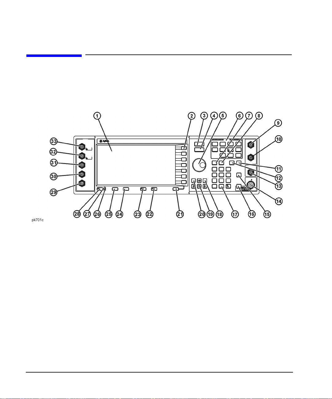
E4438C Vector Signal Generator Overview
Front Panel Overview
Front Panel Overview
Figure 2-1 shows the signal generator front panel. This interface enables you to define, monitor, and manage
input and output characteristics.
Figure 2-1 Front Panel Feature Overview
1. Display
The LCD screen provides information on the current function. Information can include status indicators,
frequency and amplitude settings, and error messages. Labels for the softkeys are located on the right-hand
side of the display. For further description of the front panel display, refer to “Front Panel Displ ay” on page
33.
2. Softkeys
Softkeys activate the function indicated by the displayed label to the left of each key.
3. Frequency Key
Pressing this hardkey makes frequency the active function. You can change the RF output frequency or use
the menus to configure frequency attributes such as frequency multiplier, offset, and reference.
26 Chapter 2
Page 51

E4438C Vector Signal Generator Overview
Front Panel Overview
4. Amplitude Key
Pressing this hardkey activates the amplitude function.
When active, the following functions also display indicators in the amp litude area:
•Amplitude offset (OFFS)
•Amplitude reference mode (REF)
•Alternate Amplitude (∆ = 0.00 dB)
•User flatness (UF)
5. Knob
Rotating the knob increases or decreases a numeric value or changes a highlighted digit or character. You
can also use the knob to step through lists or select items in a row. The knob uses the
conjunction with the knob ratio (set with the
the knob changes the active function value. For example, if the
and the knob ratio is 50 to 1, then each turn of the knob changes the active function by 0.2 dB (1/50th of
10 dB). By modifying either value or both, you change the amount for each turn of the knob. For more
information on softkeys, refer to the E4428C/38C ESG Signal Generators Key and Data Field Reference.
Step/Knob Ratio softkey) to determine how much each turn of
Incr Set value for the active function is 10 dB
Incr Set value in
6. Menu Keys
These hardkeys access softkey menus enabling configuration of list and step sweeps, utility functions, the
LF output, and various analog and digital modulation types. For detailed information on these keys, refer to
the E4428C/38C ESG Signal Generators Key and Data Field Reference.
7. Save Key
This hardkey accesses a menu of softkeys enabling you to save instrument settings to the signal generator’s
instrument state memory register. The instrument state register is a section of memory divided into 10
sequences numbered 0 through 9. Each sequence contains 100 registers numbered 00 through 99.
The
Save hardkey provides a quick alternative to reconfiguring the signal generator via the front panel. The
Recall hardkey recalls a saved instrument state.
Refer to “Saving an Instrument State” on page 71 for more information on the save operation.
8. Recall Key
This hardkey restores any instrument state that you previously saved in a instrument state memory
register .W hen you load t he wavefo rm fi le fr om NVWFM into w aveform m emory ( WFM1), and then use th e
Recall softkey to recall the signal generator settings associated with the file.
Chapter 2 27
Page 52

E4438C Vector Signal Generator Overview
Front Panel Overview
9. EXT 1 INPUT Connector
This BNC input connector accepts an input signal for use with AM, FM, ΦM, and pulse modulation, or as
the linear control for a burst envelope. The damage levels are 5 V
AM, FM, ΦM ±1Vp produces the in dic a te d d e via tion or depth. When using the A C c o up le d in p ut s e lec tio n w ith a
signal that has a peak input voltage that differs from 1 V
displays the HI/LO annunciator.
Pulse Modulation +1 V is on and 0 V is off
Burst Envelope Provides linear c ontrol: −1 V = 0% amplitude and 0 V = 100% amplitude
and 10 Vp.
rms
by more than 3%, the signal generator
p
On signal generators with Option 1EM, this input is relocated to an SMB connector on the rear panel.
10. EXT 2 INPUT Connector
This BNC input connector accepts an input signal for use with AM, FM, ΦM, and pulse modulation. The
damage leve ls are 5 V
AM, FM, ΦM ±1Vp produces the indicated deviation or depth. When using the AC coupled input selection with a
signal that has a peak input voltage that differs from 1 V
displays HI/LO annunciator.
Pulse Modulation +1 V is on and 0 V is off
and 10 Vp.
rms
by more than 3%, the signal generator
p
If you configure your sign al generat o r with Opt ion 1E M, thi s inp ut is rel o cated to an S MB con nect or on the
rear panel.
11. Help Key
Press this key to display a short description of any hardkey or softkey. There are two help modes available:
single and continuous. Single mode is the factory preset condition. To toggle between single and continuous
mode, press
Single Mode The help text is provided for the next key you press without activating the key’s function. Any key
Continuous Mode The help text is provided for each subsequent key press until you either press the
Utility > Instrument Info/Help Mode > Help Mode Single Cont.
pressed afterward exits the help mode and activates the key’s function
change to single mode. In contin uous mode, pressing t he
(except for the
Preset key).
Help key again, or
Help key also activates the key’s function
12. Trigger Key
This hardkey initiates an immediate trigger event for a function such as a list or step sweep. The trigger
mode must be set to
28 Chapter 2
Tri g g er K e y prior to initiating a trigger event with this hardkey.
Page 53

E4438C Vector Signal Generator Overview
Front Panel Overview
13. LF OUTPUT Connector
This BNC connector is the output for modulation signals generated by the low frequency (LF) source
function generator. This output is capable of driving 3 V
On signal generators with Option 1EM, this output relocated to a rear-panel SMB connector.
(nominal) into a 50Ω load.
p
14. RF OUTPUT Connector
This female Type-N connector is the output for RF signals. The source impedance is 50Ω. For Options 501,
502, 503, and 504 the damage levels are 50 Vdc, 50 W at ≤ 2 GHz, and 25 W at > 2 GHz maximum. For
Options 501, 502, 503, and 504 the reverse power protection circuit will trip, however, at nominally 1 W.
CAUTION E4428C and E4438C signal generators with Option 506 are not equipped with reverse
power protection circuits.
On signal generators with Option 1EM, this output relocated to a rear-panel female Type-N connector.
15. Mod On/Off Key
Pressing this hardkey enables or disables all active modulation formats (AM, FM, ΦM, Pulse, or I/Q) that
are applied to the output carrier signal.
This hardkey does not set up or activate an AM, FM, ΦM, Pulse, or I/Q format; each individual modulation
format must still be set up and activated (for example,
carrier signal when the
The MOD ON/OFF a nnu nciator, which is always present on the display, indicates whether active modulation
formats have been enabled or disabled with the
Mod On/Off hardkey is enabled.
AM > AM On) or nothing will be applied to the output
Mod On/Off hardkey.
16. RF On/Off Key
This hardkey toggles the operating state of the RF signal present at the RF OUTPUT connector. The
RF On/Off annunciator is always visible in the display to indicate whether the RF is turned on or off.
17. Numeric Keypad
The numeric keypad consists of the 0 th rough 9 hardke ys, a decimal p oint hard key, and a backspace hardkey
( ). The backspace hardkey enables you to backspace or specify a negative value. When specifying a
negative numeric valu e, the negative sign must be entered prior to entering the numeric value.
Chapter 2 29
Page 54

E4438C Vector Signal Generator Overview
Front Panel Overview
18. Incr Set Key
This hardkey enables you to set the increment value of the current active function. When this hardkey is
pressed, the increment value of the current active function appears as the active entry for the display . Use the
numeric keypad, arrow hardkeys, or the knob to adjust the increment value. Changing the Incr Set hardkey’s
value also affects how much each turn of the knob changes an active function’s value according to the
knob’s current ratio setting. For more information on softkeys, refer to the E4428C/38C ESG Signal
Generators Key and Data Field Reference.
19. Arrow Keys
The up and down arrow hardkeys are used to increase or decrease a numeric value, step through displayed
lists, or select items in a row of a disp l ayed l ist. Individual digits or characters may be highlighted using the
left and right arrow hardkeys. Once an individual digit or character is highlighted, its value can be changed
using the up and down arrow hardkeys.
20. Hold Key
This hardkey blanks the softkey label area, the active function area, and the text areas of the display.
Softkeys, arrow hardkeys, the knob, the numeric keypad, and the
hardkey is pressed. Press any other hardkey to end the hold mode.
Incr Set hardkey have no effect once this
21. Return Key
This hardkey enables you to retrace your key presses. When in a menu with more than one level (More 1 of
3, More 2 of 3, etc.), the
Return key will always return you to the first level of the menu.
22. Display Contrast Increase Key
This hardkey, when pressed or held, causes the display background to darken.
23. Display Contrast Decrease Key
This hardkey, when pressed or held, causes the display background to lighten.
24. Local Key
This hardkey is used to deactivate remote operation and return the signal generator to front panel control.
25. Preset Key
This hardkey is used to set the signal generator to a known state (factory or user-defined).
30 Chapter 2
Page 55

E4438C Vector Signal Generator Overview
Front Panel Overview
26. Standby LED
This yellow LED indicates when the signal generator power switch is set to the standby condition.
27. Line Power LED
This green LED indicates when the signal generator power switch is set to the on position.
28. Power Switch
This switch activates full power to the signal generator when set to the on position, and deactivates all signal
generator functions when in standby mode. In standby mode, the signal generator remains connected to the
line power, and power is supplied to some internal circuits.
29. SYMBOL SYNC Connector (Option 001/601 or 002/602)
This female BNC input connector accepts an externally supplied symbol sync signal for use with digital
modulation applications. The expected input is a CMOS bit clock signal. It may be used in two modes.
When used as a symbol sync in conjunction with a data clock, the signal must be high during the first data
bit of the symbol. The signal must be valid during the falling edge of the data clock signal and may be a
single pulse or continuous. When the SYMBOL SYNC itself is used as the (symbol) clock, the CMOS
falling edge is used to clock the DATA signal.
The maximum clock rate is 50 MHz. The d
On signal generators with Option 1EM, this input is relocated to a rear panel SMB connector.
When using the real-time W-CDMA uplink personality, this connector should not be used to connect the
external baseband generator data clock. The BASEBAND GEN REF IN connector should be used instead.
amage levels are > +5.5 volts and < −0.5 volts.
30. DATA CLOCK Connector (Option 001/601 or 002/602)
The female BNC input connector accepts a CMOS externally supplied CMOS compatible signal data-clock
input used with digital modulation applications. The expected input is a CMOS bit clock signal where the
rising edge is aligned with the beginning data bit. The falling edge is used to clock the DAT A and SYMBOL
SYNC signals.
The maximum clock rate is 50 MHz. The damage levels are > +5.5 volts and < −0.5 volts.
On signal generators with Option 1EM, this input is relocated to a rear panel SMB connector.
Chapter 2 31
Page 56

E4438C Vector Signal Generator Overview
Front Panel Overview
31. DATA Connector (Option 001/601 or 002/602)
The female BNC input connector accepts a CMOS externally supplied CMOS compatible signal data input
used with digital modulation applications. The expected input is a CMOS signal where a CMOS high is
equivalent to a data 1 and a CMOS low is equivalent to a data 0.
The maximum input data rate is 50 Mb/s.The data must be valid on the DATA CLOCK falling edges. The
damage levels are > +5.5 volts and < − 0.5 volts.
On signal generators with Option 1EM, this input is relocated to a rear panel SMB connector.
32. Q Connector
This female BNC input connector accepts an externally supplied, analog, quadrature-phase component of
I/Q modulation. The signal level is = 0.5 V
50Ω. The damage level is 1 V
and 10 volts peak.
rms
for a calibrated output level. The input impedance is
rms
To activate a signal applied to this connector, press
Ext 50 Ohm or Ext 600 Ohm. On signal generators with Option 1EM, this input is relocated as an SMB to the
Mux > I/Q Source 1 or I/Q Source 2 and then select either
rear panel.
33. I Connector
This female BNC input connector accepts an externally supplied, analog, in-ph ase componen t of I/Q
modulation. The signal level is = 0.5 V
To activate the in-phase component of the I/Q signal applied to this connector, press
I/Q Source 2 and then select either Ext 50 Ohm or Ext 600 Ohm.
This input connector also accepts the modulating signal for use with the wideband AM selection. The
wideband AM signal depth is a linear function of the I INPUT signal voltage:
• 0.25 volts = 50%
• 0.5 volts = 100%
When turned on, wideband AM automatically selects the I INPUT and configures it for 50Ω. This setting is
independent of the
The damage level for this connector is 1 V
MUX > I/Q Source setting.
rms
input is relocated as an SMB to the rear panel.
for a calibrated output level. The input impedance is 50Ω.
rms
Mux > I/Q Source 1 or
and 10 volts peak. On signal generators with Option 1EM, this
32 Chapter 2
Page 57

E4438C Vector Signal Generator Overview
Front Panel Display
Front Panel Display
Figure 2-2 shows the front panel display. The LCD screen displa ys data fi elds, annotat ions, key pr ess results ,
softkey labels, error messages, and annunciators that represent various active functions.
Figure 2-2 Front Panel Display
1. Frequency Area
The current frequency setting is shown in this portion of the display. In this same area, the ESG displays the
indicators for frequency offset (OFFS) and multiplier (MULT) functions. In addition, REF appears when you
enable the frequency reference mode and CHANNEL is turned on when you turn on a frequency channel
(
Freq Channels Off On softkey).
Chapter 2 33
Page 58

E4438C Vector Signal Generator Overview
Front Panel Display
2. Annunciators
The display annunciators show the status of some of the signal generator functions, and indicate error
conditions. An annunciator position may be used by more than one function. This does not create a problem,
because only one function that shares an annunciator position can be active at a given time.
ΦM This annunciator appears when phase modulati on i s t urn ed on . If frequency modulation
is turned on, the FM annunciator will replace ΦM.
ALC OFF This annunciator appears when the ALC circuit is disabled. Two other annunciators
appear in the same position: UNLEVEL when the ALC is enabled and is unable to
maintain the output level, and BBG DAC when the waveform data exceeds the DAC
range.
AM This annunciator appears when amplitude modulation is turned on.
ARMED This annunciator appears when a sweep has been initiated and the signal generator is
waiting for the sweep trigger event.
ATTEN HOLD This annunciator appears when the attenuator hold function is turned on. When this
function is on, the attenuator is held at its current setting.
BERT This annunciator appears when the Option UN7 bit error rate test (BERT) functions are
turned on.
ENVLP This annunciator appears if the burst envelope modulation is turned on.
ERR This annunciator appears when an error message is placed in the error queue. This
annunciator will not turn off until you have viewed all of the error messages or cleared
the error queue. You can access error messages by pressing
Utility > Error Info.
EXT1 LO/HI This annunciator is displayed as ei ther EXT1 LO or EXT1 HI. This annunciator appears
when the ac-coupled signal to the EXT 1 INPUT is less than 0.97 V
1.03 V
.
p
or greater than
p
EXT2 LO/HI This annunciator is displayed as ei ther EXT2 LO or EXT2 HI. This annunciator appears
when the ac-coupled signal to the EXT 2 INPUT is less than 0.97 V
1.03 V
.
p
or greater than
p
EXT REF This annunciator appears when an external frequency reference is applied.
FM This annunciator appears when frequency modulation is turned on. If ph ase modu lation
is turned on, the ΦM annunciator will replace FM.
L This annunciator appears when the signal generator is in listener mode and is receiving
information or commands over the GPIB, RS-232, or VXI-11/Sockets (LAN) interface.
34 Chapter 2
Page 59

E4438C Vector Signal Generator Overview
Front Panel Display
MOD ON/OFF This annunciator indicates if the RF carrier is modulated (MOD ON while there is an
active modulation format), or if the modulation is off (MOD OFF). Either condition of
this annunciator is always visible in the display.
The MOD ON annunciator may be showing even when there are no active modulation
formats. This merely indicates that the carrier signal will be modulated when a
modulation format is enabled.
OVEN COLD This annunciator appears when the temperature of the internal oven reference oscillator
has dropped below an acceptable level. When this annunciator is on, frequency
accuracy is degraded. This condition should occur for several minutes after the signal
generator is first connected to line power. The annunciator is timed, and automatically
turns off after a specified period.
PULSE This annunciator appears when pulse modulation is turned on.
R This annunciator appears when the signal generator is remotely controlled over the
GPIB, RS-232, or VXI-11/Sockets (LAN) interface.
RF ON/OFF This annunciator indicates when the RF signal is present (RF ON) at the RF OUTPUT,
or if the RF signal is not present (RF OFF) at the RF OUTPUT. Either condition of this
annunciator is always visible in the display.
S This annunciator appears when the signal generator has generated a service request
(SRQ) over the GPIB, RS-232, or VXI-11/Sockets (LAN) interface.
SWEEP This annunciator appears when the signal generator is sweeping in list or step mode.
T This annunciator appears when the signal generator is in talker mode and is transmitting
information over the GPIB, RS-232, or VXI-11/Sockets (LAN) interface.
UNLEVEL This annunciator appears when the signal generator is unable to maintain the correct
output level. The UNLEVEL annunciator is not necessarily an indication of instrument
failure. Unleveled conditions can occur during normal operation. Two other
annunciators appear in the same position: ALC OFF when the ALC circuit is disabled
and BBG DAC when the waveform data exceeds the DAC range.
BBG DAC This annunciator appears when the waveform data exceeds the range of th e DAC, which
causes a DAC over-range error. It remains illuminated until the condition is corrected by
scaling the data. It appears in the same location as the UNLEVEL and ALC OFF
annunciators, and is the dominant annunciator. For example, if an unleveled condition
exists at the same time as a DAC over -range condition, the DAC over -range annunciato r
remains until corrected. Once corrected, the UNLEVEL annunciator appears.
UNLOCK This annunciator appears when any of the phase locked loops are unable to maintain
phase lock. You can determine which loop is unlocked by examining the error
messages.
Chapter 2 35
Page 60

E4438C Vector Signal Generator Overview
Front Panel Display
3. Digital Modulation Annunciators
All digital modulation annunciators appear in this location. These annunciators appear only wh en the
modulation is active, and only one digital modulation can be active at any given time.
4. Amplitude Area
The current output power level setting is shown in this portion of the display. When active, the following
functions also display indicators in the amplitude area:
• Amplitude offset (OFFS)
• Amplitude reference mode (REF)
• Alternate Amplitude (∆ = 0.00 dB)
• User flatness (UF)
5. Softkey Label Area
The labels in this area define the function of the softkeys located immediately to the right of the label. The
softkey label will change depending upon the function selected. For detailed softkey descriptions, refer to
the E4428C/38C ESG Signal Generators Key and Data Field Reference.
6. Error Message Area
Abbreviated error messages are reported in this space. When multiple error messages occur, only the most
recent message remains displayed. Reported error messages with details can be viewed by pressing
Error Info.
Utility >
7. Text Area
This area of the display is used to show status information about the signal generator such as the modulation
status, sweep lists, and file catalogs. This area also enables you to perform functions such as managing
information, entering information, and displaying or deleting files.
8. Active Function Area
The current active function is shown in this area. For example, if frequency is the active function, the current
frequency setting will be displayed here. If the current active function has an increment value associated
with it, that value is also displayed.
36 Chapter 2
Page 61

E4438C Vector Signal Generator Overview
Rear Panel Overview
Rear Panel Overview
The signal generator rear panel (Figure 2-3) provides input, output, and remote interface connections.
Figure 2-4 shows a portion of the rear panel for signal generators with Option 1EM, which moves front
panel connectors to the rear panel. For Option 1EM connectors not described in this section, see
“Front Panel Overview” on page 26.
Figure 2-3 Rear Panel Feature Overview
Figure 2-4
Chapter 2 37
Page 62

E4438C Vector Signal Generator Overview
Rear Panel Overview
1. 321.4 IN Connector (Option 300)
Use this female SMB connector to input a downconverted 321.4 MHz GSM/EDGE signal for base
transceiver station (BTS) loopback measurements. (Option 300 also requires Options UN7, 001/601or
002/602, and 402).
2. BER GATE IN Connector (Option UN7)
Use this female SMB connector to input the clock gate signal for the bit-error-rate measurements. The clock
signal to the BER CLK IN connector is valid only when the signal to this connector is a high or low,
depending on your softkey selection or SCPI command. The d
This connector accepts a high impedance TTL-compatible signal or a 75Ω input. It can be enabled or
disabled by a softkey or a SCPI command.
amage levels are > +5.5 volts and < −0.5 volts.
3. BER CLK IN Connector (Option UN7)
Use this female SMB connector to input the clock signal for the bit-error-rate measurements. The rising
(positive) or falling (negative) edge of the signal (selected either by softkey or SCPI command) causes data
on the BER DATA IN connector to be sampled. The d
connector accepts a high impedance TTL-compatible signal or a 75Ω input.
amage levels are > +5.5 volts and < −0.5 volts. This
4. BER DATA IN Connector (Option UN7)
Use this female SMB connector to input the data streams for the bit-error-rate measurements. The rising
(positive) or falling (negative) edge of the BER CLK IN signal (selected by the softkey or the SCPI
command) is used to trigger the reading of the data. The d
connector accepts a high impedance TTL-compatible signal or a 75Ω input.
amage lev els are > +5.5 volts and < −0.5 volts. This
5. I-bar OUT Connector (Option 001/601 or 002/602)
This female BNC connector is used in conjunction with the I OUT connector to provide a balanced baseband
stimulus. Balanced signals are signals present in two separate conductors that are symmetrical relative to
ground, and are opposite in polarity (180 degrees out of phase). The nominal output impedance of this
connector is 50Ω, DC-coupled. The damage levels are > +2 V and < −2 V. The DC origin offset is typically
< 10 mV. The output signal levels into a 50Ω load are as follows:
• 0.5 V
• 0.69 V
• 0.71 Vpk (3.08 dB), typical, maximum crest factor for peaks for π/4 DQPSK with alpha = 0.35.
• Typically 1 V
38 Chapter 2
, typical, corresponds to one unit length of the I/Q vector.
pk
(2.84 dB), typical, maximum crest factor for peaks for π/4 DQPSK with alpha = 0.5.
pk
maximum (Option 001/601or 002/602 only).
p-p
Page 63

E4438C Vector Signal Generator Overview
Rear Panel Overview
If you configure your si gnal generato r with Option 1EM, this outp ut is relocated an d changed fro m a BNC to
an SMB connector.
6. I OUT Connector (Option 001/601 or 002/602)
This female BNC connector outputs the analog, in-phase component of I/Q modulation from the internal
baseband generator. The nominal output impedance of this connector is 50Ω, DC-coupled. The damage
levels are > +3.5 V and < −3.5 V. The DC origin offset is typically < 10 mV. The output signal levels into a
50Ω load are as follows:
• 0.5 V
• 0.69 V
• 0.71 V
• Typically 1 V
, typical, corresponds to one unit length of the I/Q vector.
pk
(2.84 dB), typical, maximum crest factor for peaks for π/4 DQPSK with alpha = 0.5.
pk
(3.08 dB), typical, maximum crest factor for peaks for π/4 DQPSK with alpha = 0.35.
pk
maximum.
p-p
If you configure your signal generator with Option 1EM, this output is relocated from a BNC to an SMB
connector.
7. COH CARRIER Output Connector
The coherent carrier connector outputs R F that is modulated with FM or ΦM. The output power is nominally
–2 dBm ±5 dB. The output frequency range is from 249.99900001 MHz to the maximum specified
frequency of your signal generator or 4 GHz for Option 506 instruments. If the RF output frequency is
below this range, the coherent carrier output signal will have the following frequency: Frequency of
coherent carrier = (1E9 − Frequency of RF output) in Hz. The d amage levels are 20 Vdc and 13 dBm reverse
RF power.
8. Q OUT Connector (Option 001/601 or 002/602)
This female BNC connector outputs the analog, quadrature-phase component of I/Q modulation from the
internal baseband generator. The nominal output impedance of this connector is 50Ω, DC-coupled. The
damage levels are > +3.5 V and < −3.5 V. The DC origin offset is typically < 10 mV. The output signal
levels into a 50Ω load are as follows:
• 0.5 V
• 0.69 V
• 0.71 V
• Typically 1 V
, typical, corresponds to one unit length of the I/Q vector.
pk
(2.84 dB), typical, maximum crest factor for peaks for π/4 DQPSK with alpha = 0.5.
pk
(3.08 dB), typical, maximum crest factor for peaks for π/4 DQPSK with alpha = 0.35.
pk
maximum.
p-p
If you configure your signal generator with Option 1EM, this output is relocated from a BNC to an SMB
connector.
Chapter 2 39
Page 64

E4438C Vector Signal Generator Overview
Rear Panel Overview
9. Q-bar OUT Connector (Option 001/601 or 002/602)
This female BNC connector is used in conjunction with the Q OUT connector to provide a balanced
baseband stimulus. Balanced signals are signals present in two separate conductors that are symmetrical
relative to ground, an d are op posi te in pola rity (180 degrees out o f phas e). The n ominal output i mpedan ce of
this connector is 50Ω, DC-coupled. The damage levels are > +2 V and < −2 V. The DC origin offset is
typically < 10 mV. The output signal levels into a 50Ω load are as follows:
• 0.5 V
• 0.69 V
• 0.71 V
• Typically 1 V
, typical, corresponds to one unit length of the I/Q vector.
pk
(2.84 dB), typical, maximum crest factor for peaks for π/4 DQPSK with alpha = 0.5.
pk
(3.08 dB), typical, maximum crest factor for peaks for π/4 DQPSK with alpha = 0.35.
pk
maximum.
p-p
If you configure your signal generator with Option 1EM, this output is relocated from a BNC to an SMB
connector.
10. EVENT 1 Connector (Option 001/601 or 002/602)
This female BNC connector outputs a pulse that can be used to trigger the start of a data pattern, frame, or
timeslot. It is adjustable to within plus or minus one timeslot with one bit of resolutio n. With Option 401
installed, an even second output is generated. A marker is output every t wo seconds ind icating the beginn ing
of each short code sequence for use in synchronizing CDMA analysis instruments.
There is a marker on/off condition associated with each waveform point. The marker 1 level is +3.3 V
CMOS high when positive polarity is selected; –3.3 V CMOS low when negative polarity is selected. The
output on the EVENT 1 connector occurs whenever Marker 1 is turned on in the waveform. (Markers are
automatically turned on whenever you set them in a waveform segment. When you combine waveform
segments that contain Marker 1 into a sequence, the markers are automatically turned off until you toggle
them on in either the Edit Selected Waveform Sequence menu or in the Build New Waveform Sequence
menu.)
The damage levels for the Event 1 connector are > +8 V and < −4 V. On signal generators wi th Option 1EM,
this output is changed from a BNC to an SMB connector. With Option 401 you can select from several
different output signals for this connector.
11. EVENT 2 Connector (Option 001/601 or 002/602)
This female BNC connector outputs a data enable signal for gating external equipment. The output is
applicable when the external data is clocked into internally generated timeslots. Data is enabled when the
signal is low. With Option 401 installed, a marker is output on the EVENT 2 connector every
26.67 milliseconds, corresponding to the start of each short code.
There is a marker on/off condition associated with each waveform point. The marker 2 level is +3.3 V
CMOS high when positive polarity is selected; –3.3 V CMOS low when negative polarity is selected. The
40 Chapter 2
Page 65

E4438C Vector Signal Generator Overview
Rear Panel Overview
output on the EVENT 1 connector occurs whenever Marker 1 is turned on in the waveform.The output on
the EVENT 2 connector occurs whenever Marker 2 is turned on in the waveform. (Markers are
automatically turned on whenever you set them in a waveform segment. When you combine waveform
segments that contain Marker 2 into a sequence, the markers are automatically turned off until you toggle
them on in either the Edit Selected Waveform Sequence menu or in the Build New Waveform Sequence
menu.)
The damage levels are > +8 V and < −4 V. On signal generators with Option 1EM, this output is changed
from a BNC to an SMB connector. With Option 401 this connector is used for system reset output.
12. PATT TRIG IN Connector (Option 001/601 or 002/602)
This female BNC input connector can accept either a CMOS low to CMOS high, or CMOS high to CMOS
low edge trigger. The minimum trigger input pulse width, high or low, is 100 ns. The damage levels are
> +5.5 volts and < −0.5 volts. If you configure your signal generator with Option 1EM, this input is
changed from a BNC to an SMB connector.
The input to the P ATT TRIG IN connector is used to trigger the internal digital modulation pattern generator
to start a single pattern output or to stop and re-synchronize a pattern that is being continuously output. The
trigger edge is latched and then sampled by the falling edge of the internal data bit clock to synch r onize the
trigger with the data bit clock timing. The minimum delay from the trigger edge to the first bit of the frame
is 1.5 to 2.5 bit clock periods.
This connector is the source for the external trigger for all of the ARB waveform generator triggers. With
Option 401, this connector is used for even second synchronization input.
13. AUX I/O Connector
This female 37-pin connector is active only on instruments with an internal baseband generator (Option
001/601or 002/602); on signal generators without one of these options, this connector is non-functional.
This connector provides access to the inputs and outputs described in the following table and shown in
Figure 2-5.
Connector Pin
ALT PWR IN Pin-16 of the Aux I/O connector is used with an internal baseband generator. This pin
accepts a CMOS signal for synchronization of external data and alternate power signal
timing. Damage levels are > +5.5 volts and < −0.5 volts.
DATA CLK OUT Pin-6 of the Aux I/O connector is used with an inter nal baseband generato r. This pin
relays a CMOS bit clock signal for synchronizing serial data. Damage levels are >
+5.5 volts and < −0.5 volts.
DATA OUT Pin-7 of the Aux I/O connector is used with an inter nal baseband generator. This pin
outputs data (CMOS) fro m t he inte rnal d ata ge nerator or t he ex ternally supplie d sign al at
data input. Damage levels are > +5.5 volts and < −0.5 volts.
Description
Chapter 2 41
Page 66

E4438C Vector Signal Generator Overview
Rear Panel Overview
Connector Pin
EVENT 3 Pin-19 of the Aux I/O connecto r is used wit h an internal ba seband ge nerato r. In arbitrary
waveform mode, this pin outputs a t iming signal generated by Marker 3.
The marker 3 output level is +3.3 V CMOS regardless of marker polarity settings.The
reverse damage levels for this connect or pin are > +5.5 volts and < −0.5 volts.
EVENT 4 Pin-18 of the Aux I/O connecto r is used wit h an internal ba seband ge nerato r. In arbitrary
waveform mode, this pin outputs a t iming signal generated by Marker 4.
The marker 4 output level is +3.3 V CMOS regardless of marker polarity settings. The
reverse damage levels for this connect or pin are > +5.5 volts and < −0.5 volts.
P ATT TRIG IN 2 Pin-17 of the Aux I/O connector accepts a signal that triggers an internal p attern or fra me
generator to start single patte rn output. Minimum pulse width is 100 ns. Damage levels
are > +5.5 and < −0.5 V.
SYM SYNC OUT Pin-5 of the Aux I/O connector is used with an internal baseband generator. This pin
outputs the CMOS symbol cl ock for symbol synchronization, one data clock period
wide. Damage levels are > +5.5 volts and < −0.5 volts.
BER MEAS TRIG/BER
NO DATA
BER ERR OUT Pin-21 is used for bit error rate testing (Option UN7). Damage levels are > +5.5 volts
BER TEST OUT Pin-20 is used for bit error rate testing (Option UN7). Damage levels are > +5.5 volts
Pin-22 is used for bit error rate testing (Option UN7). Damage levels are > +5.5 volts
and < −0.5 volts.
and < −0.5 volts
and < −0.5 volts
Description
(Continued)
BER SYNC LOSS Pin-4 is used for bit error rate testing (Option UN7). Damage le vels a re > + 5. 5volts and
< −0.5 volts.
BER MEAS END Pin-1 is used for bit error rate testing (Option UN7). Damage le vels a re > +5. 5volts and
< −0.5 volts.
42 Chapter 2
Page 67

Figure 2-5 AUX I/O Pin Configuration
E4438C Vector Signal Generator Overview
Rear Panel Overview
View looking into
rear panel connec to r
14. DIGITAL BUS
This is a proprietary bus used for Agilent Bas eban d Studio products, which require Option 601 or 602 . Thi s
connector is not operational for general purpose customer use. Signals are present only when a Baseband
Studio option is installed (for details, refer to www.agilent.com/find/basebandstudio).
15. AC Power Receptacle
The power cord receptacle accepts a three-pronged cable that is shipped with the signal generator. The line
voltage is connected here.
Chapter 2 43
Page 68

E4438C Vector Signal Generator Overview
Rear Panel Overview
16. GPIB Connector
The GPIB connector allows communications with compatible devices such as external controllers. It is
functionally equivalent to the LAN and RS 232 connectors.
17. RS 232 Connector
This female DB-9 connector is an RS-232 serial port that can be used for controlling the signal generator
remotely. It is functionally equivalent to the GPIB and LAN connectors. The following table shows the
descripti on of the pinouts. Figure 2-6 shows the pin configuration.
Table 2-1 RS 232 Connector
Pin Number Signal Description Signal Name
1 No Connection
2 Receive Data RECV
3 Transmit Data XMIT
4+5 V
5 Ground, 0 V
6 No Connection
7Request to SendRTS
8 Clear to Send CTS
9 No Connection
Figure 2-6
View looking into
rear panel conn ector
18. LAN Connector
LAN based communication is supporte d by the signal gen erator via the LAN (local a rea network) connector.
The LAN connector enables the signal generator to be remotely programmed by a LAN-connected
computer . The distance between a computer and the sign al gen erat or is l imi te d to 100 meters (10Base-T) on
a single cable. For more information about the LAN, refer to the E4428C/38C ESG Signal Generators
Programming Guide.
44 Chapter 2
Page 69

E4438C Vector Signal Generator Overview
Rear Panel Overview
19. TRIG OUT Connector
This female BNC connector outputs a TTL signal that is asserted high at the start of a dwell sequence, or at
the start of waiting for the point trigger in manual sweep mode. It is asserted low when the dwell is over,
when the point trigger is received, or once per sweep during an LF sweep. The logic polarity can be
reversed.
20. BURST GATE IN Connector (Option 001/601 or 002/602)
The female BNC connector accepts a CMOS signal for gating burst power in digital modulation
applications. The burst gating is used when you are externally supplying data and clock information. The
input signal must be synch ronized with t he extern al data input that will be ou tput dur ing the bur st. The bu rst
power envelope and modulated data are internally delayed and re-synchronized. The input signal must be
CMOS high for normal burst RF power or CW RF output power and CMOS low for RF off. The leading
edges must be synchronous with the DATA CLOCK rising edges. The damage levels are > +5.5 volts and
< −0.5 volts.
If you configure your signal generator with Option 1EM, this output is changed from a BNC to an SMB
connector. With Option 401, this connector is u sed for system res e t tr igger input.
21. TRIG IN Connector
This female BNC connector accepts a CMOS signal for triggering operations, such as point-to-point in
manual sweep mode or an LF sweep in external sweep mode. Triggering can occur on either the positive or
negative edge. The d
amage levels are > +5.5 volts and < −0.5 volts.
22. 10 MHz IN Connector
This female BNC connector accepts a −3.5 to +20 dBm signal from an external timebase reference that is
within ±10 ppm (standard timebase) or ±1 ppm (high stability timebase). The nominal input impedance is
50Ω. The signal generator detects when a valid reference signal is present at this connector and
automatically switches from internal to external reference operation. The signal generator will o nl y
automatically switch from internal to external reference operation when the instrument is in its factory
default mode where the
Ref Oscillator Source Auto Off On softkey is set to on.
23. SWEEP OUT Connector
This female BNC connector provides a voltage range of 0 to +10 V. When the signal generator is sweeping,
the SWEEP OUT signal ranges from 0 V at the beginning of the sweep to +10 V at the end of the sweep
regardless of the sweep width . In CW mo de t his conn ect or h as n o ou t put. The output impedance is less than
1Ω and can drive 2 kΩ.
Chapter 2 45
Page 70

E4438C Vector Signal Generator Overview
Rear Panel Overview
24. 10 MHz OUT Connector
This female BNC connector provides a nominal signal level of +3.9 dBm ±2 dB, and an output impedance
of 50Ω. The accuracy is determined by the timebase used.
25. BASEBAND GEN REF IN Connector (Option 001/601 or 002/602)
The BASEBAND GEN REF IN connector accepts a 0 to +20 dBm sine wave or TTL square wave signal
from an external timebase reference. This digital modulation reference clock is used by the internal
baseband generator for both component and receiver test applications (only the internal baseband generator
can be locked to this external reference; the RF frequency remains locked to the 10 MHz reference). The
nominal input impedance is 50Ω at 13 MHz, AC-coupled.
This connector accepts a TTL or > −10 dBm sine wave external reference at rates from 250 kHz through
100 MHz. The internal clock for the arbitrary waveform generator is locked to this signal when external
reference is selected in the ARB setup. The minimum pulse width must be > 10 ns. The damage levels are
> +8 V and < −8 V.
This female BNC connector is provided only on signal generators with Options 001/601 and 002/602. On
signal generators with Option 1EM, this output is changed from a BNC to an SMB connector.
When using the real-time W-CDMA uplink personality, this connector is used to connect the external
baseband generator data clock.
46 Chapter 2
Page 71

3 Basic Operation
The following list shows the topics covered in this chapter:
• “Using Table Editors” on page 48
• “Configuring the RF Output” on page 50
• “Generating the Modulation Format” on page 58
• “Modulating the Carrie r Signal” on p age 60
• “Creating and Applying User Flatness Correction” on page 61
• “Using the Memory Catalog” on page 68
• “Using the Instrument State Registers” on page 70
• “Using Security Functions” on page 75
• “Enabling Options (E4438C Only)” on page 83
• “Using the Web Server” on page 85
47
Page 72

Basic Operation
Using Table Editors
Using Table Editors
The signal generator table editors enable you to simplify configuratio n tasks , such as creatin g a lis t sweep .
This section familiarizes you with basic table editor functionality using the List Mode V alues table editor as
an example.
Press
Preset > Sweep/List > Configure List Sweep.
The signal generator displays the List Mode Values table editor, as shown below.
Figure 3-1
Active Function Area
Ta ble Editor Name
Tabl e Items
Cursor
Table Editor Softkeys
Active Function Area displays the acti ve table item while its value is edited.
Cursor an inverse video identifier used to highlight specific table items for
selection and editing.
Table Editor Softkeys select table items, preset table values, and modify table structures.
T able Items values arranged in numbered rows and titled columns (The columns
are also known as data fields. For example, the column below the
Frequency title is known as the Frequency data field).
48 Chapter 3
Page 73

Basic Operation
Using Table Editors
Table Editor Softkeys
The following table editor softkeys are used to load, navigate, modify, and store table item values. Press
More (1 of 2) to access Load/Store and its associated softkeys.
Edit Item displays the selected item in the active function area of the display where the item’s
value can be modified.
Insert Row inserts an identical row of table items above the currently selected row.
Delete Row deletes the currently selected row.
Goto Row opens a menu of softkeys (Enter, Goto Top Row, Goto Middle Row, Goto Bottom Row, Page Up,
and
Page Down) used to quickly navigate through the table items.
Insert Item inserts an identical item in a new row below the currently selected item.
Delete Item deletes the item from the bottom row of the currently selected column.
Page Up and
Page Down displays table items that occupy rows outside the limits of the ten-row table display
area.
Load/Store opens a menu of softkeys (Load From Selected File, Store To File, Delete File, Goto Row, Page
Up
, and Page Down) used to load table items from a file in the memory catalog, or to
store the current table items as a file in the memory catalog. The signal generator
accepts a file name with a maximum length of 23 characters (alphanumeric and special
characters).
Modifying Table Items in the Data Fields
To modify existing table items:
1. Use the arrow keys or the k nob to m ove the table cu rs or o ver the d esired item. In Fi gure 3-1 on page 48,
the first item in the Frequency data field has been selected.
2. Press
3. Use the knob, arrow keys, or the numeric keypad to modify the value.
4. Press
Chapter 3 49
Edit Item.
The selected item is displayed in the active function area of the display.
Enter.
The modified item is now displayed in the table.
Page 74

Basic Operation
Configuring the RF Output
Configuring the RF Output
This section will show you how to create continuous wave and swept RF outputs.
Configuring a Continuous Wave RF Output
Using these procedures, you will learn how to set the following parameters:
• RF output frequency
• frequency reference and frequency offset
• RF output amplitude
• amplitude reference and amplitude of fs et
Setting the RF Output Frequency
1. Press
NOTE You can change the preset condition of the signal generator to a user-defined state. For these
2. Observe the FREQUENCY area of the display (in the upper left-hand corner).
3. Press
4. Press
5. Press
Preset.
This returns the signal generator to the factory-defined state.
examples, however, use the factory-defined preset state (the
the Utility menu must be set to Normal).
The value displayed is the maximum specified frequency of the signal generator.
RF On/Off.
The
RF On/Off hardkey must be pressed before the RF signal is available at the RF OUTPUT connector.
The display annunciator changes from RF OFF to RF ON. The maximum specified frequency is now
being output at the RF OUTPUT connector (at the signal generator’s minimum power level).
Frequency > 700 > MHz.
The 700 MHz RF frequency is now displayed in the FREQUENCY area of the display and also in the
active entry area.
Frequency > Incr Set > 1 > MHz.
This changes the frequency increment value to 1 MHz.
Preset Normal User softkey in
50 Chapter 3
Page 75

6. Press the up arrow key.
Basic Operation
Configuring the RF Output
Each press of the up arrow key increases the frequency by the increment value last set with the
Incr Set
hardkey. The increment value is displayed in the active entry area.
7. The down arrow decreases the frequency by the increment value set in the previous step. Practice
stepping the frequency up and down in 1 MHz increments.
You can also adjust the RF output frequency using the knob. As long as frequency is the active function
(the frequency is displayed in the active entry area), the knob will increase and decrease the RF output
frequency.
8. Use the knob to adjust the frequency back to 700 MHz.
Setting the Frequency Reference and Frequency Offset
The following procedure set s the RF o utput freq uency as a reference frequency to which all other frequency
parameters are relative. The frequency initially shown on the display will be 0.00 Hz (the frequency output
by the hardware minus the reference frequency). Although the display changes, the frequency output does
not change. Any subsequent frequency changes are shown as incremental or decremental to 0 Hz.
1. Press
2. Press
3. Press
Preset.
Frequency > 700 > MHz.
Freq Ref Set.
This activates the frequency reference mode and sets the current output frequency (700 MHz) as the
reference value. The FREQUENCY area displays 0.00 Hz, which is the frequency output by the
hardware (700 MHz) minus the reference value (700 MHz). The REF indicator is activated and the
Freq Ref Off On softkey has toggled to On.
4. Press
RF On/Off.
The display annunciator has changed from RF OFF to RF ON. The RF frequency at the RF OUTPUT
connector is 700 MHz.
5. Press
Frequency > Incr Set > 1 > MHz.
This changes the frequency increment value to 1 MHz.
6. Press the up arrow key.
This increments the output frequency by 1 MHz. The FREQUENCY area display changes to show
1.000 000 00 MHz, which is the frequency output by the hardware (700 MHz + 1 MHz) minus the
reference frequency (700 MHz). The frequency at the RF OUTPUT changes to 701 MHz.
Chapter 3 51
Page 76

Basic Operation
Configuring the RF Output
7. Press Freq Offset > 1 > MHz.
This enters a 1 MHz offset. The FREQUENCY area displays 2.000 000 00 MHz, which is the
frequency output by the hardware (701 MHz) minus the reference frequency (700 MHz) plus the offset
(1 MHz). The OFFS indicator is activated. The frequency at the RF OUTPUT connector is still
701 MHz.
Setting the RF Output Amplitude
1. Press
Preset.
2. Observe the AMPLITUDE area of the display.
The display reads the minimum power level of the signal generator. This is the normal preset RF output
amplitude.
3. Press
RF On/Off.
The display annunciator changes from RF OFF to RF ON. The RF signal is now being output at the
minimum power level at the RF OUTPUT connector.
4. Press
Amplitude > –20 > dBm.
This changes the amplitude to −20 dBm. The new −20 dBm RF output power is now displayed in the
AMPLITUDE area of the display and also in the active entry area.
Amplitude is still the active function until you press another front pane l f unction key. You can also
change the amplitude using the up and down arrow keys and the knob.
Setting the Amplitude Reference and Amplitude Offset
The following procedure sets the RF output power as an amplitude reference to which all other am plit ude
parameters are relative. The amplitude initially shown on the display will be 0 dB (the power output by the
hardware minus the reference power ). Although the dis play changes, t he output powe r does not chang e. Any
subsequent power changes are shown as incremental or decremental to 0 dB.
1. Press
Preset.
2. Press
3. Press
Amplitude > –20 > dBm.
More (1 of 2) > Ampl Ref Set.
This activates the amplitude reference mode and sets the current output power (−20 dBm) as the
reference value. The AMPLITUDE area displays 0.00 dB, which is the power output by the hardware
(20 dBm) minus the reference value (−20 dBm). The REF indicator is activated and the
Ampl Ref Off On
softkey has toggled to On.
52 Chapter 3
Page 77

Basic Operation
Configuring the RF Output
4. Press RF On/Off.
The display annunciator has changed from RF OFF to RF ON. The power at the RF OUTPUT connector
is −20 dBm.
5. Press
Incr Set > 10 > dB.
This changes the amplitude increment value to 10 dB.
6. Use the up arrow key to increase the output power by 10 dB.
The AMPLITUDE area displays 10.00 dB, which is the power output by the hardware (-20 dBm plus
10 dBm) minus the reference power (−20 dBm). The power at the RF OUTPUT connector changes to
−10 dBm.
7. Press
Ampl Offset > 10 > dB.
This enters a 10 dB offset. The AMPLITUDE area displays 20.00 dB, which is the power output by the
hardware (−10 dBm) minus the reference power (−20 dBm) plus the offset (10 dB). The OFFS indicator
is activated. The power at the RF OUTPUT connector is still −10 dBm.
Configuring a Swept RF Output
The signal generator has two sweep types: step and list.
NOTE List sweep data cannot be saved within an instrument state, but can be saved to the memory
catalog. For instructions on saving list sweep data, see “Storing Files” on page 69.
During swept RF output, the FREQUENCY and AMPLITUDE areas of the signal generator’s
display are deactivated, depending on what is being swept.
This section provides an explanation of the differences between step sweep and list sweep. You will learn
two ways to configure the signal generator’s RF output to sweep a defined set of frequency and amplitude
points. You will create a step sweep and then you will use these points as the basis for a new list sweep.
Step Sweep
When a step sweep is activated, the signal generator sweeps the RF output based on the values entered for
RF output start and stop frequencies and amplitudes, a number of equally spaced points (steps) to dwell
upon, and the amount of dwell time at each point. The frequency, amplitude, or frequency and amplitude of
the RF output will sweep from the start amplitude/frequency to the stop amplitude/frequency, dwelling at
equally spaced intervals defined by the
# Points softkey value.
Step sweep provides a linear progression through the start-to-stop frequency and/or amplitude values. You
can toggle the direction of the sweep, up or down. When the
Sweep Direction Down Up softkey is set to Up,
Chapter 3 53
Page 78

Basic Operation
Configuring the RF Output
values are swept from the start frequency/amplitude to the stop frequency/amplitude. When set to Down,
values are swept from the stop frequency/amplitude to the start frequency/amplitude.
Configuring and Activating a Single Step Sweep
In this procedure, you will create a step sweep with nine, equally spaced points and the following
parameters:
• frequency range from 500 MHz to 600 MHz
• amplitude from −20 dBm to 0 dBm
• dwell time 500 ms at each point
1. Press
2. Press
Preset.
Sweep/List.
This opens a menu of sweep softkeys.
3. Press
Sweep Repeat Single Cont.
This toggles the sweep repeat from continuous to single.
4. Press
Configure Step Sweep.
5. Press Freq Start > 500 > MHz.
This changes the start frequency of the step sweep to 500 MHz.
6. Press
Freq Stop > 600 > MHz.
This changes the stop frequency of the step sweep to 600 MHz.
7. Press
Ampl Start > -20 > dBm.
This changes the amplitude level for the start of the step sweep.
8. Press
Ampl Stop > 0 > dBm.
This changes the amplitude level for the end of the step sweep.
9. Press
# Points > 9 > Enter.
This sets the number of sweep points to nine.
10. Press
Step Dwell > 500 > msec.
This sets the dwell time at each point to 500 milliseconds.
54 Chapter 3
Page 79

Basic Operation
Configuring the RF Output
11. Press Return > Sweep > Freq & Ampl.
This sets the step sweep to sweep both frequency and amplitude data. Selecting this softkey returns you
to the previous menu and turns on the sweep function.
12. Press
RF On/Off.
The display annunciator changes from RF OFF to RF ON.
13. Press
Single Sweep.
A single sweep of the frequencies and amplitudes configured in the step sweep is executed and available
at the RF OUTPUT connector. On the display, the SWEEP annunciator appears for the duration of the
sweep, and a progress bar shows the progr ession of the sweep. Th e
Single Sweep softkey can also be used
to abort a sweep in progress.
Activating Continuous Step Sweep
Press
Sweep Repeat Single Cont.
This toggles the sweep from single to continuous. A continuous repetition of the frequencies and amplitudes
configured in the step sweep are now available at the RF OUTPUT connector. The SWEEP annunciator
appears on the display, indicating that the signal generator is sweeping, and progression of the sweep is
shown by a progress bar.
List Sweep
List sweep allows you to create a list of arbitrary frequency, amplitude, and dwell time values and sweep the
RF output based on the entries in the List Mode Values table.
Unlike a step sweep that contains linear ascending/descending frequ ency and amplitude values spaced at
equal intervals throughout the sweep, list sweep frequencies and amplitudes can be entered at unequal
intervals, nonlinear ascending/descending, or random order.
For convenience, the List Mode Values table can be copied from a previously configured step sweep. Each
step sweep point’s associated frequency, amplitude and dwell time values are entered into a row in the List
Mode Values table, as the following example illustrates.
Configuring a List Sweep Using Step Sweep Data
In this procedure, you will leverage the step sweep points and change the sweep information by editing
several points in the List Mode Values table editor. For information on using table editors, see “Using Table
Editors” on page 48.
1. Press
Sweep Repeat Single Cont.
This toggles the sweep repeat from continuous to single. The SWEEP annunciator is turned off. The
sweep will not occur until it is triggered.
Chapter 3 55
Page 80

Basic Operation
Configuring the RF Output
2. Press Sweep Type List Step.
This toggles the sweep type from step to list.
3. Press
Configure List Sweep.
This opens another menu displaying softkeys that you will use to create the sweep points. The display
shows the current list data. (When no list has been previously created, the default list contains one point
set to the signal generator’s maximum frequency, minimum amplitude, and a dwell time of 2 ms.)
4. Press
More (1 of 2) > Load List From Step Sweep > Confirm Load From Step Sweep.
The points you defined in the step sweep are automatically loaded into the list.
Editing List Sweep Points
1. Press
Return > Sweep > Off.
Turning the sweep off allows you to edit the list sweep points without generating errors. If sweep
remains on during editing, errors occur whenever one or two point parameters (frequency, power, and
dwell) are undefined.
2. Press
Configure List Sweep.
This returns you to the sweep list table.
3. Use the arrow keys to highlight the dwell time in row 1.
4. Press
Edit Item.
The dwell time for point 1 becomes the active function.
5. Press
100 > msec.
This enters 100 ms as the new dwell time value for row 1. Note that the next item in the table (in this
case, the frequency value for point 2) becomes highlighted after you press the terminator softkey.
6. Using the arrow keys, highlight the frequency value in row 4.
7. Press
Edit Item > 545 > MHz.
This changes the frequency value in row 4 to 545 MHz.
8. Highlight any column in the point 7 row and press
Insert Row.
This adds a new point between points 7 and 8. A copy of the point 7 row is placed between points 7 and
8, creating a new point 8, and renumbering the successive points.
56 Chapter 3
Page 81

9. Highlight the frequency item for point 8, then press Insert Item.
Basic Operation
Configuring the RF Output
Pressing
Insert Item shifts frequency values down one row, beginning at point 8. Note that the original
frequency values for both points 8 and 9 shift down one row, creating an entry for point 10 that contains
only a frequency value (the power and dwell time items do not shift down).
The frequency for point 8 is still active.
10. Press
11. Press
590 > MHz.
Insert Item > -2.5 > dBm.
This inserts a new power valu e at point 8 and shif ts down the o riginal p ower v alues for p oints 8 and 9 b y
one row.
12. Highlight the dwell time for point 9, then press
Insert Item.
A duplicate of the highlighted dwell time is inserted for point 9, shifting the existing value down to
complete the entry for point 10.
Activating List Sweep for a Single Sweep
1. Press
Return > Sweep > Freq & Ampl
This turns the sweep on again. No errors should occur if all parameters for every point have been defined
in the previous editing process.
2. Press
Single Sweep.
The signal generator will single sweep the points in your list. The SWEEP annunciator activates during
the sweep.
3. Press
4. Press
More (1 of 2) > Sweep Trigger > Trigger Key.
This sets the sweep trigger to occur when you press the
More (2 of 2) > Single Sweep.
Tr ig g er hardkey.
This arms the sweep. The ARMED annunciator is activated.
5. Press the
Tr ig g er hardkey.
The signal generator will single sweep the points in your list and the SWEEP annunciator will be
activated during the sweep.
Chapter 3 57
Page 82

Basic Operation
Generating the Modulation Format
Generating the Modulation Format
The modulation format can be turned on prior to or after setting your signal parameters. Perform the
following steps to turn the modulation format on:
1. Access the first menu within the modulation format.
This menu will show a softkey that has the format’s name associated with off and on. For example,
Off On
. For some formats, the off/on key may appear in additional menus other than the first one.
2. Press the modulation fo rmat off/on key until On is highlighte d.
Figure 3-2 shows the AM modulation form at’ s fi rst menu with of f as the format status, and Figure 3-3 sh ows
an example of the ESG display when the format is active.
The modulation format is now generated, however the carrier signal is not modulated until the
key has been set to on. Depending on the modulation format, the signal generator may require a few seconds
to build the signal. Within the digital formats, you may see a BaseBand Reconfiguring status bar
appear on the display. Once the signal is generated, an annunciator showing the name of the format will
appear on the display indicating that the modulation format is active. For digital formats, the I/Q
annunciator will appear in addition to the name of the modulation format.
Figure 3-2 Modulation Format Off
First AM Menu
Modulation Format is Off
Mod On/Off
AM
58 Chapter 3
Page 83

Figure 3-3 Modulation Format On
Active Modulation Format Annunciator
Basic Operation
Generating the Modulation Format
First AM Menu
Modulation format is On
Chapter 3 59
Page 84

Basic Operation
Modulating the Carrier Signal
Modulating the Carrier Signal
The carrier signal is modulated when the Mod On/Off key is set to on and a modulation format is active.
When the key is set to on, the MOD ON annunciator shows in th e di s play. The MOD OFF annun ciator ap pears
when the key is set to off. The MOD ON annunciator may be showing even when there are no active
modulation formats. This just indicates that the carrier signal will be modulated when a modulation format is
turned on.
To Turn the Modulation On
Press the Mod On/Off key until the MOD ON annunciator appears in the display.
The carrier signal is now modulated with all active modulation formats. This is the factory default.
To Turn the Modulation Off
Press the Mod On/Off key until the MOD OFF annunciator appears in the display.
The carrier signal is no longer modulated or capable of being modulated when a modulation format is active.
Figure 3-4 Carrier Signal Modulation Status
Mod set to On—Carrier is Modulated
AM Modulation Format is Active
Mod set to Off—Carrier is
not Modulated
AM Modulation Format is Active
Mod set to On—Carrier is
not Modulated
No Active Modulation Format
60 Chapter 3
Page 85

Basic Operation
Creating and Applying User Flatness Correction
Creating and Applying User Flatness Correction
User flatness correction allows the digital adjustment of RF output amplitude for up to 1601 frequency
points in any frequency or sweep mode. Using an Agilent E4416A/17A or E4418B/19B power meter
(controlled by the signal generator through GPIB) to calibrate the measurement system, a table of power
level corrections is created for frequencies where power level variations or losses occur. These frequencies
may be defined in sequential linear steps or arbitrarily spaced.
If you do not have an Agilent E4416A/17A or E4418B/19B power meter, or if your power meter does not
have a GPIB interface, the correction values can be manually entered into the signal generator.
To allow different correction arrays for different test setups or different frequency ranges, you may save
individual user flatness correction tables to the signal generator’s memory catalog and recall them on
demand.
Follow the steps in the next sections to create and apply user flatness correction to the signal generator’s RF
output.
Afterward, follow the steps in “Recalling and Applying a User Flatness Correction Array” on page 66 to
recall a user flatness file from the memory catalog and apply it to the signal generator’s RF output.
Creating a User Flatness Correction Array
In this example, you will create a user flatness correction array. The flatness correction array contains ten
frequency correction pairs (amp litude co rrection values fo r specified f requenci es), fr om 500 MH z to 1 GH z.
An Agilent E4416A/17A/18B/19B power meter (controlled by the signal generator via GPIB) and E4413A
power sensor are used to measure the RF output amplitude at the specified correction frequencies and
transfer the results to the signal generator. The signal generator reads the power level data from the power
meter, calculates the correction values, and stores the correction pairs in the user flatness correction array.
If you do not have the required Agilent power meter , or if your power meter does not have a GPIB interface,
you can enter correction values manually.
Required Equipment
• Agilent E4416A/17A/18B/19B power meter
• Agilent E4413A E Series CW power sensor
• GPIB interface cable
• adapters and cables, as required
Chapter 3 61
Page 86

Basic Operation
Creating and Applying User Flatness Correction
Configure the Power Meter
1. Select SCPI as the remote language for the power meter.
2. Zero and calibrate the power sensor to the power meter.
3. Enter the appropriate power sensor calibration factors into the power meter as appropriate.
4. Enable the power meter’s cal factor array.
NOTE For operating information on your particul ar power met er/ sen so r, refer to its operating
guide.
Connect the Equipment
Connect the equipment as shown in Figure 3-5 on page 63.
NOTE During the process of creating the user flatness correction array, the power meter is
controlled by the signal generator via GPIB. No other controllers are allowed on the GPIB
interface.
62 Chapter 3
Page 87

Creating and Applying User Flatness Correction
Figure 3-5 User Flatness Correction Equipment Setup
Basic Operation
Configure the Signal Generator
1. Press
Preset.
2. Configure the signal generator to interface with the power meter.
a. Press
b. Press
c. For E4417A and E4419B power meters, press
Amplitude > More (1 of 2) > User Flatness > More (1 of 2) > Power Meter > E4416A, E4417A, E4418B,
or
E4419B.
Meter Address > enter the power meter’s GPIB address > Enter.
Meter Channel A B to select the power meter’s active
channel.
d. Press
Meter Timeout to adjust the length of time before the instrument generates a timeout error if
unsuccessfully attempting to communicate with the power meter.
3. Press
More (2 of 2) > Configure Cal Array > More (1 of 2) > Preset List > Confirm Preset.
This opens the User Flatness table editor and presets the cal array frequency/correction list.
Chapter 3 63
Page 88

Basic Operation
Creating and Applying User Flatness Correction
4. Press Configure Step Array.
This opens a menu for entering the user flatness step array data.
5. Press
6. Press
7. Press
Freq Start > 500 > MHz.
Freq Stop > 1 > GHz.
# of Points > 10 > Enter.
Steps 4, 5, and 6 enter the desired flatness-corrected frequencies into the step array.
8. Press
Return > Load Cal Array From Step Array > Confirm Load From Step Sweep.
This populates the user flatness correction array with the frequency settings defined in the step array.
9. Press
10. Press
Amplitude > 0 > dBm.
RF On/Off.
This activates the RF output and the RF ON annunciator is displayed on the signal generator.
Perform the User Flatness Correction
NOTE If you are not usi ng an Agi le nt E4416A/17A/18B/19B power meter, or if your power meter
does not have a GPIB interface, you can perform the user flatness correction manually. For
instructions, see “Performing the User Flatness Correction Manually” on page 65.
1. Press
More (1 of 2) > User Flatness > Do Cal.
This creates the user flatness amplitude correction value table entries. The signal generator enters the
user flatness correction routine and a progress bar is shown on the display.
2. When prompted, press
Done.
This loads the amplitude correction values into the user flatness correction array.
If desired, press
Configure Cal Array.
This opens the user flatness correction array , where you can view the stored amplitude correction values.
The user flatness correction array title displays User Flatness: (UNSTORED) indicating that the
current user flatness correction array data has not been saved to the memory catalog.
64 Chapter 3
Page 89

Basic Operation
Creating and Applying User Flatness Correction
Performing the User Flatness Correction Manually
If you are not using an Agilent E4416A/17A/18B/19B power meter, or if your power meter does not have a
GPIB interface, complete the steps in this section and then continue with the user flatne ss correction tutorial.
1. Press
More (1 of 2) > User Flatness > Configure Cal Array.
This opens the User Flatness table editor and places the cursor over the frequency value (1 GHz) for
row 1. The RF output changes to the frequency value of the table row containing the cursor and
1.000 000 000 00 is displayed in the FREQUENCY area of the display.
2. Observe and record the measured value from the power meter.
3. Subtract the measured value from 0 dBm.
4. Move the table cursor over the correction value in row 1.
5. Press
Edit Item > enter the difference value from step 3 > dB.
The signal generator adjusts the RF output amplitude based on the correction value entered.
6. Repeat steps 2 through 5 until the power meter reads 0 dBm.
7. Use the down arrow key to place the cursor over the frequency value
for the next row . Th e RF output changes to the freq uency value of the table row containing the curs or, as
shown in the FREQUENCY area of the display.
8. Repeat steps 2 through 7 for every entry in the User Flatness table.
Save the User Flatness Correction Data to the Memory Catalog
This process allows you to save the user flatness correction data in the signal generator’s memory catalog.
With several user flatness correction files saved to the memory catalog, any file can be recalled, loaded into
the correction array, and applied to the RF output to satisfy specific RF output flatness requirements.
1. Press
2. Press
Load/Store.
Store to File.
3. Enter the file name FLATCAL1 using the alphanumeric softkeys, numeric keypad, or the knob.
The maximum file name length is 23 characters (alphanumeric and special characters).
4. Press
Enter.
The user flatness correction array file FLATCAL1 is now stored in the memory catalog as a UFLT file.
Chapter 3 65
Page 90

Basic Operation
Creating and Applying User Flatness Correction
Applying a User Flatness Correction Array
Return > Return > Flatness Off On.
Press
This applies the user flatness correction array to the RF output. The UF indicator is activated in the
AMPLITUDE section of the signal generator’s display and the frequency correction data contained in the
correction array is applied to the RF output amplitude.
Recalling and Applying a User Flatness Correction Array
Before performing the steps in this section, complete “Creating a User Flatness Correction Array” on
page 61.
1. Press
2. Press
3. Press
Preset.
Amplitude > More (1 of 2) > User Flatness > Configure Cal Array > More (1 of 2) >
Preset List > Confirm Preset.
More (2 of 2) > Load/Store.
4. Ensure that the file FLATCAL1 is highlighted.
5. Press
Load From Selected File > Confirm Load From File.
This populates the user flatness correction array with the data contained in the file FLATCAL1. The user
flatness correction array title displays User Flatness: FLATCAL1.
6. Press
Return > Flatness Off On.
This applies the user flatness correction data contained in FLATCAL1.
Returning the Signal Generator to GPIB Listener Mode
During the user flatness correction process, the power meter is controlled by the signal generator via GPIB,
and no other controllers are allowed on the GPIB interface. The signal generator operates in GPIB talker
mode, as a device controller for the power meter. In this operating mode, it cannot receive SCPI commands
via GPIB.
NOTE Before interfacing the signal generator to a remote controller, the signal generator must be
in GPIB listener mode. Press the
GPIB Listener Mode softkey to return the signal generator to
GPIB listener mode from GPIB talker mode.
If an RF carrier has been previously configured, you must save the present instrument state
before returning the signal generator to GPIB listener mode.
1. Save your instrument state to the instrument state register.
For instruc tions, see “Saving an Instrument State” on page 71.
66 Chapter 3
Page 91

Basic Operation
Creating and Applying User Flatness Correction
2. Press GPIB Listener Mode.
This presets the signal generator and returns it to GPIB listener mode. The signal generator can now
receive remote commands executed by a remote controller connected to the GPIB interface.
3. Recall your instrument state from the instrument state register.
For instruc tions, see “Recalling an Instrument State” on page 72.
Chapter 3 67
Page 92

Basic Operation
Using the Memory Catalog
Using the Memory Catalog
The signal generator’s interface for stored files is the memory catalog. From the memory catalog, you can
view, store, and save files using the signal generator’s front panel or a remote controller. For more
information on the memory catalog and performing these tasks remotely, see the E4428C/38C ESG SCPI
Command Reference and the E4428C/38C ESG Vector Signal Generator Programming Guide.
The memory catalog may contain the following file types and their associated data:
BIN binary data
LIST sweep data from the List Mode Values table including frequency, amplitude, and dwel l
time
STAT instrument state data (controlling instrument operating parameters, such as frequency,
amplitude, and mode)
UFLT user flatness calibration co rrect ion pai r data ( user-defined frequency and corresponding
amplitude correction values)
NOTE You may have additional file types depending on which options you have installed in your
signal generator.
Viewing Stored Files
1. Press Utility > Memory Catalog > Catalog Type.
All files in the memory catalog are listed in alphabetical order, regardless of which catalog type you
select. File information appears on the display and includes the file name, file type, file size, and the file
modification date and time.
2. Press
3. Press
4. Press
68 Chapter 3
List
The Catalog of List Files is displayed.
Catalog Type > State.
The Catalog of State Files is displayed.
Catalog Type > User Flatness.
The Catalog of USERFLAT Files is displayed.
Page 93

Basic Operation
Using the Memory Catalog
Storing Files
To store a file to the memory catalog, first create a file. For this example, use the default list sweep table.
1. Press
2. Press
Preset.
Sweep/List > Configure L1ist Sweep > More (1 of 2) > Load/Store.
This opens the Catalog of List Files.
3. Press
Store to File.
This displays a menu of alphabet ical soft ke ys for naming the file. Store to: is displayed in the active
function area.
4. Enter the file name LIST1 using the alphabetical softkeys and the numeric keypad.
The maximum file name length is 23 characters (alphanumeric and special characters).
5. Press
Enter.
The file is now displayed in the Catalog of List Files, showing the file name, file type, file size, and the
date and ti me the file was modifi e d .
Chapter 3 69
Page 94

Basic Operation
Using the Instrument State Registers
Using the Instrument State Registers
The instrument state memory is a section of memory divided into 10 sequences (numbered 0 through 9).
Each sequence consists of 1 00 regi s ters ( numbered 00 through 99). Instrument state sequences and registers
save and recall signal generator settings, and provide a quick way to reconfigure the signal generator when
switching between different instrument and signal configurations.
The signal generator with Option 005 (internal hard drive) has approximately 4 GB available for storing
instrument state files, as well as other user data. Without Option 005, the signal generator has 20 MB
available for data and instrumen t st ate storag e. Ins trument state files vary in length, depending on the si gnal
generator’s configuration.
Data, such as waveform files, arb settings, and table entr ies, are no t stored in instrument state memo ry. Store
these data types to the signal generator’s memory. Instrument state memory only saves settings such as
frequency, attenuation, power, and so forth.
The following list shows additional signal generator settings that are not saved with the save operation.
FM Deviation List Mode Freq Hostname FTP Server
RS-232 Baud Rate List Mode Power IP Address Web Server (HTTP)
Remote Language List Mode Dwell Subnet Mask Sockets SCPI (TELNET)
System Security Level List Mode Sequence Default Gateway VXI-11 SCPI
System Security Level Display Display State On/Off MAC
System Security Level State PM Deviation Manual DHCP
W aveform data is stored in NVWFM. If you have a waveform file and want to save signal generator settings
associated with that file, you must first select the waveform in volatile waveform memory (WFM1). When
you save the signal generator settings associated with that file to instrument state memory, a reference to the
waveform file name will also be saved. Refer to “Storing and Loading Waveform Segments” on page 112
for information on saving waveform files.
For more information on storing file data, such as waveform files, arb setups, and table entries, refer to
“Storing Files” on page 69. Refer to the E4428C/38C ESG Signal Generator Programming Guide and the
E4428C/38C ESG Signal Generator Key and Data Field Reference for more information on the s ave and
recall function.
The following procedure demonstrates saving settings to the instrument state memo ry.
70 Chapter 3
Page 95

Basic Operation
Using the Instrument State Registers
Saving an Instrument State
1. Preset the signal generator, then turn on amplitude modulation (the AM annunciator will turn on):
a. Press
b. Press
c. Press
Frequency > 800 > MHz.
Amplitude > 0 > dBm.
AM > AM Off On.
2. (Optional) If you want to associate these settings with a waveform file, load the waveform file into
WFM1 and select it. Refer to “Storing and Loading Waveform Segments” on page 112 for information
on loading waveform files into WFM1.
3. Press
Save > Select Seq > 1 > Enter.
The sequence number becomes the active fun ction. The signal gen erator displays the las t sequence used.
Using the arrow keys, set the sequence to 1.
4. Press
Select Reg > 1 > Enter.
The register number in sequence 1 becomes the active function. The signal generator displays either the
last register used accompanied by the text: (in use), or (if no registers are in use) register 00
accompanied by the text: (available). Use the arrow keys to select register 01.
5. Press
Save Seq[1] Reg[01].
This saves the instrument state, configured in step 1, to sequence 1, register 01 of the instrument state
register. If a waveform is selected or being played, then the name of the waveform file will also be saved
in sequence 1, register 01 of the instrument state register.
6. Press
Add Comment to Seq[1] Reg[01].
This enables you to add a descriptive comment to sequence 1 register 01. The comment appears in the
Saved States list when the
Recall hardkey is pressed. If you have a waveform associated with the
instrument state, enter the name of the waveform in the comment field. You can then easily identi fy the
name of the waveform and associated instrument state when the
Recall hardkey is pressed.
7. Using the letter softkeys, front-panel knob, or numeric keypad, enter a comment and press
8. Press
Edit Comment In Seq[1] Reg[01].
Enter.
If you wish, you can now change the descriptive comment for sequence 1 register 01.
Changes to a previously saved instrument state, f or exampl e an i nstr umen t st at e sa ved in Seq n, Reg nn, can
be re-saved by highlighting that register and pressing
Re-SAVE Seq[n] Reg[nn]. The re-save function
overwrites previously saved instrument state settings, with the new settings configuration.
Chapter 3 71
Page 96

Basic Operation
Using the Instrument State Registers
Recalling an Instrument State
Using this procedure, you will learn how to recall instrument settings saved to an instrument state register.
Refer to the “Recalling an Instrument State for a Waveform File” on page 73 for recalling a waveform file
and associated signal generator settings.
1. Press
2. Press the
3. Press
Preset.
Recall hardkey.
Notice that the
RECALL Reg.
Select Seq softkey shows sequence 1. (This is the last sequence that you used.)
The register to be recalled in sequence 1 becomes the active function. Press the up arrow key once to
select register 1. Your stored instrument state settings are recalled.
Saving an Instrument State for a Waveform File
This procedure applies to the E4438C with Option 001/601 or 002/602 and demonstrates saving signal
generator settings associated with a waveform file.
NOTE The save function saves only a reference to a waveform file name; no waveform data is
stored. Use Save function to save signal generator settings and use the Store function to
save waveform data.
Signal generator settings such as frequency, power, attenuator level, and so forth, are not saved when a
waveform file is saved. Signal generator settings, associated with the waveform file, must be saved to the
instrument state memory . I f there is no waveform f ile in NVWFM, create one using the pro cedure, “Creating
Waveform Segments” on page 1 07.
Y o u can save signal generator settings, associated with a waveform file, so that when you load the waveform
from NVWFM and play it, the same signal generator settings can be recalled and re-applied to the waveform
file.
Set Up the Signal Generator
1. Press
2. Press
3. Press
4. Press
Preset.
Frequency > 2 > GHz.
Amplitude > – 30 > dBm.
Mode > Dual ARB > Wave for m Se gments.
5. Scroll and highlight a waveform file in NVWFM.
72 Chapter 3
Page 97

6. Press Load Segment From NVWFM Memory > Return.
7. Scroll to the waveform selected in step 3.
Basic Operation
Using the Instrument State Registers
8. Press
Select Waveform > ARB Off On to on. This causes the signal generator to play the waveform.
Saving the Instrument State
Instrument states can be s aved t o any on e of the 10 sequences and 100 registers in instrument state memory.
In this procedure, sequence 01 and register 02 are used to store the signal generator settings associated with
the waveform file. The Save function saves instrument settin gs and the waveform file name but does not
save waveform data. Waveform data can only be saved to NVWFM with the Store function.
1. Press
Save > Select Seq > 01 > Select Reg > 02 > Save Reg.
The signal generator settings associated with the waveform file and the name of the waveform file are now
saved in the instrument state memory. The section “Recalling an Instrument State for a Waveform File” on
page 73 describes how to recall this instrument state and associated waveform file.
Recalling an Instrument State for a Waveform File
This procedure applies to signal generators with Option 001/601 or 002 /602 and demonstrates recalling
signal generator settings associated with a waveform file. This procedure u ses th e sam e signal generator
settings and waveform file used in the previous section, “Saving an Instrument State for a Waveform File”.
1. Press
2. Scroll and select the waveform file used in the previous section.
3. Press
4. Highlight the file selected in step 3.
Mode > Dual ARB > Waveform Segments.
Load Segment From NVWFM Memory > Return > Select Waveform
5. Press
Select Waveform.
The next step recalls the signal generator settings associated with the waveform file. These settings were
saved to Seq 01 and Reg 02 in the previous procedure.
6. Press
Recall > Select Seq > 01
7. Press RECALL Reg > 01 > Enter.
The signal generator is now setup with the same settings associated with the waveform previously saved to
NVWFM.
Chapter 3 73
Page 98

Basic Operation
Using the Instrument State Registers
Deleting Registers and Sequences
These procedures describe how to delete registers and sequences saved to an instrument state register.
Deleting a Specific Register within a Sequence
1. Press
2. Press the
3. Press
4. Press
5. Press
Preset.
Recall or Save hardkey.
Notice that the
Select Seq and enter the sequence number containing the register you want to delete.
Select Reg and enter the register number you want to delete.
Notice that the
Delete Seq[n] Reg[nn].
Select Seq softkey shows the last sequence that you used.
Delete Seq[n] Reg[nn] should be loaded with the sequence and register you want to delete.
This deletes the chosen register.
Deleting All Registers within a Sequence
1. Press
2. Press the
3. Press
4. Press
Preset.
Recall or Save hardkey.
Notice that the
Select Seq and enter the sequence number containing the registers you want to delete.
Delete all Regs in Seq[n].
Select Seq softkey shows the last sequence that you used.
This deletes all registers in the selected sequence.
Deleting All Sequences
CAUTION Be sure you want to delete the contents of all registers and all sequences in the instrument
state register.
1. Press
2. Press the
3. Press
Preset.
Recall or Save hardkey.
Notice that the
Delete All Sequences.
Select Seq softkey shows the last sequence that you used.
This deletes all of the sequences saved in the instrument state register.
74 Chapter 3
Page 99

Basic Operation
Using Security Functions
Using Security Functions
This section describes how to use the ESG security functions to protect and remove classified proprietary
information stored or displayed in the instrument. All security functions described in this section also have
an equivalent SCPI command for remote operation. (Refer to the “System Subsystem (:SYSTem)” chapter
of the E4428C/38C ESG Signal Generators SCPI Command Reference for more information.)
Understanding Memory Types
The ESG comprises several memory types, each used for storing a specific type of data. Before removing
sensitive data, it is important to understand how each memory type is used in the signal generator. The
following tables describe each memory type used in the base instrument, optional baseband generator, and
optional hard disk.
Table 3-1 Base Instrument Memory
Memory Type
and Size
Main
Memory
(SDRAM)
64 MB
Main
Memory
(Flash)
20 MB
Purpose/Contents Data Input Method Location in Instrument and Remarks
Writable During
Normal Operation?
Data Retained
When Powered Off?
Yes No firmware operating memory operating system
(not user)
Ye s Yes factory
calibration/configuration data
user file system, which
includes instrument status
backup, flatness calibration,
IQ calibration, instrument
states, waveforms (including
header and marker dat a),
modulation definitions, and
sweep lists
firmware upgrades
and user-saved data
CPU board, not battery bac ked.
CPU board (same chip as firmware mem ory,
but managed separately)
User data is not stored in this memory if hard
disk (Option 005) is installed.
Because this 32-MB memory chip contains 20
MB of user data (described here) and 12 MB of
firmware memory, a selective chip erase is
performed. User data areas are selectively and
completely sanitized wh en you perfor m the
Erase and Sanitize function .
Chapter 3 75
Page 100

Basic Operation
Using Security Functions
Table 3-1 Base Instrument Memory (Continued)
Memory Type
and Size
Firmware
Memory
(Flash)
12 MB
Battery
Backed
Memory
(SRAM)
512 kB
Bootrom
Memory
(Flash)
128 kB
Calibration
Backup
Memory
(Flash)
512 KB
Boards
Memory
(Flash)
512 Bytes
Micro-
processor
Cache
(SRAM)
3 kB
Purpose/Contents Data Input Method Location in Instrument and Remarks
Writable During
Normal Operation?
Data Retained
When Powered Off?
No Yes main firmware image factory installed or
firmware upgrade
Yes Yes LAN configuration front panel entry or
Yes Ye s user-editable data (table
editors)
last instrument state, last
instrument state backup,
persistent instrument state
and instrument status
No Yes CPU bootup program and
firmware loader/ updater
No Yes factory
calibration/configuration data
backup
no user data
No Yes factory calibrat io n and
information files, code
images, and self-test limits
no user data
Yes No CPU data and instruction
cache
remotely
firmware operations CPU board
factory programmed CPU board
factory or service
only
factory or service
only
memory is managed
by CPU, not user
CPU board (same chip as main flash memory,
but managed separately)
During normal operation, thi s me m ory cannot
be overwritten except for L A N configuration.
It is only overwritten during the fi rm ware
installation or upgrade process.
Because this 32-MB memory chip contains 20
MB of user data and 12 MB of firmware
memory (described here), a sele ctive chip
erase is performed . User data areas are
selectively and co mp letely sanitized when you
perform the Erase and Sanitize function.
The battery can be r em oved to sanitize th e
memory, but must be reinstalled for the
instrument to operate. The battery is located on
the motherb oard.
During normal operation, thi s me m ory cannot
be overwritten or erased. This read-only data is
programmed at the factory.
motherboard
all RF boards, baseband generator, and
motherboard
CPU board, not battery bac ked.
76 Chapter 3
 Loading...