

Page 1

Service Guide
ESA Spectrum Analyzers
This manual provides documentation for the following instruments:
E4401B (9 kHz - 1.5 GHz)
E4402B (9 kHz - 3.0 GHz)
E4404B (9 kHz - 6.7 GHz)
E4405B (9 kHz - 13.2 GHz)
E4407B (9 kHz - 26.5 GHz)
and
E4411B (9 kHz - 1.5 GHz)
E4403B (9 kHz - 3.0 GHz)
E4408B (9 kHz - 26.5 GHz)
Manufacturing Part Number: E4401-90474
Printed in USA
February 2014
Supersedes: April 2013
© Copyright 2000 - 2014 Agilent Technologies, Inc.
Page 2

The information contained in this document is subject to change without notice.
Agilent Technologies makes no warranty of any kind with regard to this material,
including but not limited to, the implied warranties of merchantability and fitness
for a particular purpose. Agilent Technologies shall not be liable for errors
contained herein or for incidental or consequential damages in connection with the
furnishing, performance, or use of this material.
Safety Notes
This product has been designed and tested in accordance with IEC Publication
1010, Safety Requirements for Electronic Measuring Apparatus, and has been
supplied in a safe condition. The instruction documentation contains information
and warnings which must be followed by the user to ensure safe operation and to
maintain the product in a safe condition.
The following examples illustrate warning and caution statements that are used
throughout this manual.
WARNING Warning denotes a hazard. It calls attention to a procedure which, if not
correctly performed or adhered to, could result in injury or loss of life. Do not
proceed beyond a warning note until the indicated conditions are fully
understood and met.
CAUTION Caution denotes a hazard. It calls attention to a procedure that, if not correctly
performed or adhered to, could result in damage to or destruction of the
instrument. Do not proceed beyond a caution sign until the indicated conditions are
fully understood and met.
The following safety notes are used throughout this manual. Familiarize yourself
with each of the notes and its meaning before operating this instrument.
WARNING This is a Safety Class 1 Product (provided with a protective earth ground
incorporated in the power cord). The mains plug shall only be inserted in a
socket outlet pr ovided with a prot ective ea rth contact . Any inte rruption of t he
protective conductor inside or outside of the product is likely to make the
product dangerous. Intentional interruption is prohibited.
2
Page 3

WARNING These servicing instructions are for use by qualified personnel only. To avoid
electrical shock, do not perform any servicing unless you are qualified to do
so.
WARNING If this product is not used as specified, the protection provided by the
equipment could be impaired. This product must be used in a normal
condition (in which all means for protection are intact) only.
CAUTION This product is designed for use in Installation Category II and Pollution Degree 2
per IEC 101 and 664 respectively.
Warranty
This Agilent Technologies instrument product is warranted against defects in
material and workmanship for a period of one year from date of shipment. During
the warranty period, Agilent Technologies will, at its option, either repair or
replace products which prove to be defective.
For warranty service or repair, this product must be returned to a service facility
designated by Agilent Technologies. Buyer shall prepay shipping charges to
Agilent Technologies and Agilent Technologies shall pay shipping charges to
return the product to Buyer. However, Buyer shall pay all shipping charges, duties,
and taxes for products returned to Agilent Technologies from another country.
Agilent Technologies warrants that its software and firmware designated by
Agilent Technologies for use with an instrument will execute its programming
instructions when properly installed on that instrument. Agilent Technologies does
not warrant that the operation of the instrument, or software, or firmware will be
uninterrupted or error-free.
3
Page 4

LIMITATION OF WARRANTY
DO NOT THROW BATTERIES AWAY BUT
COLLECT AS SMALL CHEMICAL WASTE.
sk780a
The foregoing warranty shall not apply to defects resulting from improper or
inadequate maintenance by Buyer, Buyer-supplied software or interfacing,
unauthorized modification or misuse, operation outside of the environmental
specifications for the product, or improper site preparation or maintenance.
NO OTHER WARRANTY IS EXPRESSED OR IMPLIED. AGILENT
TECHNOLOGIES SPECIFICALLY DISCLAIMS THE IMPLIED
WARRANTIES OF MERCHANTABILITY AND FITNESS FOR A
PARTICULAR PURPOSE.
EXCLUSIVE REMEDIES
THE REMEDIES PROVIDED HEREIN ARE BUYER’S SOLE AND
EXCLUSIVE REMEDIES. AGILENT TECHNOLOGIES SHALL NOT BE
LIABLE FOR ANY DIRECT, INDIRECT, SPECIAL, INCIDENTAL, OR
CONSEQUENTIAL DAMAGES, WHETHER BASED ON CONTRACT, TORT,
OR ANY OTHER LEGAL THEORY.
Lithium Battery Disposal
When the battery on the A4 processor assembly (3 volt lithium battery, part
number 1420-0556) is exhausted and/or ready for disposal, dispose of it according
to your country’s requirements. You can the battery to your nearest Agilent
Technologies Sales and Service office for disposal, if required. Refer to “Parts
List” in Chapter 5.
4
Page 5

Contents
1. Troubleshooting the Analyzer
What You Will Find in This Chapter . . . . . . . . . . . . . . . . . . . . . . . . . . . . . . . . . . . . . . . . . . . . . . . . . . . . . . . . . . . . . . . . . . . 12
Before You Start . . . . . . . . . . . . . . . . . . . . . . . . . . . . . . . . . . . . . . . . . . . . . . . . . . . . . . . . . . . . . . . . . . . . . . . . . . . . . . . . . . . 13
Replacement Assemblies . . . . . . . . . . . . . . . . . . . . . . . . . . . . . . . . . . . . . . . . . . . . . . . . . . . . . . . . . . . . . . . . . . . . . . . . . 15
After an Analyzer Repair . . . . . . . . . . . . . . . . . . . . . . . . . . . . . . . . . . . . . . . . . . . . . . . . . . . . . . . . . . . . . . . . . . . . . . . . . 15
ESD Information . . . . . . . . . . . . . . . . . . . . . . . . . . . . . . . . . . . . . . . . . . . . . . . . . . . . . . . . . . . . . . . . . . . . . . . . . . . . . . . . 15
Check the Basics . . . . . . . . . . . . . . . . . . . . . . . . . . . . . . . . . . . . . . . . . . . . . . . . . . . . . . . . . . . . . . . . . . . . . . . . . . . . . . . . . . . 19
Problems at Instrument Power-Up . . . . . . . . . . . . . . . . . . . . . . . . . . . . . . . . . . . . . . . . . . . . . . . . . . . . . . . . . . . . . . . . . . . . . 20
Troubleshooting an Inoperative Analyzer . . . . . . . . . . . . . . . . . . . . . . . . . . . . . . . . . . . . . . . . . . . . . . . . . . . . . . . . . . . . . . . 21
Check the Analyzer Setup . . . . . . . . . . . . . . . . . . . . . . . . . . . . . . . . . . . . . . . . . . . . . . . . . . . . . . . . . . . . . . . . . . . . . . . . . 21
If the Line Fuse Has Blown . . . . . . . . . . . . . . . . . . . . . . . . . . . . . . . . . . . . . . . . . . . . . . . . . . . . . . . . . . . . . . . . . . . . . . . 22
If the Fan is Not Operating . . . . . . . . . . . . . . . . . . . . . . . . . . . . . . . . . . . . . . . . . . . . . . . . . . . . . . . . . . . . . . . . . . . . . . . . 22
Checking the Power Supplies . . . . . . . . . . . . . . . . . . . . . . . . . . . . . . . . . . . . . . . . . . . . . . . . . . . . . . . . . . . . . . . . . . . . . . 23
Troubleshooting the LCD Display . . . . . . . . . . . . . . . . . . . . . . . . . . . . . . . . . . . . . . . . . . . . . . . . . . . . . . . . . . . . . . . . . . . . . 25
Viewing Angle . . . . . . . . . . . . . . . . . . . . . . . . . . . . . . . . . . . . . . . . . . . . . . . . . . . . . . . . . . . . . . . . . . . . . . . . . . . . . . . . . 25
Isolating an LO, IF, or Video Problem . . . . . . . . . . . . . . . . . . . . . . . . . . . . . . . . . . . . . . . . . . . . . . . . . . . . . . . . . . . . . . . . . . 27
Checking Detector Modes . . . . . . . . . . . . . . . . . . . . . . . . . . . . . . . . . . . . . . . . . . . . . . . . . . . . . . . . . . . . . . . . . . . . . . . . . 27
Checking Corrected versus Uncorrected Performance Using Video Shift On/Off . . . . . . . . . . . . . . . . . . . . . . . . . . . . . . 27
Verifying the A3 IF Assembly Performance . . . . . . . . . . . . . . . . . . . . . . . . . . . . . . . . . . . . . . . . . . . . . . . . . . . . . . . . . . 28
Checking a Horizontal Trace With No Signal or Noise Floor Present . . . . . . . . . . . . . . . . . . . . . . . . . . . . . . . . . . . . . . . 29
Checking an Analyzer That Displays a Low Signal Level . . . . . . . . . . . . . . . . . . . . . . . . . . . . . . . . . . . . . . . . . . . . . . . . 29
Checking an Analyzer That Displays a High Noise Floor . . . . . . . . . . . . . . . . . . . . . . . . . . . . . . . . . . . . . . . . . . . . . . . . 30
Checking an Analyzer Signal Amplitude That Appears Too High . . . . . . . . . . . . . . . . . . . . . . . . . . . . . . . . . . . . . . . . . . 30
Checking an Analyzer Signal That Is Distorted . . . . . . . . . . . . . . . . . . . . . . . . . . . . . . . . . . . . . . . . . . . . . . . . . . . . . . . . 30
Checking an Analyzer Signal That Is Off Frequency . . . . . . . . . . . . . . . . . . . . . . . . . . . . . . . . . . . . . . . . . . . . . . . . . . . . 31
Checking the 21.4 MHz Alignment Signal . . . . . . . . . . . . . . . . . . . . . . . . . . . . . . . . . . . . . . . . . . . . . . . . . . . . . . . . . . . . 31
Using the Internal Service-Diagnostic Routines . . . . . . . . . . . . . . . . . . . . . . . . . . . . . . . . . . . . . . . . . . . . . . . . . . . . . . . . . . 32
Timebase (in Alignments Menu) . . . . . . . . . . . . . . . . . . . . . . . . . . . . . . . . . . . . . . . . . . . . . . . . . . . . . . . . . . . . . . . . . . . 32
Timebase (in Service Menu) . . . . . . . . . . . . . . . . . . . . . . . . . . . . . . . . . . . . . . . . . . . . . . . . . . . . . . . . . . . . . . . . . . . . . . . 33
Video Shift On/Off . . . . . . . . . . . . . . . . . . . . . . . . . . . . . . . . . . . . . . . . . . . . . . . . . . . . . . . . . . . . . . . . . . . . . . . . . . . . . . 33
Align Now . . . . . . . . . . . . . . . . . . . . . . . . . . . . . . . . . . . . . . . . . . . . . . . . . . . . . . . . . . . . . . . . . . . . . . . . . . . . . . . . . . . . . 34
Visible Align . . . . . . . . . . . . . . . . . . . . . . . . . . . . . . . . . . . . . . . . . . . . . . . . . . . . . . . . . . . . . . . . . . . . . . . . . . . . . . . . . . . 35
Noise Source . . . . . . . . . . . . . . . . . . . . . . . . . . . . . . . . . . . . . . . . . . . . . . . . . . . . . . . . . . . . . . . . . . . . . . . . . . . . . . . . . . . 35
Load Defaults . . . . . . . . . . . . . . . . . . . . . . . . . . . . . . . . . . . . . . . . . . . . . . . . . . . . . . . . . . . . . . . . . . . . . . . . . . . . . . . . . . 35
Restoring System Defaults . . . . . . . . . . . . . . . . . . . . . . . . . . . . . . . . . . . . . . . . . . . . . . . . . . . . . . . . . . . . . . . . . . . . . . . . 35
Troubleshooting the A4 Processor Assembly . . . . . . . . . . . . . . . . . . . . . . . . . . . . . . . . . . . . . . . . . . . . . . . . . . . . . . . . . . . . 37
Initial Checks . . . . . . . . . . . . . . . . . . . . . . . . . . . . . . . . . . . . . . . . . . . . . . . . . . . . . . . . . . . . . . . . . . . . . . . . . . . . . . . . . . 37
Bootrom Self-Test Check . . . . . . . . . . . . . . . . . . . . . . . . . . . . . . . . . . . . . . . . . . . . . . . . . . . . . . . . . . . . . . . . . . . . . . . . . 38
Clearing Dynamic RAM . . . . . . . . . . . . . . . . . . . . . . . . . . . . . . . . . . . . . . . . . . . . . . . . . . . . . . . . . . . . . . . . . . . . . . . . . . 39
Clearing Flash EPROM . . . . . . . . . . . . . . . . . . . . . . . . . . . . . . . . . . . . . . . . . . . . . . . . . . . . . . . . . . . . . . . . . . . . . . . . . . . 39
Troubleshooting the A2 1.5 GHz Tracking Generator (E4401B and E4411B) (Option 1DN/1DQ) . . . . . . . . . . . . . . . . . . . 40
If Output is Unleveled (TG Unleveled message displayed) . . . . . . . . . . . . . . . . . . . . . . . . . . . . . . . . . . . . . . . . . . . . . . . 40
If the TG LO is Unlocked (TG LO Unlocked message displayed) . . . . . . . . . . . . . . . . . . . . . . . . . . . . . . . . . . . . . . . . . . 41
If the Tracking Generator Is Not Properly Recognized by the Firmware . . . . . . . . . . . . . . . . . . . . . . . . . . . . . . . . . . . . . 41
If Flatness is Out of Tolerance . . . . . . . . . . . . . . . . . . . . . . . . . . . . . . . . . . . . . . . . . . . . . . . . . . . . . . . . . . . . . . . . . . . . . 42
If Vernier Accuracy is Out of Tolerance . . . . . . . . . . . . . . . . . . . . . . . . . . . . . . . . . . . . . . . . . . . . . . . . . . . . . . . . . . . . . . 42
If Harmonics and Spurious Outputs are Too High . . . . . . . . . . . . . . . . . . . . . . . . . . . . . . . . . . . . . . . . . . . . . . . . . . . . . . 42
If Power Sweep is Not Functioning Properly . . . . . . . . . . . . . . . . . . . . . . . . . . . . . . . . . . . . . . . . . . . . . . . . . . . . . . . . . . 44
If There is No Output Power . . . . . . . . . . . . . . . . . . . . . . . . . . . . . . . . . . . . . . . . . . . . . . . . . . . . . . . . . . . . . . . . . . . . . . . 44
Troubleshooting the A2 3.0 GHz Tracking Generator (E4402B, E4403B, E4404B, E4405B, E4407B, and E4408B) (Option
1DN) . . . . . . . . . . . . . . . . . . . . . . . . . . . . . . . . . . . . . . . . . . . . . . . . . . . . . . . . . . . . . . . . . . . . . . . . . . . . . . . . . . . . . . . . . . . . 45
Troubleshooting the Digital Demod Hardware (E4402B, E4404B, E4405B, and E4407B) (Option B7D and B7E) . . . . . . 47
Troubleshooting Analyzer Mode Errors Caused By the DDRF or DSP Boards . . . . . . . . . . . . . . . . . . . . . . . . . . . . . . . 47
5
Page 6

Contents
Troubleshooting the Digital Demodulation Hardware When Running the cdmaOne or GSM Personalities . . . . . . . . . . 48
Troubleshooting the A7A13 Noise Source Driver Assembly . . . . . . . . . . . . . . . . . . . . . . . . . . . . . . . . . . . . . . . . . . . . . . 54
2. Troubleshooting the RF Section
What You Will Find in This Chapter . . . . . . . . . . . . . . . . . . . . . . . . . . . . . . . . . . . . . . . . . . . . . . . . . . . . . . . . . . . . . . . . . . . 58
Verifying the RF Section Performance
(E4401B and E4411B) . . . . . . . . . . . . . . . . . . . . . . . . . . . . . . . . . . . . . . . . . . . . . . . . . . . . . . . . . . . . . . . . . . . . . . . . . . . . . . 59
RF Performance Check . . . . . . . . . . . . . . . . . . . . . . . . . . . . . . . . . . . . . . . . . . . . . . . . . . . . . . . . . . . . . . . . . . . . . . . . . . . 59
Verifying the RF Section Performance
(E4402B and E4403B) . . . . . . . . . . . . . . . . . . . . . . . . . . . . . . . . . . . . . . . . . . . . . . . . . . . . . . . . . . . . . . . . . . . . . . . . . . . . . . 61
Quick Check RF Procedure . . . . . . . . . . . . . . . . . . . . . . . . . . . . . . . . . . . . . . . . . . . . . . . . . . . . . . . . . . . . . . . . . . . . . . . . 61
Detailed RF Troubleshooting . . . . . . . . . . . . . . . . . . . . . . . . . . . . . . . . . . . . . . . . . . . . . . . . . . . . . . . . . . . . . . . . . . . . . . 63
Verifying the RF Section Performance
(E4404B, E4405B, E4407B, and E4408B) . . . . . . . . . . . . . . . . . . . . . . . . . . . . . . . . . . . . . . . . . . . . . . . . . . . . . . . . . . . . . . 71
“Quick Check” RF Procedure in Low Band (Non-Preselected) . . . . . . . . . . . . . . . . . . . . . . . . . . . . . . . . . . . . . . . . . . . . 71
Detailed RF Troubleshooting for Low Band . . . . . . . . . . . . . . . . . . . . . . . . . . . . . . . . . . . . . . . . . . . . . . . . . . . . . . . . . . 73
Quick Check RF Procedure for High Bands (Preselected) . . . . . . . . . . . . . . . . . . . . . . . . . . . . . . . . . . . . . . . . . . . . . . . . 81
Detailed RF Troubleshooting for High Bands (Preselected) . . . . . . . . . . . . . . . . . . . . . . . . . . . . . . . . . . . . . . . . . . . . . . 83
3. Block Diagrams
What You Will Find in This Chapter . . . . . . . . . . . . . . . . . . . . . . . . . . . . . . . . . . . . . . . . . . . . . . . . . . . . . . . . . . . . . . . . . . . 92
A8 1.5 GHz RF Assembly . . . . . . . . . . . . . . . . . . . . . . . . . . . . . . . . . . . . . . . . . . . . . . . . . . . . . . . . . . . . . . . . . . . . . . . . . . . 93
Input Connector . . . . . . . . . . . . . . . . . . . . . . . . . . . . . . . . . . . . . . . . . . . . . . . . . . . . . . . . . . . . . . . . . . . . . . . . . . . . . . . . . 93
Input Protection . . . . . . . . . . . . . . . . . . . . . . . . . . . . . . . . . . . . . . . . . . . . . . . . . . . . . . . . . . . . . . . . . . . . . . . . . . . . . . . . . 93
Attenuator . . . . . . . . . . . . . . . . . . . . . . . . . . . . . . . . . . . . . . . . . . . . . . . . . . . . . . . . . . . . . . . . . . . . . . . . . . . . . . . . . . . . . 94
Low-Pass Filter . . . . . . . . . . . . . . . . . . . . . . . . . . . . . . . . . . . . . . . . . . . . . . . . . . . . . . . . . . . . . . . . . . . . . . . . . . . . . . . . . 94
First Mixer . . . . . . . . . . . . . . . . . . . . . . . . . . . . . . . . . . . . . . . . . . . . . . . . . . . . . . . . . . . . . . . . . . . . . . . . . . . . . . . . . . . . . 94
First IF Amplifier/Filter/Attenuator . . . . . . . . . . . . . . . . . . . . . . . . . . . . . . . . . . . . . . . . . . . . . . . . . . . . . . . . . . . . . . . . . 94
Second Mixer . . . . . . . . . . . . . . . . . . . . . . . . . . . . . . . . . . . . . . . . . . . . . . . . . . . . . . . . . . . . . . . . . . . . . . . . . . . . . . . . . . 94
21.4 MHz Amplifier . . . . . . . . . . . . . . . . . . . . . . . . . . . . . . . . . . . . . . . . . . . . . . . . . . . . . . . . . . . . . . . . . . . . . . . . . . . . . 95
Frequency Reference . . . . . . . . . . . . . . . . . . . . . . . . . . . . . . . . . . . . . . . . . . . . . . . . . . . . . . . . . . . . . . . . . . . . . . . . . . . . . 95
LO . . . . . . . . . . . . . . . . . . . . . . . . . . . . . . . . . . . . . . . . . . . . . . . . . . . . . . . . . . . . . . . . . . . . . . . . . . . . . . . . . . . . . . . . . . . 95
Interconnections to Other Assemblies . . . . . . . . . . . . . . . . . . . . . . . . . . . . . . . . . . . . . . . . . . . . . . . . . . . . . . . . . . . . . . . 96
A8 RF Assembly . . . . . . . . . . . . . . . . . . . . . . . . . . . . . . . . . . . . . . . . . . . . . . . . . . . . . . . . . . . . . . . . . . . . . . . . . . . . . . . . . . 97
A8J10 Input Connector . . . . . . . . . . . . . . . . . . . . . . . . . . . . . . . . . . . . . . . . . . . . . . . . . . . . . . . . . . . . . . . . . . . . . . . . . . . 98
A8A1 3.0 GHz RF Assembly . . . . . . . . . . . . . . . . . . . . . . . . . . . . . . . . . . . . . . . . . . . . . . . . . . . . . . . . . . . . . . . . . . . . . . 98
A8A1A1 Reference/Third Converter . . . . . . . . . . . . . . . . . . . . . . . . . . . . . . . . . . . . . . . . . . . . . . . . . . . . . . . . . . . . . . . . 99
A8A1A2 Front End/LO . . . . . . . . . . . . . . . . . . . . . . . . . . . . . . . . . . . . . . . . . . . . . . . . . . . . . . . . . . . . . . . . . . . . . . . . . . . 99
A8A2 Second Converter . . . . . . . . . . . . . . . . . . . . . . . . . . . . . . . . . . . . . . . . . . . . . . . . . . . . . . . . . . . . . . . . . . . . . . . . . 100
A8A3 dc Block . . . . . . . . . . . . . . . . . . . . . . . . . . . . . . . . . . . . . . . . . . . . . . . . . . . . . . . . . . . . . . . . . . . . . . . . . . . . . . . . 100
A8A4 LO Amplifier/IF Switch (LOIS) . . . . . . . . . . . . . . . . . . . . . . . . . . . . . . . . . . . . . . . . . . . . . . . . . . . . . . . . . . . . . . 100
A8A5 Input Attenuator . . . . . . . . . . . . . . . . . . . . . . . . . . . . . . . . . . . . . . . . . . . . . . . . . . . . . . . . . . . . . . . . . . . . . . . . . . 101
A8A6 YIG-Tuned Filter/Mixer (RYTHM) . . . . . . . . . . . . . . . . . . . . . . . . . . . . . . . . . . . . . . . . . . . . . . . . . . . . . . . . . . . 101
A8FL1 3.1 GHz Low-Pass Filter (LPF) . . . . . . . . . . . . . . . . . . . . . . . . . . . . . . . . . . . . . . . . . . . . . . . . . . . . . . . . . . . . . 101
A7A4 Frequency Extension . . . . . . . . . . . . . . . . . . . . . . . . . . . . . . . . . . . . . . . . . . . . . . . . . . . . . . . . . . . . . . . . . . . . . . 101
A3 IF Assembly . . . . . . . . . . . . . . . . . . . . . . . . . . . . . . . . . . . . . . . . . . . . . . . . . . . . . . . . . . . . . . . . . . . . . . . . . . . . . . . . . . 102
Cal Attenuator . . . . . . . . . . . . . . . . . . . . . . . . . . . . . . . . . . . . . . . . . . . . . . . . . . . . . . . . . . . . . . . . . . . . . . . . . . . . . . . . . 102
21.4 MHz Bandpass Filters . . . . . . . . . . . . . . . . . . . . . . . . . . . . . . . . . . . . . . . . . . . . . . . . . . . . . . . . . . . . . . . . . . . . . . . 102
Log Detector . . . . . . . . . . . . . . . . . . . . . . . . . . . . . . . . . . . . . . . . . . . . . . . . . . . . . . . . . . . . . . . . . . . . . . . . . . . . . . . . . . 102
Linear Detector . . . . . . . . . . . . . . . . . . . . . . . . . . . . . . . . . . . . . . . . . . . . . . . . . . . . . . . . . . . . . . . . . . . . . . . . . . . . . . . . 102
Interconnections to Other Assemblies . . . . . . . . . . . . . . . . . . . . . . . . . . . . . . . . . . . . . . . . . . . . . . . . . . . . . . . . . . . . . . 103
Downconverter . . . . . . . . . . . . . . . . . . . . . . . . . . . . . . . . . . . . . . . . . . . . . . . . . . . . . . . . . . . . . . . . . . . . . . . . . . . . . . . . 103
A4 Processor Assembly . . . . . . . . . . . . . . . . . . . . . . . . . . . . . . . . . . . . . . . . . . . . . . . . . . . . . . . . . . . . . . . . . . . . . . . . . . . . 104
6
Page 7

Contents
Analog Section . . . . . . . . . . . . . . . . . . . . . . . . . . . . . . . . . . . . . . . . . . . . . . . . . . . . . . . . . . . . . . . . . . . . . . . . . . . . . . . . 104
Analyzer Battery Information . . . . . . . . . . . . . . . . . . . . . . . . . . . . . . . . . . . . . . . . . . . . . . . . . . . . . . . . . . . . . . . . . . . . 105
Interconnections to Other Assemblies . . . . . . . . . . . . . . . . . . . . . . . . . . . . . . . . . . . . . . . . . . . . . . . . . . . . . . . . . . . . . . 106
A4A1 Flash SIMM . . . . . . . . . . . . . . . . . . . . . . . . . . . . . . . . . . . . . . . . . . . . . . . . . . . . . . . . . . . . . . . . . . . . . . . . . . . . . 107
A4A2 DRAM SIMM . . . . . . . . . . . . . . . . . . . . . . . . . . . . . . . . . . . . . . . . . . . . . . . . . . . . . . . . . . . . . . . . . . . . . . . . . . . 107
A5 Power Supply Assembly . . . . . . . . . . . . . . . . . . . . . . . . . . . . . . . . . . . . . . . . . . . . . . . . . . . . . . . . . . . . . . . . . . . . . . . . . 108
Interconnections to Other Assemblies . . . . . . . . . . . . . . . . . . . . . . . . . . . . . . . . . . . . . . . . . . . . . . . . . . . . . . . . . . . . . . 108
A7 Motherboard . . . . . . . . . . . . . . . . . . . . . . . . . . . . . . . . . . . . . . . . . . . . . . . . . . . . . . . . . . . . . . . . . . . . . . . . . . . . . . . . . . 109
Miscellaneous . . . . . . . . . . . . . . . . . . . . . . . . . . . . . . . . . . . . . . . . . . . . . . . . . . . . . . . . . . . . . . . . . . . . . . . . . . . . . . . . . . . . 110
A1 Display/Front Panel . . . . . . . . . . . . . . . . . . . . . . . . . . . . . . . . . . . . . . . . . . . . . . . . . . . . . . . . . . . . . . . . . . . . . . . . . . 110
Motherboard Mnemonics and Connectors . . . . . . . . . . . . . . . . . . . . . . . . . . . . . . . . . . . . . . . . . . . . . . . . . . . . . . . . . . . . . 111
Tracking Generator Block Diagrams . . . . . . . . . . . . . . . . . . . . . . . . . . . . . . . . . . . . . . . . . . . . . . . . . . . . . . . . . . . . . . . . . . 139
Digital Demod DSP/Fast ADC Block Diagram . . . . . . . . . . . . . . . . . . . . . . . . . . . . . . . . . . . . . . . . . . . . . . . . . . . . . . . . . . 141
Digital Demod RF Block Diagram . . . . . . . . . . . . . . . . . . . . . . . . . . . . . . . . . . . . . . . . . . . . . . . . . . . . . . . . . . . . . . . . . . . . 142
4. Options and Accessories
Options . . . . . . . . . . . . . . . . . . . . . . . . . . . . . . . . . . . . . . . . . . . . . . . . . . . . . . . . . . . . . . . . . . . . . . . . . . . . . . . . . . . . . . . . . 147
How to Order Options . . . . . . . . . . . . . . . . . . . . . . . . . . . . . . . . . . . . . . . . . . . . . . . . . . . . . . . . . . . . . . . . . . . . . . . . . . . . . 148
12 Vdc Power Cable (Option A5D) . . . . . . . . . . . . . . . . . . . . . . . . . . . . . . . . . . . . . . . . . . . . . . . . . . . . . . . . . . . . . . . . 148
3 Year Calibration Contract (Option W32) . . . . . . . . . . . . . . . . . . . . . . . . . . . . . . . . . . . . . . . . . . . . . . . . . . . . . . . . . . . 148
3 Year Service Support (Option W30) . . . . . . . . . . . . . . . . . . . . . . . . . . . . . . . . . . . . . . . . . . . . . . . . . . . . . . . . . . . . . . 148
5 Year Calibration Contract (Option W52) . . . . . . . . . . . . . . . . . . . . . . . . . . . . . . . . . . . . . . . . . . . . . . . . . . . . . . . . . . . 148
5 Year Service Support (Option W50) . . . . . . . . . . . . . . . . . . . . . . . . . . . . . . . . . . . . . . . . . . . . . . . . . . . . . . . . . . . . . . 148
to 75 Matching Pad (Option 1D7) . . . . . . . . . . . . . . . . . . . . . . . . . . . . . . . . . . . . . . . . . . . . . . . . . . . . . . . . . . . 148
50
Tracking Generator (Option 1DN) . . . . . . . . . . . . . . . . . . . . . . . . . . . . . . . . . . . . . . . . . . . . . . . . . . . . . . . . . . 148
50 Ohm
75 Ohm Input Impedance (Option 1DP) . . . . . . . . . . . . . . . . . . . . . . . . . . . . . . . . . . . . . . . . . . . . . . . . . . . . . . . . . . . . . 149
75 OhmTracking Generator (Option 1DQ) . . . . . . . . . . . . . . . . . . . . . . . . . . . . . . . . . . . . . . . . . . . . . . . . . . . . . . . . . . 149
8566 Series Programming Code Compatibility
(Option 266) . . . . . . . . . . . . . . . . . . . . . . . . . . . . . . . . . . . . . . . . . . . . . . . . . . . . . . . . . . . . . . . . . . . . . . . . . . . . . . . . . . 149
ACPR Dynamic Range Extension (Option 120) . . . . . . . . . . . . . . . . . . . . . . . . . . . . . . . . . . . . . . . . . . . . . . . . . . . . . . . 149
Additional Manual Set (Option 0B1) . . . . . . . . . . . . . . . . . . . . . . . . . . . . . . . . . . . . . . . . . . . . . . . . . . . . . . . . . . . . . . . 149
APC 3.5 Input Connector (Option BAB) . . . . . . . . . . . . . . . . . . . . . . . . . . . . . . . . . . . . . . . . . . . . . . . . . . . . . . . . . . . . 149
Backpack Operating and Carrying Cases
(Option 042/044) . . . . . . . . . . . . . . . . . . . . . . . . . . . . . . . . . . . . . . . . . . . . . . . . . . . . . . . . . . . . . . . . . . . . . . . . . . . . . . . 150
Benchlink Spectrum Analyzer (Option B70) . . . . . . . . . . . . . . . . . . . . . . . . . . . . . . . . . . . . . . . . . . . . . . . . . . . . . . . . . 150
Benchlink Web Remote Control Software
(Option 230) . . . . . . . . . . . . . . . . . . . . . . . . . . . . . . . . . . . . . . . . . . . . . . . . . . . . . . . . . . . . . . . . . . . . . . . . . . . . . . . . . . 150
Bluetooth FM Demodulation (Option 106) . . . . . . . . . . . . . . . . . . . . . . . . . . . . . . . . . . . . . . . . . . . . . . . . . . . . . . . . . . . 150
Bluetooth General Purpose Bundle (Option 303) . . . . . . . . . . . . . . . . . . . . . . . . . . . . . . . . . . . . . . . . . . . . . . . . . . . . . . 151
Bluetooth Measurement Personality (Option 228) . . . . . . . . . . . . . . . . . . . . . . . . . . . . . . . . . . . . . . . . . . . . . . . . . . . . . 151
Bluetooth Premium Bundle (Option 304) . . . . . . . . . . . . . . . . . . . . . . . . . . . . . . . . . . . . . . . . . . . . . . . . . . . . . . . . . . . . 151
Cable TV Measurement Personality (Option 227) . . . . . . . . . . . . . . . . . . . . . . . . . . . . . . . . . . . . . . . . . . . . . . . . . . . . . 151
cdmaOne Measurement Personality (Option BAC) . . . . . . . . . . . . . . . . . . . . . . . . . . . . . . . . . . . . . . . . . . . . . . . . . . . . 151
Color Display (Option 049) . . . . . . . . . . . . . . . . . . . . . . . . . . . . . . . . . . . . . . . . . . . . . . . . . . . . . . . . . . . . . . . . . . . . . . 152
Commercial Calibration with Test Data
(Option UK6) . . . . . . . . . . . . . . . . . . . . . . . . . . . . . . . . . . . . . . . . . . . . . . . . . . . . . . . . . . . . . . . . . . . . . . . . . . . . . . . . . 152
Component Level Service Documentation (Option 0BV) . . . . . . . . . . . . . . . . . . . . . . . . . . . . . . . . . . . . . . . . . . . . . . . 152
Delete Manual Set (Option 0B0) . . . . . . . . . . . . . . . . . . . . . . . . . . . . . . . . . . . . . . . . . . . . . . . . . . . . . . . . . . . . . . . . . . . 152
Digital Signal Processing and Fast ADC (Option B7D) . . . . . . . . . . . . . . . . . . . . . . . . . . . . . . . . . . . . . . . . . . . . . . . . . 153
Distance to Fault Accessory Kit (Option B7K) . . . . . . . . . . . . . . . . . . . . . . . . . . . . . . . . . . . . . . . . . . . . . . . . . . . . . . . 153
Distance to Fault Measurement Personality (Option 225) . . . . . . . . . . . . . . . . . . . . . . . . . . . . . . . . . . . . . . . . . . . . . . . 153
Enhanced Memory Upgrade (Option B72) . . . . . . . . . . . . . . . . . . . . . . . . . . . . . . . . . . . . . . . . . . . . . . . . . . . . . . . . . . . 153
External Mixing (Option AYZ) . . . . . . . . . . . . . . . . . . . . . . . . . . . . . . . . . . . . . . . . . . . . . . . . . . . . . . . . . . . . . . . . . . . 153
7
Page 8

Contents
Fast Digitized Time Domain Sweeps (Option AYX) . . . . . . . . . . . . . . . . . . . . . . . . . . . . . . . . . . . . . . . . . . . . . . . . . . . 154
Firmware Upgrade Kit (Option UE2) . . . . . . . . . . . . . . . . . . . . . . . . . . . . . . . . . . . . . . . . . . . . . . . . . . . . . . . . . . . . . . . 154
FM Demodulation (Option BAA) . . . . . . . . . . . . . . . . . . . . . . . . . . . . . . . . . . . . . . . . . . . . . . . . . . . . . . . . . . . . . . . . . . 154
Front Panel Protective Cover (Option UK9) . . . . . . . . . . . . . . . . . . . . . . . . . . . . . . . . . . . . . . . . . . . . . . . . . . . . . . . . . . 155
GPIB and Parallel Interface (Option A4H) . . . . . . . . . . . . . . . . . . . . . . . . . . . . . . . . . . . . . . . . . . . . . . . . . . . . . . . . . . . 155
GSM Measurement Personality (Option BAH) . . . . . . . . . . . . . . . . . . . . . . . . . . . . . . . . . . . . . . . . . . . . . . . . . . . . . . . 155
Hard Transit Case (Option AXT) . . . . . . . . . . . . . . . . . . . . . . . . . . . . . . . . . . . . . . . . . . . . . . . . . . . . . . . . . . . . . . . . . . 155
High Stability Frequency Reference (Option 1D5) . . . . . . . . . . . . . . . . . . . . . . . . . . . . . . . . . . . . . . . . . . . . . . . . . . . . 155
IF, Sweep and Video Ports (Option A4J) . . . . . . . . . . . . . . . . . . . . . . . . . . . . . . . . . . . . . . . . . . . . . . . . . . . . . . . . . . . . 155
Low Emission (Option 060) . . . . . . . . . . . . . . . . . . . . . . . . . . . . . . . . . . . . . . . . . . . . . . . . . . . . . . . . . . . . . . . . . . . . . . 156
Low Frequency Extension (Option UKB) . . . . . . . . . . . . . . . . . . . . . . . . . . . . . . . . . . . . . . . . . . . . . . . . . . . . . . . . . . . 156
Narrow Resolution Bandwidth (Option 1DR) . . . . . . . . . . . . . . . . . . . . . . . . . . . . . . . . . . . . . . . . . . . . . . . . . . . . . . . . 156
Noise Figure Measurement Personality and Hardware
(Option 219) . . . . . . . . . . . . . . . . . . . . . . . . . . . . . . . . . . . . . . . . . . . . . . . . . . . . . . . . . . . . . . . . . . . . . . . . . . . . . . . . . . 156
Operating and Carrying Cases (Option AYT/AYU) . . . . . . . . . . . . . . . . . . . . . . . . . . . . . . . . . . . . . . . . . . . . . . . . . . . . 156
Performance Bundle (Option B75) . . . . . . . . . . . . . . . . . . . . . . . . . . . . . . . . . . . . . . . . . . . . . . . . . . . . . . . . . . . . . . . . . 157
Phase Noise Measurement Personality (Option 226) . . . . . . . . . . . . . . . . . . . . . . . . . . . . . . . . . . . . . . . . . . . . . . . . . . . 157
Pre-amplifier (Option 1DS) . . . . . . . . . . . . . . . . . . . . . . . . . . . . . . . . . . . . . . . . . . . . . . . . . . . . . . . . . . . . . . . . . . . . . . . 157
Rack Mount Kit With Handles (Option 1CP) . . . . . . . . . . . . . . . . . . . . . . . . . . . . . . . . . . . . . . . . . . . . . . . . . . . . . . . . . 157
RF and Digital Communications Hardware
(Option B74) . . . . . . . . . . . . . . . . . . . . . . . . . . . . . . . . . . . . . . . . . . . . . . . . . . . . . . . . . . . . . . . . . . . . . . . . . . . . . . . . . . 157
RF Communications Hardware (Option B7E) . . . . . . . . . . . . . . . . . . . . . . . . . . . . . . . . . . . . . . . . . . . . . . . . . . . . . . . . 157
RS-232 and Parallel Interface (Option 1AX) . . . . . . . . . . . . . . . . . . . . . . . . . . . . . . . . . . . . . . . . . . . . . . . . . . . . . . . . . 157
Service Documentation (Option 0BW) . . . . . . . . . . . . . . . . . . . . . . . . . . . . . . . . . . . . . . . . . . . . . . . . . . . . . . . . . . . . . . 158
Time-Gated Spectrum Analysis (Option 1D6) . . . . . . . . . . . . . . . . . . . . . . . . . . . . . . . . . . . . . . . . . . . . . . . . . . . . . . . . 158
TV Trigger and Picture on Screen (Option B7B) . . . . . . . . . . . . . . . . . . . . . . . . . . . . . . . . . . . . . . . . . . . . . . . . . . . . . . 158
Accessories . . . . . . . . . . . . . . . . . . . . . . . . . . . . . . . . . . . . . . . . . . . . . . . . . . . . . . . . . . . . . . . . . . . . . . . . . . . . . . . . . . . . . . 159
/75 Minimum Loss Pad . . . . . . . . . . . . . . . . . . . . . . . . . . . . . . . . . . . . . . . . . . . . . . . . . . . . . . . . . . . . . . . . . . . 159
50
Matching Transformer . . . . . . . . . . . . . . . . . . . . . . . . . . . . . . . . . . . . . . . . . . . . . . . . . . . . . . . . . . . . . . . . . . . . . . 159
75
AC Probe . . . . . . . . . . . . . . . . . . . . . . . . . . . . . . . . . . . . . . . . . . . . . . . . . . . . . . . . . . . . . . . . . . . . . . . . . . . . . . . . . . . . . 159
Broadband Preamplifiers and Power Amplifiers . . . . . . . . . . . . . . . . . . . . . . . . . . . . . . . . . . . . . . . . . . . . . . . . . . . . . . 159
Carrying Strap (Part Number E4401-60028) . . . . . . . . . . . . . . . . . . . . . . . . . . . . . . . . . . . . . . . . . . . . . . . . . . . . . . . . . 160
External Keyboard . . . . . . . . . . . . . . . . . . . . . . . . . . . . . . . . . . . . . . . . . . . . . . . . . . . . . . . . . . . . . . . . . . . . . . . . . . . . . 160
GPIB Cable . . . . . . . . . . . . . . . . . . . . . . . . . . . . . . . . . . . . . . . . . . . . . . . . . . . . . . . . . . . . . . . . . . . . . . . . . . . . . . . . . . . 160
Agilent 11970 Series Harmonic Mixers . . . . . . . . . . . . . . . . . . . . . . . . . . . . . . . . . . . . . . . . . . . . . . . . . . . . . . . . . . . . . 160
Agilent 11974 Series Preselected Millimeter Mixers . . . . . . . . . . . . . . . . . . . . . . . . . . . . . . . . . . . . . . . . . . . . . . . . . . . 160
Agilent E1779BA Battery Pack . . . . . . . . . . . . . . . . . . . . . . . . . . . . . . . . . . . . . . . . . . . . . . . . . . . . . . . . . . . . . . . . . . . 161
Parallel Interface Cable . . . . . . . . . . . . . . . . . . . . . . . . . . . . . . . . . . . . . . . . . . . . . . . . . . . . . . . . . . . . . . . . . . . . . . . . . . 161
Printer . . . . . . . . . . . . . . . . . . . . . . . . . . . . . . . . . . . . . . . . . . . . . . . . . . . . . . . . . . . . . . . . . . . . . . . . . . . . . . . . . . . . . . . 161
RF and Transient Limiters . . . . . . . . . . . . . . . . . . . . . . . . . . . . . . . . . . . . . . . . . . . . . . . . . . . . . . . . . . . . . . . . . . . . . . . 161
RF Bridges . . . . . . . . . . . . . . . . . . . . . . . . . . . . . . . . . . . . . . . . . . . . . . . . . . . . . . . . . . . . . . . . . . . . . . . . . . . . . . . . . . . 162
RS-232 Cable . . . . . . . . . . . . . . . . . . . . . . . . . . . . . . . . . . . . . . . . . . . . . . . . . . . . . . . . . . . . . . . . . . . . . . . . . . . . . . . . . 162
5. Parts List
What You Will Find in This Chapter . . . . . . . . . . . . . . . . . . . . . . . . . . . . . . . . . . . . . . . . . . . . . . . . . . . . . . . . . . . . . . . . . . 164
How to Order Parts . . . . . . . . . . . . . . . . . . . . . . . . . . . . . . . . . . . . . . . . . . . . . . . . . . . . . . . . . . . . . . . . . . . . . . . . . . . . . . . . 165
Direct Mail-Order System . . . . . . . . . . . . . . . . . . . . . . . . . . . . . . . . . . . . . . . . . . . . . . . . . . . . . . . . . . . . . . . . . . . . . . . . 165
Direct Phone-Order System . . . . . . . . . . . . . . . . . . . . . . . . . . . . . . . . . . . . . . . . . . . . . . . . . . . . . . . . . . . . . . . . . . . . . . 166
Replaceable Parts . . . . . . . . . . . . . . . . . . . . . . . . . . . . . . . . . . . . . . . . . . . . . . . . . . . . . . . . . . . . . . . . . . . . . . . . . . . . . . . . . 172
Component-Level Information Packets . . . . . . . . . . . . . . . . . . . . . . . . . . . . . . . . . . . . . . . . . . . . . . . . . . . . . . . . . . . . . . . . 238
Ordering CLIPs . . . . . . . . . . . . . . . . . . . . . . . . . . . . . . . . . . . . . . . . . . . . . . . . . . . . . . . . . . . . . . . . . . . . . . . . . . . . . . . . 238
8
Page 9

Contents
Contacting Agilent Technologies . . . . . . . . . . . . . . . . . . . . . . . . . . . . . . . . . . . . . . . . . . . . . . . . . . . . . . . . . . . . . . . . . . . . . 241
How to Return Your Analyzer for Service . . . . . . . . . . . . . . . . . . . . . . . . . . . . . . . . . . . . . . . . . . . . . . . . . . . . . . . . . . . . . . 242
Service Tag . . . . . . . . . . . . . . . . . . . . . . . . . . . . . . . . . . . . . . . . . . . . . . . . . . . . . . . . . . . . . . . . . . . . . . . . . . . . . . . . . . . 242
Original Packaging . . . . . . . . . . . . . . . . . . . . . . . . . . . . . . . . . . . . . . . . . . . . . . . . . . . . . . . . . . . . . . . . . . . . . . . . . . . . . 242
Other Packaging . . . . . . . . . . . . . . . . . . . . . . . . . . . . . . . . . . . . . . . . . . . . . . . . . . . . . . . . . . . . . . . . . . . . . . . . . . . . . . . 244
6. Replacing Assemblies
What You Will Find in This Chapter . . . . . . . . . . . . . . . . . . . . . . . . . . . . . . . . . . . . . . . . . . . . . . . . . . . . . . . . . . . . . . . . . . 246
Before You Start . . . . . . . . . . . . . . . . . . . . . . . . . . . . . . . . . . . . . . . . . . . . . . . . . . . . . . . . . . . . . . . . . . . . . . . . . . . . . . . . . . 247
Service tools you will need . . . . . . . . . . . . . . . . . . . . . . . . . . . . . . . . . . . . . . . . . . . . . . . . . . . . . . . . . . . . . . . . . . . . . . . 247
After a spectrum analyzer repair . . . . . . . . . . . . . . . . . . . . . . . . . . . . . . . . . . . . . . . . . . . . . . . . . . . . . . . . . . . . . . . . . . . 248
Removal and Replacement Procedures in This Chapter . . . . . . . . . . . . . . . . . . . . . . . . . . . . . . . . . . . . . . . . . . . . . . . . . . . 249
Instrument Outer Case . . . . . . . . . . . . . . . . . . . . . . . . . . . . . . . . . . . . . . . . . . . . . . . . . . . . . . . . . . . . . . . . . . . . . . . . . . . . . 250
Removal . . . . . . . . . . . . . . . . . . . . . . . . . . . . . . . . . . . . . . . . . . . . . . . . . . . . . . . . . . . . . . . . . . . . . . . . . . . . . . . . . . . . . 251
Replacement . . . . . . . . . . . . . . . . . . . . . . . . . . . . . . . . . . . . . . . . . . . . . . . . . . . . . . . . . . . . . . . . . . . . . . . . . . . . . . . . . . 251
Chassis Cover . . . . . . . . . . . . . . . . . . . . . . . . . . . . . . . . . . . . . . . . . . . . . . . . . . . . . . . . . . . . . . . . . . . . . . . . . . . . . . . . . . . . 252
Removal . . . . . . . . . . . . . . . . . . . . . . . . . . . . . . . . . . . . . . . . . . . . . . . . . . . . . . . . . . . . . . . . . . . . . . . . . . . . . . . . . . . . . 252
Replacement . . . . . . . . . . . . . . . . . . . . . . . . . . . . . . . . . . . . . . . . . . . . . . . . . . . . . . . . . . . . . . . . . . . . . . . . . . . . . . . . . . 253
A1 Front Frame Assembly . . . . . . . . . . . . . . . . . . . . . . . . . . . . . . . . . . . . . . . . . . . . . . . . . . . . . . . . . . . . . . . . . . . . . . . . . . 254
Extension . . . . . . . . . . . . . . . . . . . . . . . . . . . . . . . . . . . . . . . . . . . . . . . . . . . . . . . . . . . . . . . . . . . . . . . . . . . . . . . . . . . . . 254
Removal . . . . . . . . . . . . . . . . . . . . . . . . . . . . . . . . . . . . . . . . . . . . . . . . . . . . . . . . . . . . . . . . . . . . . . . . . . . . . . . . . . . . . 255
Replacement . . . . . . . . . . . . . . . . . . . . . . . . . . . . . . . . . . . . . . . . . . . . . . . . . . . . . . . . . . . . . . . . . . . . . . . . . . . . . . . . . . 256
Nameplate . . . . . . . . . . . . . . . . . . . . . . . . . . . . . . . . . . . . . . . . . . . . . . . . . . . . . . . . . . . . . . . . . . . . . . . . . . . . . . . . . . . . . . . 257
Removal and Replacement . . . . . . . . . . . . . . . . . . . . . . . . . . . . . . . . . . . . . . . . . . . . . . . . . . . . . . . . . . . . . . . . . . . . . . . 257
Connector Label . . . . . . . . . . . . . . . . . . . . . . . . . . . . . . . . . . . . . . . . . . . . . . . . . . . . . . . . . . . . . . . . . . . . . . . . . . . . . . . . . . 258
Removal . . . . . . . . . . . . . . . . . . . . . . . . . . . . . . . . . . . . . . . . . . . . . . . . . . . . . . . . . . . . . . . . . . . . . . . . . . . . . . . . . . . . . 258
Installation . . . . . . . . . . . . . . . . . . . . . . . . . . . . . . . . . . . . . . . . . . . . . . . . . . . . . . . . . . . . . . . . . . . . . . . . . . . . . . . . . . . . 260
Replacement . . . . . . . . . . . . . . . . . . . . . . . . . . . . . . . . . . . . . . . . . . . . . . . . . . . . . . . . . . . . . . . . . . . . . . . . . . . . . . . . . . 261
Front Frame Subassemblies . . . . . . . . . . . . . . . . . . . . . . . . . . . . . . . . . . . . . . . . . . . . . . . . . . . . . . . . . . . . . . . . . . . . . . . . . 262
A1A2 Display . . . . . . . . . . . . . . . . . . . . . . . . . . . . . . . . . . . . . . . . . . . . . . . . . . . . . . . . . . . . . . . . . . . . . . . . . . . . . . . . . 262
A1A1 Front Panel Interface Board . . . . . . . . . . . . . . . . . . . . . . . . . . . . . . . . . . . . . . . . . . . . . . . . . . . . . . . . . . . . . . . . . 265
Front Panel RPG . . . . . . . . . . . . . . . . . . . . . . . . . . . . . . . . . . . . . . . . . . . . . . . . . . . . . . . . . . . . . . . . . . . . . . . . . . . . . . . 266
Keypad/Flex Circuit . . . . . . . . . . . . . . . . . . . . . . . . . . . . . . . . . . . . . . . . . . . . . . . . . . . . . . . . . . . . . . . . . . . . . . . . . . . . 267
Lens/Keypad Assembly . . . . . . . . . . . . . . . . . . . . . . . . . . . . . . . . . . . . . . . . . . . . . . . . . . . . . . . . . . . . . . . . . . . . . . . . . 268
Display Backlight . . . . . . . . . . . . . . . . . . . . . . . . . . . . . . . . . . . . . . . . . . . . . . . . . . . . . . . . . . . . . . . . . . . . . . . . . . . . . . 269
Vibration Support Bar . . . . . . . . . . . . . . . . . . . . . . . . . . . . . . . . . . . . . . . . . . . . . . . . . . . . . . . . . . . . . . . . . . . . . . . . . . . . . 271
Removal . . . . . . . . . . . . . . . . . . . . . . . . . . . . . . . . . . . . . . . . . . . . . . . . . . . . . . . . . . . . . . . . . . . . . . . . . . . . . . . . . . . . . 271
Replacing the Vibration Support Bar . . . . . . . . . . . . . . . . . . . . . . . . . . . . . . . . . . . . . . . . . . . . . . . . . . . . . . . . . . . . . . . 271
A2 1.5 GHz Tracking Generator Assembly . . . . . . . . . . . . . . . . . . . . . . . . . . . . . . . . . . . . . . . . . . . . . . . . . . . . . . . . . . . . . 274
Removal . . . . . . . . . . . . . . . . . . . . . . . . . . . . . . . . . . . . . . . . . . . . . . . . . . . . . . . . . . . . . . . . . . . . . . . . . . . . . . . . . . . . . 274
Replacement . . . . . . . . . . . . . . . . . . . . . . . . . . . . . . . . . . . . . . . . . . . . . . . . . . . . . . . . . . . . . . . . . . . . . . . . . . . . . . . . . . 274
Tracking Generator Boards . . . . . . . . . . . . . . . . . . . . . . . . . . . . . . . . . . . . . . . . . . . . . . . . . . . . . . . . . . . . . . . . . . . . . . . 275
Tracking Generator RF Board Removal . . . . . . . . . . . . . . . . . . . . . . . . . . . . . . . . . . . . . . . . . . . . . . . . . . . . . . . . . . . . . 276
Tracking Generator Control Board Removal . . . . . . . . . . . . . . . . . . . . . . . . . . . . . . . . . . . . . . . . . . . . . . . . . . . . . . . . . 276
Tracking Generator Output Board Removal . . . . . . . . . . . . . . . . . . . . . . . . . . . . . . . . . . . . . . . . . . . . . . . . . . . . . . . . . . 277
1.5 GHz Tracking Generator RF Output Connector . . . . . . . . . . . . . . . . . . . . . . . . . . . . . . . . . . . . . . . . . . . . . . . . . . . . 278
A2 3.0 GHz Tracking Generator Assembly . . . . . . . . . . . . . . . . . . . . . . . . . . . . . . . . . . . . . . . . . . . . . . . . . . . . . . . . . . . . . 279
Removal . . . . . . . . . . . . . . . . . . . . . . . . . . . . . . . . . . . . . . . . . . . . . . . . . . . . . . . . . . . . . . . . . . . . . . . . . . . . . . . . . . . . . 279
Replacement . . . . . . . . . . . . . . . . . . . . . . . . . . . . . . . . . . . . . . . . . . . . . . . . . . . . . . . . . . . . . . . . . . . . . . . . . . . . . . . . . . 280
A3 IF Assembly . . . . . . . . . . . . . . . . . . . . . . . . . . . . . . . . . . . . . . . . . . . . . . . . . . . . . . . . . . . . . . . . . . . . . . . . . . . . . . . . . . 281
Removal . . . . . . . . . . . . . . . . . . . . . . . . . . . . . . . . . . . . . . . . . . . . . . . . . . . . . . . . . . . . . . . . . . . . . . . . . . . . . . . . . . . . . 281
Replacement . . . . . . . . . . . . . . . . . . . . . . . . . . . . . . . . . . . . . . . . . . . . . . . . . . . . . . . . . . . . . . . . . . . . . . . . . . . . . . . . . . 282
A4 Processor Assembly . . . . . . . . . . . . . . . . . . . . . . . . . . . . . . . . . . . . . . . . . . . . . . . . . . . . . . . . . . . . . . . . . . . . . . . . . . . . 283
9
Page 10

Contents
Removal . . . . . . . . . . . . . . . . . . . . . . . . . . . . . . . . . . . . . . . . . . . . . . . . . . . . . . . . . . . . . . . . . . . . . . . . . . . . . . . . . . . . . 283
Replacement . . . . . . . . . . . . . . . . . . . . . . . . . . . . . . . . . . . . . . . . . . . . . . . . . . . . . . . . . . . . . . . . . . . . . . . . . . . . . . . . . . 284
A4A1 and A4A2 Flash and DRAM SIMM . . . . . . . . . . . . . . . . . . . . . . . . . . . . . . . . . . . . . . . . . . . . . . . . . . . . . . . . . . . . . 285
Removal and Replacement . . . . . . . . . . . . . . . . . . . . . . . . . . . . . . . . . . . . . . . . . . . . . . . . . . . . . . . . . . . . . . . . . . . . . . . 285
A4MAU58 Battery . . . . . . . . . . . . . . . . . . . . . . . . . . . . . . . . . . . . . . . . . . . . . . . . . . . . . . . . . . . . . . . . . . . . . . . . . . . . . . . . 286
Removal and Replacement . . . . . . . . . . . . . . . . . . . . . . . . . . . . . . . . . . . . . . . . . . . . . . . . . . . . . . . . . . . . . . . . . . . . . . . 286
A5 Power Supply . . . . . . . . . . . . . . . . . . . . . . . . . . . . . . . . . . . . . . . . . . . . . . . . . . . . . . . . . . . . . . . . . . . . . . . . . . . . . . . . . 287
Removal . . . . . . . . . . . . . . . . . . . . . . . . . . . . . . . . . . . . . . . . . . . . . . . . . . . . . . . . . . . . . . . . . . . . . . . . . . . . . . . . . . . . . 287
Replacement . . . . . . . . . . . . . . . . . . . . . . . . . . . . . . . . . . . . . . . . . . . . . . . . . . . . . . . . . . . . . . . . . . . . . . . . . . . . . . . . . . 288
A5B1 Fan . . . . . . . . . . . . . . . . . . . . . . . . . . . . . . . . . . . . . . . . . . . . . . . . . . . . . . . . . . . . . . . . . . . . . . . . . . . . . . . . . . . . . . . 289
Removal . . . . . . . . . . . . . . . . . . . . . . . . . . . . . . . . . . . . . . . . . . . . . . . . . . . . . . . . . . . . . . . . . . . . . . . . . . . . . . . . . . . . . 289
Replacement . . . . . . . . . . . . . . . . . . . . . . . . . . . . . . . . . . . . . . . . . . . . . . . . . . . . . . . . . . . . . . . . . . . . . . . . . . . . . . . . . . 290
A6 Floppy Drive and Speaker Assembly . . . . . . . . . . . . . . . . . . . . . . . . . . . . . . . . . . . . . . . . . . . . . . . . . . . . . . . . . . . . . . . 291
Removal . . . . . . . . . . . . . . . . . . . . . . . . . . . . . . . . . . . . . . . . . . . . . . . . . . . . . . . . . . . . . . . . . . . . . . . . . . . . . . . . . . . . . 291
Replacement . . . . . . . . . . . . . . . . . . . . . . . . . . . . . . . . . . . . . . . . . . . . . . . . . . . . . . . . . . . . . . . . . . . . . . . . . . . . . . . . . . 292
A7 Motherboard Assembly . . . . . . . . . . . . . . . . . . . . . . . . . . . . . . . . . . . . . . . . . . . . . . . . . . . . . . . . . . . . . . . . . . . . . . . . . 293
Removal . . . . . . . . . . . . . . . . . . . . . . . . . . . . . . . . . . . . . . . . . . . . . . . . . . . . . . . . . . . . . . . . . . . . . . . . . . . . . . . . . . . . . 293
Replacement . . . . . . . . . . . . . . . . . . . . . . . . . . . . . . . . . . . . . . . . . . . . . . . . . . . . . . . . . . . . . . . . . . . . . . . . . . . . . . . . . . 294
Card Cage Assemblies . . . . . . . . . . . . . . . . . . . . . . . . . . . . . . . . . . . . . . . . . . . . . . . . . . . . . . . . . . . . . . . . . . . . . . . . . . . . . 296
FM Demod, SIO, GPIB, RS-232, Noise Source Driver . . . . . . . . . . . . . . . . . . . . . . . . . . . . . . . . . . . . . . . . . . . . . . . . . 296
Digital Demod Assemblies Replacement . . . . . . . . . . . . . . . . . . . . . . . . . . . . . . . . . . . . . . . . . . . . . . . . . . . . . . . . . . . . 298
A8 1.5 GHz RF Assembly . . . . . . . . . . . . . . . . . . . . . . . . . . . . . . . . . . . . . . . . . . . . . . . . . . . . . . . . . . . . . . . . . . . . . . . . . . 304
Removal . . . . . . . . . . . . . . . . . . . . . . . . . . . . . . . . . . . . . . . . . . . . . . . . . . . . . . . . . . . . . . . . . . . . . . . . . . . . . . . . . . . . . 304
Replacement . . . . . . . . . . . . . . . . . . . . . . . . . . . . . . . . . . . . . . . . . . . . . . . . . . . . . . . . . . . . . . . . . . . . . . . . . . . . . . . . . . 305
A8 3.0 GHz RF Assembly . . . . . . . . . . . . . . . . . . . . . . . . . . . . . . . . . . . . . . . . . . . . . . . . . . . . . . . . . . . . . . . . . . . . . . . . . . 307
Removal . . . . . . . . . . . . . . . . . . . . . . . . . . . . . . . . . . . . . . . . . . . . . . . . . . . . . . . . . . . . . . . . . . . . . . . . . . . . . . . . . . . . . 307
Replacement . . . . . . . . . . . . . . . . . . . . . . . . . . . . . . . . . . . . . . . . . . . . . . . . . . . . . . . . . . . . . . . . . . . . . . . . . . . . . . . . . . 309
RF Subassemblies . . . . . . . . . . . . . . . . . . . . . . . . . . . . . . . . . . . . . . . . . . . . . . . . . . . . . . . . . . . . . . . . . . . . . . . . . . . . . . . . . 311
A8A1 OCXO Precision Frequency Reference . . . . . . . . . . . . . . . . . . . . . . . . . . . . . . . . . . . . . . . . . . . . . . . . . . . . . . . . 311
A8A4 LO Amp/IF Switch Assembly . . . . . . . . . . . . . . . . . . . . . . . . . . . . . . . . . . . . . . . . . . . . . . . . . . . . . . . . . . . . . . . 312
A8A5 Input Attenuator . . . . . . . . . . . . . . . . . . . . . . . . . . . . . . . . . . . . . . . . . . . . . . . . . . . . . . . . . . . . . . . . . . . . . . . . . . 313
A8A6 YIG-Tuned Filter/Mixer . . . . . . . . . . . . . . . . . . . . . . . . . . . . . . . . . . . . . . . . . . . . . . . . . . . . . . . . . . . . . . . . . . . . 315
A8A2 Second Converter . . . . . . . . . . . . . . . . . . . . . . . . . . . . . . . . . . . . . . . . . . . . . . . . . . . . . . . . . . . . . . . . . . . . . . . . . 317
RF Input Connector . . . . . . . . . . . . . . . . . . . . . . . . . . . . . . . . . . . . . . . . . . . . . . . . . . . . . . . . . . . . . . . . . . . . . . . . . . . . . 319
1.5 GHz RF Input Connector . . . . . . . . . . . . . . . . . . . . . . . . . . . . . . . . . . . . . . . . . . . . . . . . . . . . . . . . . . . . . . . . . . . . . 321
7. Post-Repair Procedures
What You Will Find in This Chapter . . . . . . . . . . . . . . . . . . . . . . . . . . . . . . . . . . . . . . . . . . . . . . . . . . . . . . . . . . . . . . . . . . 324
Safety . . . . . . . . . . . . . . . . . . . . . . . . . . . . . . . . . . . . . . . . . . . . . . . . . . . . . . . . . . . . . . . . . . . . . . . . . . . . . . . . . . . . . . . . . . 325
Before You Start . . . . . . . . . . . . . . . . . . . . . . . . . . . . . . . . . . . . . . . . . . . . . . . . . . . . . . . . . . . . . . . . . . . . . . . . . . . . . . . . . . 326
Finding abnormal indications during adjustments . . . . . . . . . . . . . . . . . . . . . . . . . . . . . . . . . . . . . . . . . . . . . . . . . . . . . 326
Periodically verifying calibration . . . . . . . . . . . . . . . . . . . . . . . . . . . . . . . . . . . . . . . . . . . . . . . . . . . . . . . . . . . . . . . . . . 326
Replacing or repairing an assembly . . . . . . . . . . . . . . . . . . . . . . . . . . . . . . . . . . . . . . . . . . . . . . . . . . . . . . . . . . . . . . . . 326
List of Tests and Adjustments for Calibration . . . . . . . . . . . . . . . . . . . . . . . . . . . . . . . . . . . . . . . . . . . . . . . . . . . . . . . . . . . 327
List of Tests and Adjustments for Post-Repair . . . . . . . . . . . . . . . . . . . . . . . . . . . . . . . . . . . . . . . . . . . . . . . . . . . . . . . . . . . 330
8. Performance Verification and Adjustment Software
What You Will Find in This Chapter . . . . . . . . . . . . . . . . . . . . . . . . . . . . . . . . . . . . . . . . . . . . . . . . . . . . . . . . . . . . . . . . . 334
Introduction . . . . . . . . . . . . . . . . . . . . . . . . . . . . . . . . . . . . . . . . . . . . . . . . . . . . . . . . . . . . . . . . . . . . . . . . . . . . . . . . . . . . . 335
Instruments with Option 266 or Option 290 . . . . . . . . . . . . . . . . . . . . . . . . . . . . . . . . . . . . . . . . . . . . . . . . . . . . . . . . . . 335
N7800A Calibration and Adjustment Software . . . . . . . . . . . . . . . . . . . . . . . . . . . . . . . . . . . . . . . . . . . . . . . . . . . . . . . 335
ESA Field Test Software . . . . . . . . . . . . . . . . . . . . . . . . . . . . . . . . . . . . . . . . . . . . . . . . . . . . . . . . . . . . . . . . . . . . . . . . . 335
10
Page 11

1 Troubleshooting the Analyzer
Chapter 1 11
Page 12

Troubleshooting the Analyzer
What You Will Find in This Chapter
What You W ill Find in This Chapter
This chapter provides information that is useful when starting to troubleshoot an
analyzer failure. It provides procedures for troubleshooting common failures and
isolating proble ms in the analy zer. Assembly descriptions are located in Chapter 3,
"Block Diagrams.”
Component level in formation co ntaining materi al lists , schematics , and component
location diagrams, is available separately.
12 Chapter 1
Page 13

Troubleshooting the Analyzer
Before You Start
Before You Start
There are four things you should do before starting to troubleshoot a failure:
o Check that you are familiar with the safety symbols marked on the instrument,
and read the general saf et y cons iderations and the safe ty note definitions giv en
in the front of this guide.
o The analyzer contains static sensitive components. Read the section entitled
“ESD Information” on page 1-15 in this chapter.
o Become familiar with the organization of the troubleshooting information in
this chapter.
o Read the rest of this section.
WARNING These servicing instructions are for use by qualified personnel only. To avoid
electrical shock, do not perform any servicing unless you are qualified to do
so.
WARNING The opening of covers or removal of parts is likely to expose dangerous
voltages. Disconnect the product from all voltage sources while it is being
opened.
WARNING The detachable power cord is the instrument disconnecting device. It
disconnects the mains circ uits fr om the mains supply befor e other part s of the
instrument. The fron t panel s witch is only a sta ndby switc h and is not a LINE
switch (disconnecting device).
CAUTION Always position the instrument for easy access to the disconnecting device
(detachable power cord).
WARNING To prevent electrical shock, disconnect the analyzer from mains before
cleaning. Use a dry cloth or one slightly dampened with water to clean the
external case parts. Do not attempt to clean internally.
WARNING For continued protection against fire hazard, replace fuses, and or circuit
breakers only with same type and ratings. The use of other fuses, circuit
breakers or materials is prohibited.
Chapter 1 13
Page 14

Troubleshooting the Analyzer
DO NOT THROW BATTERIES AWAY BUT
COLLECT AS SMALL CHEMICAL WASTE.
sk780a
Before You Start
WARNING This is a Safety Class 1 Product (provided with a protective earth ground
incorporated in the power cord). The mains plug shall only be inserted in a
socket outlet pr ovided with a prot ective ea rth contact . Any inte rruption of t he
protective conductor inside or outside of the product is likely to make the
product dangerous. Intentional interruption is prohibited.
CAUTION Always use the three-prong ac power cord supplied with this product. Failure to
ensure adequate ea rth gr ounding by not u sin g this cord may cause p rod uct damag e.
CAUTION Before switching on this instrument, make sure of the following:
• the correct fuse is installed
• the supply voltage is in the specified range
CAUTION This instrument has auto-ranging line voltage input, be sure the supply voltage is
within the specified range and voltage fluctuations do not to exceed 10 percent of
the nominal supply voltage.
WARNING The Agilent Technologies E4402B, E4403B, E4404B, E4405B, E4407B,
E4408B, E4411B, E7402A, E7405A may be used with an E1779B
Rechargeable Battery Pa ck which co ntains a Ni- Cd batt ery. The battery must
be recycled or disposed of properly.
14 Chapter 1
Page 15

Troubleshooting the Analyzer
Before You Start
Replacement Assemblies
The analyzer assemblies are not repairable to the component level. The following
assemblies must be replaced as an assembly.
• RF assembly (E4401B, E4411B)
• RF assembly and associated microcircuits
(E4402B, E4403B, E4404B, E4405B, E4407B, E4408B)
• Frequency extension assembly (E4404B, E4405B, E4407B, E4408B)
•IF assembly
• Power supply assembly
• Processor assembly
• Motherboard
• Speaker/floppy assembly
•Display
• Display interface board
• Option boards:
— Fast ADC assembly (Option AYX)
— FM Demod assembly (Option BAA)
— IF, Sweep, and Video Ports assembly (Option A4J)
— ACPR dynamic range enhancement assembly (Option 120)
— Bluetooth FM Demod assembly (Option 106)
— Noise Source Drive assembly (part of Option 219)
— Digital Demod DSP assembly (Option B7D)
— Digital Demod RF assembly (Option B7E)
The tracking generator assembly (Option 1DN or 1DP) consists of three
subassemblies and is repairable to the subassembly level.
After an Analyzer Repair
If one or more analyzer assemblies have been repaired or replaced, perform the
related adjustments and performance verification tests. Refer to Table 7-2 in
Chapter 7 for the related adjustments and performance verification tests required
for each assembly.
ESD Information
Protection from Electrostatic Discharge
Electrostatic discharge (ESD) can damage or destroy electronic components. All
work on electronic assemblies should be performed at a static-safe workstation.
Figure 1-1 shows an example of a static-safe workstation using two types of ESD
protection:
o Conductive table-mat and wrist-strap combination.
o Conductive floor-mat and heel-strap combination.
Chapter 1 15
Page 16

Troubleshooting the Analyzer
Before You Start
Both types, when used together, provide a significant level of ESD protection. Of
the two, only the table-mat and wrist-strap combination provides adequate ESD
protection when used alone. To ensure user safety, the static-safe accessories must
provide at least 1 megohm of isola tion from gro und. Refer to Table 1-1 on page 16
for information on ordering static-safe accessories.
WARNING These techniques for a static-safe workstation should not be used when
working on circuitry with a voltage potential greater than 500 volts.
Figure 1-1 Example of a Static-Safe Workstation
Table 1-1 Static Safe Accessories
Part Number Description
85043-80013 Set includes: 3M static control mat 0.4 m 0.6 m (16 inches 23
inches) and 4.6 cm (15 ft) ground wire, wrist strap, and wrist-strap cord.
9300-0980 Wrist-strap cord 1.5 m (5 ft)
16 Chapter 1
Page 17

Table 1-1 Static Safe Accessories
Part Number Description
9300-1367 Wrist-strap, color black, stainless steel, without cord, has four adjustable
links and a 7 mm post-type connection.
9300-1308 ESD heel-strap (reusable 6 to 12 months)
Troubleshooting the Analyzer
Before You Start
Chapter 1 17
Page 18

Troubleshooting the Analyzer
Before You Start
Handling of Electronic Components and ESD
The possibility of unseen dama ge caus ed by ES D is prese nt when ever c omponents
are transported, stored , or used. Th e risk of ESD damage ca n be greatl y reduced by
close attention to how all components are handled.
o Perform work on all components at a static-safe workstation.
o Keep static-generating materials at least one meter away from all components.
o Store or transport components in static-shielding containers.
CAUTION Always handle printed circuit board assemblies by the edges. This will reduce the
possibility of ESD damage to components and prevent contamination of exposed
plating.
Test Equipment Usage and ESD
o Before connecting any coaxial cable to an analyzer connector, momentarily
short the center and outer conductors of the cable together.
o Personnel should be grounded with a 1 megohm resistor-isolated wrist-strap
before touching the center pin of any connector and before removing any
assembly from the analyzer.
o Be sure that all analyzers are properly earth-grounded to prevent build-up of
static charge.
For Additional Information about ESD
For more information about preventing ESD damage, contact the Electrical Over
Stress/Electr ostatic Discharge (EOS/ESD) Association, Inc. The ESD standards
developed by this agency are sanctioned by the American National Standards
Institute (ANSI).
18 Chapter 1
Page 19

Troubleshooting the Analyzer
Check the Basics
Check the Basi cs
A problem can often be resolved by repeating the procedure you were following
when the problem occurred. Before calling Agilent Technologies or returning the
analyzer for service, please mak e the follow ing checks:
o Check the line fuse.
o Is there power at the receptacle?
o Is the analyzer tur ned on? Make sure t he fan is running , which indica tes that the
power supply is on.
o If the display is dark or dim, press the upper
Viewing Angle key in the
upper-left corner of the fr ont panel. If the d is pla y i s too bright, adjust the lower
Viewing Angle key in the upper-left corner of the front panel.
o If other equipment, cables, and connectors are being used with your analyzer,
make sure they are connected properly and operating correctly.
o Review the procedure for the measure ment being perf ormed when th e pro blem
appeared. Are all the settings correct?
o If the analyzer is not functioning as expected, return the analyzer to a known
state by pressing the
Preset key and Factory Preset (if present).
Some analyzer settings are not affected by a Preset. Refer to the
“Front-Panel Key Referenc e” ch apter of t he user’s guide for information on
settings affected by a Preset.
o Is the measurement being performed, and the results that are expected, within
the specifications and capabilities of the analyzer? Refer to the appropriate
“Specifications and Characteristics” chapters in the specifications guide for
more details.
o In order to meet specif ications , the an alyzer must be aligned. Either Aut o Align
All must be selected (press
System, Alignments, Auto Align, All), or the
analyzer must be manually aligned at least once per hour, or whenever the
temperature changes more than 3C. When
Auto Align, All is selected, AA
appears on the left edge of the di spl ay. Refer to the appropriat e “Spe cifications
and Characteristics” chapters in the specifications guide for more details.
o Is the analyzer displaying an error message? If so, refer to the instrument
messages/functional tests guide.
o If the necessary test equipment is available, perform the performance
verification tests in the calibration guide or use the performance verification
software. Record all results on a Performance Verification Test Record form
which follows the tests .
o If the equipment to perform the performance verification tests is not available,
you may still be able to perform the functional checks in the user’s guide.
Chapter 1 19
Page 20

Troubleshooting the Analyzer
Problems at Instrument Power-Up
Problems at Instrument Powe r-Up
This section describe s symptoms that c an occur when the a nalyze r is fi rst p owered
on.
CAUTION Immediately unplug the analyzer from the ac power line if the unit shows any of
the followin g symptoms:
• Smoke, arcing, or unusual noise from inside the unit, except as noted below.
• No response of any kind when unit is plugged into ac power mains and turned
on.
• The analyzer ac power fuse blows.
• A circuit breaker or fuse on the main ac power line opens.
These potentially serious faults must be corrected before proceeding. Refer to
“Troubleshooting an Inoperative Analyzer” on page 21.
Note that these analyzers are equipped with a speaker and normally emit noise
from the speaker at power-up. This is not a problem; adjust the volume control as
desired.
The analyzer will also occasionally emit “clicking” noises. These are normal and
are related to the analyzer self alignment routines.
If the analyzer always turns on when power is applied, check the rear of the
analyzer. There is an “always on” power mode switch that can be changed. Refer
to the rear panel features section of the user’s guide for information on this switch.
20 Chapter 1
Page 21

Troubleshooting the Analyzer
Troubleshooting an Inoperative Analyzer
Troubleshooting an Inoperative Analyzer
When an analyzer appears to be dead (no display or inoperative fan) there is often
little evidence that points directly to the cause. This section provides steps and
solutions to typical failu re mo des rel at in g to an inoper ative analyzer.
Before troubleshooting an analyzer, ensure that it has been set up correctly.
Check the Analyzer Setup
Perform the steps in the section titled “Check the Basics” earlier in this chapter.
Initial Checks
Perform the following initial checks when first troubleshooting an inoperative
analyzer.
1. Is the fan running?
a. If the fan is not running, refer to the section “If the Fan is Not Operating” on
page 22.
b. If the fan is running, this indicates the power supply is functioning at least
partially.
2. Is the display on?
a. If the display is blank, refer to the section “Checking the Power Supplies”
on page 23. Also verify that the firmware is good by performing the
“Bootrom Self-Test Check” on page 38.
b. If the display is on and the fan is running, suspect one or more power
supplies is being pulled down, or a defective processor assembly. In either
case, the analyzer outer case and inner shield must be removed. Refer to
Chapter 6 for removal procedures.
3. Check the power supplies.
a. To check the power supply voltages, refer to the section “Checking the
Power Supplies” on page 23.
b. If the supplies all measure good, suspect a defective processor, or a
defective LCD or interface board.
Chapter 1 21
Page 22

Troubleshooting the Analyzer
Troubleshooting an Inoperative Analyzer
4. Perform the following checks for the processor assembly.
a. Is the analyzer “clicking?” The analyzer should occasionally emit
“clicking” noises. These are related to the analyzer automatic self alignment
routines, and indicate the processor is basically functioning. When the
analyzer is cold, there will be more self alignment activity (more clicking)
than when it is warm.
If you do not hear any clicks after a few minutes, suspect a defective
processor assembly. Refer to the section “T roub leshooti ng the A4 Processor
Assembly” on page 37.
b. Are the processor assembly LEDs all out? There are LEDs along the top
edge of the processor assembly. These should all be off. To check their
functionality, cycle the analyzer power. The processor LEDs should all go
on for a few seconds, then go off. If one or more LEDs remains on, suspect
the processor assembly is defective. Refer to the section “Bootrom Self-Test
Check” on page 38.
c. If the analyzer is clicking, and all of the processor LEDs are out, suspect a
defective LCD or a defective front panel interface board. Refer to the
section “Troubleshooting the LCD Display” on page 25.
If the Line Fuse Has Blown
If the line fuse h as blown, perha ps a non standa rd fuse wi th to o low a curren t rat ing
was installed. If the l ine fus e sti ll bl ows, susp ect th at the power suppl y assembl y is
defective.
WARNING For continued protection against fire hazard, replace fuses, and or circuit
breakers only with same type and ratings. The use of other fuses, circuit
breakers or materials is prohibited.
If the Fan is Not Operating
CAUTION The power supply may be hot if the instrument has been operating without the fan
running. Allow the instrument to cool down before troubleshooting.
1. If there is no display:
a. Unplug the line-power cord.
b. Change the switch at the rear of the analyzer so the power is always on.
Refer to the rear panel features section of the user’s guide for information
on this switch. This will bypass the front panel power switch.
22 Chapter 1
Page 23

Troubleshooting the Analyzer
Troubleshooting an Inoperative Analyzer
c. If the fan still does not turn on, suspect a defective power supply assembly.
Refer to the section “Checking the Power Supplies” on page 23, to check
individual supply voltages.
d. If the fan starts, this indicates a problem with the front panel switch or the
circuitry to the front panel switch.
2. If there is a display:
a. Remove the analyzer outer case. Refer to Chapter 6 for removal details.
b. Measure the fan voltage.
c. The fan voltage can be checked directly at the center of the fan where the
wires connect. The fan normally operates on a voltage ranging from 5 to
16 Vdc depending on the temperature of the analyzer. As analyzer
temperature increases, fan voltage should become more negative, increasing
the speed of the fan.
If the correct voltage is present, suspect a defective fan.
If the voltage is not pre sent, check t he plug where the fan wires att ach to the
power supply board. If this looks good, suspect a defective power supply.
Refer to Chapter 6 for information on how to remove the power supply.
Checking the Power Supplies
The power supply test board is no longer supplied. If the power supply is suspect,
change the power supply. All ESA models use the same power supply, so
substitution is possible to determine if the power supply is defective.
WARNING The analyzer contains potentially hazardous voltages. Refer to the safety
symbols provided on the analyzer, and in the general safety instructions in
this guide, before operating the unit with the cover removed. Ensure that
safety instructi ons ar e stric tly foll owed. Failur e to do so can resu lt in seve re o r
fatal injury.
The +15 V and –12.6 V supplies can be measured directly on the probe power
connector located on the front of the instrument. See Figure 1-2 for these test
points. If –12.6 V is within limits, it is a reasonably good indicator that –15 V is
within specifications.
Chapter 1 23
Page 24

Troubleshooting the Analyzer
Troubleshooting an Inoperative Analyzer
Figure 1-2 Probe Power Connector Voltages
If All Low Voltage Supplies are At or Near Zero Volts
If all the power supplies are dead, suspect a defective A5 power supply assembly.
Refer to Chapter 6 for removal instructions.
If Some Low Voltage Supplies are At or Near Zero Volts
If some supplies are functioning while others are dead or low, it is possible that one
of the assemblies in the analyzer is loading down the power supply.
In this case it is necessary to sequentially remove the assemblies, taking care to
disconnect the line-power cord before removing any assembly. A logical first step
would be to unplug the RF assembly ribbon cable fr om the motherboar d at the rear
of the instrument. This disconnects the complete RF section without having to
remove it from the chassis. Refer to Chapter 6 for any other assembly removal
procedures.
After an assembly is disconnected or removed, plug the line-power cord back into
the analyzer and remeasure the supply that was down. If it is still down, continue
with the assembly removal. If the supply is now up, suspect the last assembly
removed as being defective.
24 Chapter 1
Page 25

Troubleshooting the Analyzer
Troubleshooting the LCD Display
Troubleshoot in g the LCD Display
The only adjustment that can be made to the LCD display is the viewing angle.
This is found on the front panel of the analyzer in the upper left corner.
Viewing Angle
1. Verify that the analyzer has gone through a full power-on sequence. Refer to
the section “Troubleshooting an Inoperative Analyzer” on page 21.
2. If the display is da rk (not visi ble), c onnect an exte rnal VGA moni tor t o the r ear
panel VGA output conn ector on th e anal yzer. It is possible that some mult isync
monitors may not be able to lock to a 60 Hz sync pulse. If the video
information is not present on the external VGA monitor, the most probable
cause is the A4 processor assembly.
3. If the external VGA monitor is functi oni ng, ver i fy that the ribbon cables going
to and from the A1A1 front panel interface assembly are aligned properly and
securely plugged into the connectors.
4. T o determine whet her the A1A2 LCD display or the A1A1 fr ont panel interfa ce
assembly is defective, remove the front frame assembly. See Chapter 6,
"Replacing Assemblies.”
WARNING The inverter board contains high vo ltage for th e backlights . Carefu lly r emove
the inverter board by taking out the two screws securing it to the front frame,
then turn it over to access the CN1 connector.
Refer to Table 1-2 on page 25 and carefully measure the voltage coming into
the inverter board at CN1 pins 1-6 with a digital voltmeter.
Table 1-2 Measurement Locations and Expected Voltages
Measurement Location Expected Voltage from A1A1 Front
Panel Interface
CN1 Pin 1 0 Vdc
CN1 Pin 2 0 Vdc
CN1 Pin 3 5 Vdc
CN1 Pin 4 5 Vdc
CN1 Pin 5 30 mV
CN1 Pin 6 2.5 Vdc
The display is not field-repairable, and must be replaced as an assembly. Refer to
Chapter 5 for part-number information.
Chapter 1 25
Page 26

Troubleshooting the Analyzer
Troubleshooting the LCD Display
Figure 1-3 LCD Troubleshooting Measurement Locations
If the voltages are correct, the most probable cause of failure is the A1A2 LCD
assembly.
NOTE The LCD has two backlights to illuminate the LCD. If both backlights are
defective, the screen will be dark. The backlights can be replaced individually,
however, it is improbable that both backlights are defective simultaneously. If one
backlight is defective, the LCD will illuminate but the dimness will be noticeable,
and you will need to replace A1A2DS1 or A1A2DS2. It is recommende d that bot h
backlights be replaced at the same time if it is likely that one simply wore out.
26 Chapter 1
Page 27

Troubleshooting the Analyzer
Isolating an LO, IF, or Video Problem
Isolating an LO, IF, or Video Problem
This section provides techniques for isolating amplitude failures along the signal
path.
Checking Detector Modes
The instrument has three detector modes known as peak, negative peak, and
sample. All of these detectors are located on the A4 processor board. Normal
instrument power up routes the detected video signal through the positive peak
detector only. If there are no graticules, signal information, or screen annotations,
refer to the section “Troubleshooting the LCD Display” on page 25. The
assumption from this point on is that the graticules and annotations have come up
on the screen, but the noise floor and signal information is not present.
1. If no video is present on the anal yzer scr een switch t o Sample or Nega tive Peak
detector mode by pressing
2. If the video signal appears in one of these two modes, the most probable cause
is the A4 proc essor board itself.
Det/Demod, Detector, and the proper softkey.
3. If there is no video information present in any detector mode, inject a signal
into the IF ass embly as per “Verifying the A3 IF Assembly Performance” on
page 28. This step will produce 2 Vdc (IF_VIDEO) at the output of the IF
assembly. The 2 Vdc can be measured on the motherboard at A7J13 pin 24 if
the analyzer is an E4403B, E4408B, or E4411B. If you do not measure a dc
level at approximatel y 2 Vdc, the IF assembly is the most proba ble cause. Refe r
to Figure 1-2.
4. If you measure 2 Vdc on the output of the IF assembl y but do not see a flat line
at the top of the graticule, there may be a problem between the output of the IF
assembly and the inp u t to the A4 processor board. Check f o r an o pen t race or a
bent pin on the A7 motherboard.
5. If you measure 2 Vdc right up to the IF_VIDEO input on the A4 processor
board and still don't have a flat
line near the top of the screen, the A4 processor board is the most probable
cause.
Checking Corrected versus Uncorrected Performance Using Video Shift On/Off
If you have a frequency respons e fa il ure such as a power hole or power spike, you
should turn the video shift off to see if the digital correction values are having an
adverse effect on the analyzer performance.
1. Turn the video shift off by pressing
Enter, Service, Video Shift On Off (Off).
2. If the power hole or spike goes away, perform the Frequency Response
Chapter 1 27
System, Service, (Password = 2010),
Page 28

Troubleshooting the Analyzer
Isolating an LO, IF, or Video Problem
Adjustments using the Adjustment Software. Refer to section “Using the
Internal Service-Diagnostic Routines” on page 32 for more information about
the video shift function.
3. If the power hole or power spike does not go away after re-adjusting the
frequency response (flatness), the RF assembly is the most probable cause.
Verifying the A3 IF Assembly Performance
NOTE At frequencies >50 MHz in zero span, the gain of the A3 IF assembly will
increase, necessi tati ng the i nput l evel t o be decr eased f or top of s creen r espons e. If
the analyzer is in full span and the 21.4 MHz input frequency has a power level of
20 dBm, the displayed response will be the inverse of the RF assembly flatness.
Setting the Video Shift Off as stated in “Checking Corrected versus Uncorrected
Performance Using Video Shift On/Off” on page 27 will result in a flat line. In
narrow spans, the flatne ss corr ecti on will be done by cha nging th e A3 IF as sembly
gain. In large spans, when it is not practical to change the A3 IF assembly gain as
the analyzer sweeps, video shift is used for flatness correction. Some video shift
will be used for flatness cor recti on even wh en A3 IF assembl y gains are also used,
but the maximum video shift will be less that 1 dB, unless there is insuff icient A3
IF assembly gain available.
1. Turn the Auto Align off by pressing
2. Perform an Align Now All by pressing
System, Alignments, Auto Align, Off.
System, Alignments, Align Now, All.
3. Verify that the initial failure viewed on the analyzer screen is acceptable.
a. If the signal on screen appears to be cor rect, t urn th e Auto Ali gn back o n by
pressing
System, Alignments, Auto Align, All and make sure the signal
remains correct.
b. If the signal is not correct press
Load Defaults. (Press this key twice for the de faults to load.)
NOTE When the defaults are loaded, the IF filter response of some resolution bandwidth
System, Alignments, Load Defaults,
settings may appea r distor ted and th e amplitud e response may vary si gnifican tly as
the resolution bandwidth is changed.
c. If the signal is not correct with the defaults loaded proceed to the next step.
Otherwise:
1. Perform Align Now All by pressing
All and wait for the alignment to complete. Three complete alignment
System, Alignments, Align Now,
sequences will be performed.
2. Turn Auto Al ign back on by pr essing
All.
System, Alignments, Auto Align,
3. Verify the analyzer performance now that the A3 IF assembly has had
the defaults loaded and the auto align has been turned back on.
28 Chapter 1
Page 29

Troubleshooting the Analyzer
Isolating an LO, IF, or Video Problem
4. If the signal on screen is still not correct perform “Checking Detector Modes”
on page 27. Now inject a 21.4 MHz signal at 10 dBm from a synthesizer into
the A3 IF assembly. With the reference level at 0 dBm, the input attenuator set
to 0 dB, and center frequency at 50 MHz in zero span, a flat line should appear
at the top graticule.
5. If the signal is not at the top graticule, measure A7J13 pin 24 on the
motherboard with a voltmeter and verify 2 Vdc. Refer to Figure 1-1.
6. If 2 Vdc is not present the most probable cause would be the A3 IF assembly,
but first check for a bent pin on the A7J2 motherboard connector pin 16
(IF_VIDEO). Refer to Figure 1-2.
7. If 2 Vdc is present the most probable cause is either an A7 motherboard trace
problem to the A4 proce ssor board, a bent pin on A7J7 motherbo ard co nnecto r,
or the A4 processor board itself.
Checking a Horizontal Trace With No Signal or Noise Floor Present
1. For E4402B, E4404B, E4405B, and E4407B conn ect the Amptd Ref out to t he
Input.
Check the ADC circuitry on the A4 processor board by pressing
FREQUENCY 50 MHz, SPAN, Zero Span, Input/Output, Amptd Ref Out
(On),
AMPLITUDE, –27 dBm for 50 , or +24.75 dBmV for 75 input (for
E4401B or E4411 B). For any other ESA, press
SPAN
, Zero Span, Input/Output, Amptd Ref Out (On), AMPLITUDE,
–20 dBm (–27 dBm for E4401B or E4411B). This should provide a 2 Vdc
Preset, FREQUENCY, 50 MHz,
Preset,
output from the A3 IF assembly.
2. Connect a voltmeter to A7J13 pin 24 on the A7 motherboard to probe the
output of the A3 IF assembly. If the IF assembly is working properly the
voltmeter will read approximately 2 Vdc. Refer to Figure 1-2.
If you measure 2 Vdc at this poi nt, the mos t proba ble cau se is t he A4 proce sso r
board.
If you DO NOT measure 2 Vdc at this point, check the integrity of the A3 IF
assembly as stated i n “Verifying the A3 IF Assembly Perfor mance” on page 28.
NOTE It is possib le that there is a bent pin (IF_VIDEO) on the A7 mot herboard
connectors or an open trace on the A7 motherboard itself. Follow the 2 Vdc from
the output of the A3 IF assembly to the input of the A4 processor board.
Checking an Analyzer That Displays a Low Signal Level
A low signal level can be caused by a number of assemblies inside the analyzer.
1. Verify that this problem is not related to the detectors by performing the
procedure as stated in “Checking Detector Modes” on page 27.
Chapter 1 29
Page 30

Troubleshooting the Analyzer
Isolating an LO, IF, or Video Problem
2. The two most common assemblies for a low signal level would be the RF
assembly an d the A3 IF assembly resp ectively. To verify the RF assembly
performance see Chapter 2, “Troubleshooting the RF Section,” on page 57
3. If step 2 measures properly, refer to “Verifying the A3 IF Assembly
Performance” on page 28.
Checking an Analyzer That Displays a High Noise Floor
A high noise floor is often caused by a low gain situation. When the analyzer
adjusts for excessive low gain, the displayed noise level will rise too high.
1. Verify the ADC performance per the proced ure in “Checki ng an Analyz er That
Displays a Low Signal Level” on page 29 before taking any measurements.
2. The RF assembly is the most probable cause due to an over-correction during
the frequency respons e adjustme nt. To verify the RF assembly p erformance se e
Chapter 2, “Troubleshooting the RF Section,” on page 57.
If the 21.4 MHz IF alignment signal from the RF assembly was not getting to
the A3 IF assembly the noise floor may rise. Verify the 21.4 MHz alignment
signal is getting switched to the A3 IF assembly as per “Checking the
21.4 MHz Alignment Signal” on page 31.
3. Verify the A3 IF assembly performance per the procedure stated in “Verifying
the A3 IF Assembly Performance” on page 28 if the RF assembly appears to be
O.K.
Checking an Analyzer Signal Amplitude That Appears Too High
1. Verify the A3 IF assembly performance per the procedure stated in “Verifying
the A3 IF Assembly Performance” on page 28.
2. Verify the RF assembly performance as per Chapter 2, “Troubleshooting the
RF Section,” on page 57
3. Verify the A4 processor board performance per the procedure stated in
“Checking a Horizontal Trace With No Signal or No ise Floor Present” on page
29.
Checking an Analyzer Signal That Is Distorted
1. Verify the A3 IF assembly performance per the procedure stated in “Verifying
the A3 IF Assembly Performance” on page 28.
2. Verify the RF assembly perfor mance as per Cha pter 2, "T roub leshooting t he RF
Section.”
30 Chapter 1
Page 31

Troubleshooting the Analyzer
Isolating an LO, IF, or Video Problem
Checking an Analyzer Signal That Is Off Frequency
1. Verify the 10 MHz reference is adjusted properly as per the Reference
Frequency Adjustment using the Adjustment Software.
2. If the 10 MHz reference cannot be adjusted within specifications, the RF
assembly is the most probable cause.
Checking the 21.4 MHz Alignment Signal
This alignment signal is generated on the RF assembly and is switched in during
various background alignment sequences to alig n the A3 IF assembly. If this signal
is not present durin g the a lignments the re will be problems wi th analyze r gains a nd
possibly noise floor issues as well.
1. Verify this signal by turning the analyzer on and pressing
2. Turn Auto Align to off by pressing
System, Alignments, Auto Align, Off.
Preset.
3. Disconnect the flexible gray cable at the input of the A3 IF assembly (A3J2).
4. Connect the female end of an SMB tee to the A3 IF assembly, one end to a
calibrated spectrum analyzer using an SMB cable, and the other end to the
flexible gray cable that was previously connected.
5. Press
System, Alignments, Align Now, All. During the Align IF you will see
the 21.4 MHz alignment signal on your spectrum analyzer during most of this
alignment. The power level sh oul d be approximately 55 dBm. If this signal is
significantly lower, the RF assembly is the most probable cause.
6. Reconnect the flexible gray cable to the input of the A3 IF assembly (A3J2).
7. After measuring the 21.4 MHz alignment signal, turn the Auto Align back on
by pressing
System, Alignments, Auto Align, All.
Chapter 1 31
Page 32

Troubleshooting the Analyzer
Using the Internal Service-Diagnostic Routines
Using the Intern al Ser vi ce-Diagnosti c Routines
The analyzer has several routines which are helpful in diagnosing faults:
• Timebase (in Alignments menu)
• Timebase (in Service Menu, password-protected)
• Video Shift On Off (in Service Menu, password-protected)
• Align Now
• Visible Align
• Noise Source
• Load Defaults
• Restore System Defaults
• Front Panel Test (in Diagnostic menu)
The service menu is password protected. To access this menu, press
Service. At the password prompt, enter 2010 and press Enter.
System,
Timebase (in Alignments Menu)
This function allows adj ust ment of th e coarse and fine digital to an alog converters
(DACs) controlling the voltage-controlled crystal oscillator (VCXO) timebase
(OCXO, if Option 1D5 is installed). The primary use for this function is verifying
the timebase setability specification of the VCXO. Refer to the 10 MHz reference
performance test in the user’s guide. However, it can also be used to verify proper
operation of the phase locked loops (PLLs).
The coarse DAC has a resolution of approximately 9 Hz per DAC count (for the
VCXO). The fine DAC has a resolution of approximately 1.2 Hz per DAC count
(for the VCXO). Any changes made to these DACs will remain in effect until the
power is cycled or the analyzer is Preset. To change the timebase DAC values
stored in EEROM, it is necessary to use the Timebase function in the Service
menu.
To check proper operation of the PLLs:
1. Connect a frequency counter to the 10 MHz REF OUT of the analyzer. Set the
counter for 1 Hz frequency resolution.
2. Connect a 1 GHz, 10 dBm signal to the analyzer INPUT 50 .
3. On the analyzer, press
necessary, adjust the center frequency to place the 1 GHz signal at the center
frequency.
32 Chapter 1
Preset, FREQUENCY, 1 GHz, SPAN 100 kHz. If
Page 33

Troubleshooting the Analyzer
Using the Internal Service-Diagnostic Routines
4. On the analyzer, press System, Alignments, Timebase, Coarse. Note the
frequency displayed on the frequency counter and the position of the signal on
screen. Use the knob to change the coarse timebase such that the signal
displayed on the analyzer moves by 1 division (10 kHz). The coarse DAC
value should require a change of approximately 11 counts (for the VCXO). If
the signal does not move a s the coa rse DAC value is chang ed, the PLLs are no t
functioning properly.
5. Note the frequency displayed on the frequency counter. If the PLLs are
operating properly, the difference between this new frequency and the
frequency noted in step 4 should be approximately 100 Hz (for the VCXO). If
this frequency dif fer ence is si gnificant ly great er or less t han 100 Hz, the PLL is
not functioning properly.
Timebase (in Service Menu)
The Timebase function in the Service menu functions the same way as the
Timebase f unc ti on i n th e Ali gnments menu. However, with the Timebase function
in the Service menu, the coarse and fine DAC values can be stored in EEROM by
pressing
can also be used to ch eck the PLLs as ment ioned above . (A passwor d is require d to
access the Service menu. See step 2 on page 34 below.)
Save. This function is used primarily to adj ust the 10 MHz reference, but
Video Shift On/Off
Amplitude errors in the anal yz er ar e compensated for by adding IF gai n on the A3
IF assembly, by “shifting” the digitized video signal, or by a combination of both
IF gain and video shift. By turning video shift on or off, it is possible to isolate
problems in analog har dware from pr oblems caus ed by faul ts in the auto ali gnment
routines or adjustment procedures.
IF gain is used only to compen sate for fr equency res ponse (“fl atness”) errors when
in relatively narrow spans. In the narrow spans, a single IF gain setting can
compensate for the majori ty of the f latness error. In wider spans, however, a single
IF gain setting would not yield acceptable flatness. Therefore, in the wider spans,
video shift is used to compensate for flatness errors.
When both IF gain and video shift are used, the amount of video shift is typically
less than 1 dB; most of the amplitude correction is done with IF gain.
Video shift is also used to correct for log amplifier errors, especially errors more
than 50 dB below the reference level. Therefore, when observing a signal in a
narrow span, with the noise level more than 70 dB below the reference level, it is
typical to see the signal peak change by only a few dB while the noise changes by
approximately 25 dB as video shift is turned on and off.
To determine whether an anomaly (such as a glitch or spurious response on the
trace) is caused by the analog hardware (“raw performance”) or caused by
incorrect video shift being applied, proceed as follows:
1. Set up the analyzer so that the anomaly appears on the displayed trace.
Chapter 1 33
Page 34

Troubleshooting the Analyzer
Using the Internal Service-Diagnostic Routines
2. Press System, Service. When prompted for the password, enter 2010 and
press
Enter.
3. Press Video Shift (Off).
4. If the anomaly disappear s, i t wa s ca use d by an unusually high amount of vid eo
shift being applied. This could be the result of an amplitude glitch during
execution of an au to alignment routine or a n a dj ust ment procedure. Perform an
Align Now, All. Then, set Video Shift (On) and check whether or not the
anomaly is still present . If so, it is necessary to perform the Frequency
Response Adjustment using the Adjustment Software.
5. If the anomaly does not disappear when Video Shift is set to Off, the hardware
is at fault. The RF assembly is the most likely cause.
Align Now
During normal analyzer operation, a small portion of the analog circuitry is being
realigned between each sweep. In this mode (“
realignment occurs approximately every 10 minutes to 1 hour. Realignments are
done more frequently when th e analyzer is fir st turned on (when it is cold) and then
less frequently as the analyzer warms up. Normal analyzer operation is not
interrupted in this “background” mode.
Auto Align On”), a complete
Align Now halts normal analyzer operation and forces a complete realignment of
the entire system (
Align Now, All) or of a piece of the system (Align Now, RF, for
example).
If any amplitude errors, bandwidth symmetry errors, or log fidelity errors occur,
perform an
Align Now, All. This will take approximately 60 seconds, depending
upon installed options. Most of this time is spent aligning the IF subsystem. In
some cases, it may be necessary to perform
Align Now, All two or three times to
correct serious errors.
If performing
Load Defaults (see below), and then perform Align Now, All. The analyzer will
Align Now, All does not fix the proble m, it may be nec essar y to fir st
execute three complete alignment sequences.
34 Chapter 1
Page 35

Troubleshooting the Analyzer
Using the Internal Service-Diagnostic Routines
When performing Align Now, All or Align Now, RF, the presence of an external
50 MHz signal is checked. If an external 50 MHz signal > 25 dBm is detected,
the RF alignment will be skipped and the message “Align RF skipped 50 MHz
detected” will be displayed. If this occurs, remove the 50 MHz signal from the
analyzer input and perform
Align Now, All or Align Now, RF again.
Visible Align
The visible align function is turned off in normal operation. This function can be
turned on so the user can view which hardware is being adjusted during the
background alignment or during the auto alignment process.
To turn Visible Align on, press:
Visible Align (On).
System, Service, 2010, Enter, Service, Align,
If a failure occurs during the alignment process, a fail message will appear on the
screen. This message can aid in determining which assembly is causing the failure.
Visible align will remain on until it is turned off, instrument preset is pressed, or
the instrument power is cycled. About 95% of the auto alignment process is
adjusting IF-section related circuitry.
Noise Source
If the A7A13 Noise Source Driver Assembly is installed, and the firmware
revision is A.12.00 or later, this function allows you to turn the noise source
connected to the +28V PULSED or t he SNS SERIES NOI SE SOURCE co nnector
output on and off. This can be used as part of a functional check of A7A13.
Load Defaults
If a problem occurs during an auto alignment routine (due to an intermittent
hardware problem for example) the correction constants calculated by the auto
alignment routine will be incorrect. Performing
allow recovery from such a failure.
Pressing
Load Defaults loads defa ult value s for the align ment sys tem, tur ns on the
frequency corrections, and resets the timebase to the factory values. Once the
default values for the alignment system are loaded,
to correctly align the analyzer.
Align Now, All will not always
Align Now, All should be able
Load Defaults can also be used with Auto Align Off to set the analyzer hardware
to a consistent, nominal condit ion for future troubleshooting.
Restoring System Defaults
Restore Sys Defaults resets the analyz er to the original factoryset user
configuration. It a lso perf orms an instr ument prese t. The fol lowing table shows the
default userconfiguration settings which result from pressing
Defaults
Chapter 1 35
. To access this function, press System, Restore Sys Defaults.
Restore Sys
Page 36

Table 1-3
Troubleshooting the Analyzer
Using the Internal Service-Diagnostic Routines
Configuration Default Value
Amplitude units dBm
Power-on IP (Preset)
Analyzer address (Option A4H) 18
Baud rate (Option 1AX) 9600
DTR Control (Option 1AX) Hardware pacing on
RTS Control (Option 1AX) Hardware pacing,
input buffer full
Receive pacing (Option 1AX) None
Transmit pacing (O pti on 1AX) None
Color palette Default
Date mode Month-day-year format
Print mode Print screen
Printer Auto
Print orientation Portrait
Print Language PCL3
Color-capable No
Prints per page 1
Time/Date display On
Vi ewi ng angle 4
Volu me 0
Use Restore Sys Defaults to return the analyzer to a known “safe” state.
36 Chapter 1
Page 37

Troubleshooting the Analyzer
Troubleshooting the A4 Processor Assembly
Troubleshooting the A4 Processor Assembly
After you have determined that the problem is caused by the A4 processor
assembly, use the following procedures to det ermine i f A4 must be re placed or if it
can be restored to normal operation. The ESA Spectrum Analy zer & EMC Analy zer
Component-Level Information is required to assist with some of these procedures.
Refer to Chapter 5 for a list of available component-level service information.
Initial Checks
The troubleshooting ste ps imme diate ly followi ng will he lp you det ermine whe ther
or not the A4 processor assembly should be replaced or if it can be restored to
normal operation. Some steps reference other troubleshooting procedures which
appear later in this section.
1. If ADC-2V fail, ADC-Gnd fail, or ADC-time fail error messages are
displayed, check for a 10 MHz signal at A7J15 pin 52. Refer to Figure 1-2 on
page 24 for information on probing A7J15 (the connector is not loaded). The
10 MHz signal is required to clock the ADC. If this 10 MHz signal is not
present, suspect the RF assembly.
2. Verify the analyzer product number, serial number, and firmware revision.
Press
System, Show System. The display should be similar to the following:
Figure 1-4 Example Show System Display
If the information is not correct, perfor m the Pr ocessor Initializa ti on pr oc edur e
in the adjustment software.
3. Turn the analyzer power Off and reseat A4. Referring to Figure 6-15 on page
Chapter 1 37
Page 38

Troubleshooting the Analyzer
Troubleshooting the A4 Processor Assembly
271, remove the vibration support. Referring to Figure 6-23 on page 283,
remove the single screw (4) which secures the processor assembly (8) to the
chassis. Carefully lift the processor assembly until the assembly disengages
from the two motherboard connectors. Carefully plug the processor assembly
into the motherboard. Replace the single screw (4) to secure the processor
assembly to the c has sis. Turn the analyzer power On. If nor mal ope rati on is not
restored, continue with step 4.
4. Perform the “Bootrom Self-Test Check” as described in the following text.
5. If proper operation has not been restored by following the preceding steps,
replace A4.
Bootrom Self-Test Check
When the analyzer is powered-on, the bootrom performs several self-tests. Before
each test, the LEDs along th e top edge of the A4 processo r as sembly wil l light in a
pattern which indicates the test to be performed. As tests succeed, the pattern will
change. If a test fails, the LED pattern will remain in a state which corresponds to
the test that fail ed. I f the displ ay is no t func tioni ng, obs erving the LED pa tter n will
provide information on the status of the self tests performed.
1. Power up the analyzer. Verify that LED DS1 is flashing approximately every
one second. If DS1 in continuously on or off, replace the basic or enhanced
memory A4 processor assembly.
The following table lists the LED patterns and their associated tests:
Table 1-4 Self-Tests versus LED Pattern
Self-Test Performed
Start of Test 11111111
Bootrom Flash EPROM Checksum 11111110
RAM used by Bootrom (destructive) 1 1 1 1 1 1 0 0
Remainder of RAM (non-destructive) 1 1 1 1 1 0 0 0
Main Firmware Checksum 11100000
All Tests Completed Successfully 0 0 0 0 0 0 0 0
2. Cycle the analyzer powe r a nd o bser v e the LEDs. If all the LEDs do not li ght at
the start of the test, the bootrom self-tests did not run. Turn the analyzer power
Off and reseat the bootrom, A4U77. Turn the analyzer power On. If the LEDs
still do not light, rep lace t he basi c or e nhan ced memo ry A4 pro cessor assembl y.
D
S
1
D
S
7
LED Pattern
D
D
S
S
13
11
D
S
9
D
12
D
D
S
S
S
10
8
3. If the self-test i ndicat es a RAM f ailur e, perf orm the “Clearing Dyna mic RAM ”
procedure below.
38 Chapter 1
Page 39

Troubleshooting the Analyzer
Troubleshooting the A4 Processor Assembly
4. If all tests completed su ccessfully, continue with step 5 on page 38 of the initial
checks for A4 troubleshooting.
Observing the LEDs as described above is useful if the LCD display is not
functioning.
Clearing Dynamic RAM
The RAM in the analyzer can be cleared by setting switch 2 on A4S1 to the on
position (toward the rear of the analyzer). Alternatively, the RAM can be cleared
by the following procedure:
1. Turn the analyzer power Off.
2. Press and hold the
Esc and Return keys simultaneously.
3. Turn the analyzer power On and wait 5 seconds while continuing to hold the
Esc and Return keys.
4. Release the
Esc and Return keys.
5. Cycle the analyzer power. The entire RAM has been set to 0.
Clearing Flash EPROM
Flash EPROM can be cleared by setting switch 3 on A4S1 to the on position
(toward the rear of the analyzer). Wait approximately 10 minutes to ensure the
flash EPROM is erased. This should only be performed when all contents of flash
EPROM need to be erased. Alternatively, flash EPROM may be cleared by the
following procedure:
1. Turn the analyzer power Off.
2. Press and hold the
3. Turn the analyzer power On and wait 5 seconds while continuing to hold the
Esc and View/Trace keys.
4. Release the
Esc and View/Trace keys simultaneously.
Esc and View/Trace keys.
5. Wait approximately 10 minutes to ensure flash EPROM is fully erased.
6. Cycle the analyzer power. The entire Flash EPROM has been
set to 0.
Chapter 1 39
Page 40

Troubleshooting the Analyzer
Troubleshooting the A2 1.5 GHz Tracking Generator (E4401B and E4411B) (Option 1DN/1DQ)
Troublesho ot in g the A2 1.5 G H z Tracking Generator
(E4401B and E4411B) (Option 1DN/1DQ)
The A2 tracking generator (TG) assembly (Option 1DN/1DQ), is comprised of
three board assemblies: the A2A1 tracking generator control board, the A2A2
tracking generator RF board, the A2A3 tracking generator output board. The
troubleshooting procedures which follow will help to isolate a failure to one of
these three board assemblies.
If Output is Unleveled (TG Unleveled message displayed)
A window comparator on the A2A2 tracking generator RF board is used to
monitor the ALC lines . I f an unl eve le d c ondi ti on occurs, L_UNLEVELED will be
set true (low). The unlev eled indicat or is checked at th e end of each sweep. For this
reason, it is possible th at the output coul d be unleveled dur ing a portion of a swe ep,
and although the output ret ur ns to a leveled conditio n by t he e nd of the sweep, TG
Unleveled will be displayed at the end of the sweep.
If TG Unleveled is displayed, proceed as follows:
1. Verify that the tracking generator frequency is between 9 kHz and 1.5 GHz for
50
tracking generators between 1 MHz and 1.5 GHz for 75 tracking
generators. Also ver if y t hat t he source amplitude se tt in g i s between 0 dBm and
70 dBm for 50
and between 42.75 dBmV and 27.25 dBmV for 75 .
2. Check at which frequencies the output is unleveled. Set the analyzer to zero
span and step the center frequency in 50 MHz increments. Note at which
frequencies the output is unleveled.
3. Check at which power levels the output is unleveled. With the analyzer in zero
span, set the center frequency to 50 MHz or one of the frequencies noted in
step 2 on page 40. Lock the source attenuation to 0 dB by pressing
Attenuation, Auto Man (Man). Press Amptd, Step, Auto Man (Man),
Amplitude On Off (On), 0dBm and step the Source Amptd setting in 1 dB
increments from 0 dBm to 15 dBm for 50
input. Step the Source Amptd
setting in 1 dB increments from 42.75 dBmV to 27.75 dBmV for 75
Source,
input.
Note at which power levels the output is unleveled. The output may be
unleveled when the power level is greater than +1 dBm for 50
43.75 dBmV for 75
.
or
4. Perform the Tr acking Generator ALC and the Tracking Generator Frequency
Slope adjustments using the Adjustment Software.
5. Check the presence of the 10 MHz reference. Temporarily remove the A2
tracking generator assembly. Refer to Chapter 6 for remo val instructions. If a
10 MHz signal is not present on A7J10 pin 52, suspect the RF assembly. Refer
to Figure 1-2 on page 24. Reinstall A2.
6. Check that the TG LO signal is present.
40 Chapter 1
Page 41

Troubleshooting the Analyzer
Troubleshooting the A2 1.5 GHz Tracking Generator (E4401B and E4411B)
(Option 1DN/1DQ)
a. Set the analyzer to a center frequency of 50 MHz and zero span.
b. Use an active probe, such as the HP/Agilent 85024A, and a microwave
spectrum analyzer to probe A2A1J4. J4 is not loaded, but the holes for the
jack are present; probe the center hole. One of the other four holes may be
used for a ground connection.
c. Set the microwave spectrum analyzer to a center frequency of 2.5 GHz and
a span of 1 GHz.
d. An LO signal of 2.45 GHz at approximately 20 dBm should be present.
e. If the LO signal is not present, or is significantly off frequency, suspect the
A2A1 tracking generator contr ol board.
f. If the LO signal is OK, suspect the A2A2 tracking generator RF board.
If the TG LO is Unlocked (TG LO Unlocked message displayed)
The TG LO is referenced to the 10 MHz reference generated on the RF assembly.
The TG LO resides on the A2A1 tracking generator control board.
1. Check the presence of the 10 MHz reference. Temporarily remove the A2
tracking generator assembly. Refer to Chapter 6 for remo val instruc tions. If a
10 MHz signal is not present on A7J10 pin 52, suspect the RF assembly. Refer
to Figure 1-2. Reinstall A2.
2. Check that the TG LO signal is present.
a. Set the analyzer to a center frequency of 50 MHz and zero span.
b. Use an active probe, such as the HP/Agilent 85024A, and a microwave
spectrum analyzer to probe A2A1J4. J4 is not loaded, but the holes for the
jack are present; probe the center hole. One of the other four holes may be
used for a ground connection.
c. Set the microwave spectrum analyzer to a center frequency of 2.5 GHz and
a span of 1 GHz.
d. An LO signal of 2.45 GHz at approximately 20 dBm should be present.
e. If the LO signal is not present, or is significantly off frequency, suspect the
A2A1 tracking generator contr ol board.
f. If the LO signal is OK, suspect the A2A1 tracking generator control board
(the lock-detect circuitry is also on A2A1).
If the Tracking Generator Is Not Properly Recognized by the Firmware
When the analyzer is powered-up, the firmware queries each board assembly for
its identification information. If a board does not respond to a query, it is assumed
to not be present. If the A2 tracking generator assembly does not respond to the
firmware’s query, the functions under the
Chapter 1 41
Source menu will not be available.
Page 42

Troubleshooting the Analyzer
Troubleshooting the A2 1.5 GHz Tracking Generator (E4401B and E4411B)
(Option 1DN/1DQ)
1. Check the Show System screen. Press System, Show System. Verify that
“1DN: 1.5 GHz TG, 50
” or “1DQ: 1.5 GHz TG, 75 ” is displayed.
2. If the information in the
generator, try reseating A2 in it s mot h e rboa rd connector. If
Show System screen does not identify a tracking
Show System still
does not identify a tracking generator, suspect the A2A1 tracking generator
control board.
3. If the information in the
generator (Option 1DQ), but the tracking generator is actually a 50
Show System screen identified a 75 tracking
tracking
generator (Option 1DN). The A2A3 tracking generator output board might not
be properly connected to A2A2J4. A2A2J4 pin 2 is normally grounded by the
A2A3 tracking generator ou tput boa rd to i dentify t he A2 assembl y as a 50 ohm
tracking generator. If A2A2J4 pin 2 is not connected, this line will be pulled
high, causing the A2 assembly to be identified as a 75
tracking generator.
If Flatness is Out of Tolerance
1. Check the output connector f or dama ge. Replac e the conn ector if it is d amaged.
2. Perform the Tr acking Generator ALC and Tracking Generator Frequency
Slope adjustments using the Adjustment Software.
3. If the adjustments did not bring flatness within tolerance, suspect the A2A2
tracking generator RF board or the A2A3 tracking generator output board.
If Vernier Accuracy is Out of Tolerance
1. Perform the Tracking Generator ALC Adjustment using the Adjustment
Software.
2. If the adjustment did not bring vernier accuracy within tolerance, suspect the
A2A2 tracking generator RF board.
If Harmonics and Spurious Outputs are Too High
High harmonic output levels will generally be caused by problems on the A2A2
tracking generator RF boar d . However, some non-harmonic spurious out put levels
may be caused by the TG LO on the A2A1 tracking generator control board.
1. If harmonic output levels are out of tolerance, suspect the A2A2 tracking
generator RF board.
2. If non-harmonic output levels are out of tolerance, note the frequency
difference between the fundamental output frequency and the spurious output.
Check the LO to see it also di spl ays a spurious output with the same f re quen cy
difference:
a. Set the analyzer to the center frequency used to determine the
out-of-tolerance condition and zero span.
b. Use an active probe, such as the HP/Agilent 85024A, and a microwave
spectrum analyzer to probe A2A1J4. J4 is not loaded, but the holes for the
42 Chapter 1
Page 43

Troubleshooting the Analyzer
Troubleshooting the A2 1.5 GHz Tracking Generator (E4401B and E4411B)
(Option 1DN/1DQ)
jack are present; probe the center hole. One of the other four holes may be
used for a ground connection.
c. Set the microwave spectrum analyzer to a center frequency of
2.4 GHz higher than the analyzer center frequency. Set the span to at least
twice the frequency difference between the non-harmonic spurious output
and the fundamental output.
d. An LO signal at approximately 20 dBm should be present.
e. If the LO shows a spurious response at an offset equal to the difference
between the tracking ge ner at or’s fundamental output and the non-harmonic
spurious output, suspect the A2A1 tracking generator control board.
f. If the LO does not show a s purious re sponse as de scribed above , suspec t the
A2A2 tracking generator RF board.
Chapter 1 43
Page 44

Troubleshooting the Analyzer
Troubleshooting the A2 1.5 GHz Tracking Generator (E4401B and E4411B)
(Option 1DN/1DQ)
If Power Sweep is Not Functioning Properly
The power sweep function is implemented on the A2A2 tracking genera tor RF
board, but is controlled via digital signals from the A2A1 tracking generator
control assembly.
1. Perform the Absolut e Ampli t ude and Vernier Accuracy performance t est in the
calibration guide.
2. If the performance test passes, suspect the A2A2 tracking generator RF board.
3. If the performance test fails, perform the Tracking Generator ALC Adjustment
using the Performance Verification and Adjustment Software. Rerun the
performance test.
4. If the performance test fa ils again, sus pect the A2A1 tracking gene rator contr ol
board (digital control signals might be corrupted) or the A2A2 tracking
generator RF board (the power level control DACs might not be responding
properly).
If There is No Output Power
No output power can be c aused n ot only by a fai lure in the mixer, output amplifier ,
or output attenuators, but also by one of the two synthesizers being extremely
off-frequency.
1. Check the presence of the 10 MHz reference. Temporarily remove the A2
tracking generator assembly. Refer to Chapter 6 for remo val instructions. If a
10 MHz signal is not present on A7J10 pin 52, suspect the RF assembly. Refer
to Figure 1-2 on page 24. Reinstall A2.
2. Check that the TG LO signal is present.
a. Set the analyzer to a center frequency of 50 MHz and zero span.
b. Use an active probe, such as the HP/Agilent 85024A, and a microwave
spectrum analyzer to probe A2A1J4. J4 is not loaded, but the holes for the
jack are present; probe the center hole. One of the other four holes may be
used for a ground connection.
c. Set the microwave spectrum analyzer to a center frequency of
2.5 GHz and a span of 1 GHz.
d. An LO signal of 2.45 GHz at approximately 20 dBm should be present.
e. If the LO signal is not present, or is significantly off frequency, suspect the
A2A1 tracking generator contr ol board.
f. If the LO signal is OK, suspect the A2A2 tracking generator RF board or
the A2A3 t racking generator o utput board.
44 Chapter 1
Page 45

Troubleshooting the Analyzer
Troubleshooting the A2 3.0 GHz Tracking Generator (E4402B, E4403B,
E4404B, E4405B, E4407B, and E4408B) (Option 1DN)
Troublesho ot in g the A2 3.0 G H z Tracking Generator (E4402B, E4403B, E4404B, E4405B, E4407B, and E4408B) (Option 1DN)
The tracking generator (TG) assembly (Option 1DN) is comprised of three major
assemblies: the A2A1 tracking generator control board, the A2A2 tracking
generator assembly, and the A2A3 output attenuator.
The A2A1 tracking generator control board plugs directly into the motherboard
where it receives the I/O inputs and power supplies. The A2A1 tracking generator
control board performs three main functions:
• provides the power supplies and modul ator drive voltage s to the A2A2 tracking
generator
• provides an amplitude-compensated leveled 1st LO output to the A2A2
tracking generator
• provides the correct switching logic for the A2A3 output attenuator
The A2A3 output attenuator is a 56 dB step attenuator (in 8 dB steps) that simply
controls the RF output l evel to the front pane l RF output co nnector. This attenuator
is automatically coupled to the desired output source power.
The A2A2 tracking generator receives all the correct switching logic and input
frequencies to yield the desired tracking generator output. It is a self-contained
non-serviceable assembly and must be replaced if proven defective.
To help isolate a TG-related failure, verify the TG performance by pressing the
following analyzer keys, make the measurements listed in Table 1-5 on page 46,
and compare the results with the levels indicated in that table:
Preset
FREQUENCY 50 MHz
, Zero Span
SPAN
Source
AMPLITUDE
Measure locations A-D with a calibrated spectrum analyzer.
With the settings stated above, the tracking generator source power should be
10 dBm and the tracking output attenuator (A2A3) will be set to 8 dB.
(On)
Chapter 1 45
Page 46

Troubleshooting the Analyzer
Troubleshooting the A2 3.0 GHz Tracking Generator (E4402B, E4403B,
E4404B, E4405B, E4407B, and E4408B) (Option 1DN)
Table 1-5 3.0 GHz Tracking Generator Troubleshooting
Signal
Description
1st LO Input A 3971.4 MHz 0 dBm LO Input from A8A1A2 LO board
1st LO Output B 3971.4 MHz +13 dBm LO Output from A2A1 TG
RF Output C 50 MHz 2 dBm RF Output from A2A2J2 TG.
600 MHz D 600 MHz 7 dBm 600 MHz from A8A1A1J2
Measurement
Location
Expected
Frequency
Expected
Amplitude
Notes
on E4402B and E4403B. LO Input
from A8A4 LO Amp/IF Switch on
the E4404B, E4405B, E4407B and
E4408B. Measured at the cable end.
controlboard to A2A2J4 TG Input.
Measured on the output of the TG
control board.
Measured at J2
reference/3rd converter to A2A2J5.
Measured at the cable end.
Figure 1-5 3.0 GHz Tracking Generator Measurement Locations
46 Chapter 1
Page 47

Troubleshooting the Analyzer
Troubleshooting the Digital Demod Hardware (E4402B, E4404B, E4405B, and
E4407B) (Option B7D and B7E)
Troublesho ot in g th e Di gi ta l Demod Hardware (E4402B, E4404B, E4405B, and E4407B) (Option B7D and B7E)
The ESA Sp ectrum Anal yzer base u nit may effect any of the measurements
performed with Options B7D and B7E. Verify that the base instrument functions
correctly prior to troubleshooting the digital demod options.
The Digital Demod RF (DDRF) board, Option B7E, downconverts the 21.4 MHz
IF to the various intermediate frequencies (IF) required for the Digital Signal
Processing (DSP) board, Option B7D. The DDRF board also provides the sample
rate oscillator for the DSP board. The DDRF board allows the user to input a
reference frequency from 1 MHz to 30 MHz. The DDRF board divides the signal
appropriately to pr oduce a 10 MHz reference si gnal. This s ignal ca n then be ro uted
to the 10 MHz reference on the ESA spe ctrum analyzer. The DDRF board provides
no additional functionality without a measurement personality loaded.
The DSP board, Option B7D, performs the digital demodula tion of th e signal . The
option is used when pe rformi ng phas e and f reque ncy meas urement s with the GSM
personality, Option BAH and modulation accuracy measurement with the cdmaOne personality, Option BAC. Fast time domain sweeps from the DSP FADC is
the only functionality available without a personality.
Troubleshooting Analyzer Mode Errors Caused By the DDRF or DSP Boards
If the analyzer will not po wer-up or powers off prior to com pleting the in itial
alignment, remove the DDRF and DSP boards. If this corrects the problem, insert
the boards in sequence to determine which of the two boards is causing the
problem. Replace the defective board. Refer to “Digital Demod Assemblies
Replacement” on page 298.
If the problem observed is specific to running the BAC or BAH measurement
personalities, refer to “Troubles hootin g the Digit al Demodulat ion Ha rdware When
Running the cdmaOne or GSM Personalities” on page 48. If option B7D or B7E
are suspected of causing amplitude or frequency errors in the spectrum analyzer
(SA) mode this could be caused by the routing of the IF signal through the DDRF
board. The IF signal is input to the DDRF board at connector J11. The IF signal is
switched out through connector J10 when the instrument is in the SA mode. To
verify that the DDRF IF OUT A7A8J10 signal is correct perform the following
procedure:
Chapter 1 47
Page 48

Troubleshooting the Analyzer
Troubleshoot ing the Digital Demod Hardware (E4402B, E4404B, E4405B, and
E4407B) (Option B7D and B7E)
1. Connect the AMPTD REF OUT signal to the input of the ESA spectrum
analyzer.
2. Power on the spectrum analyzer.
3. Set the Center Frequency of the spectrum analyzer to 50 MHz.
4. Set the SPAN to Zero Span.
5. Turn Auto Align to Off .
6. Set the internal Attenuation to 0 dB.
7. Turn the 50 MHz AMPTD REF ON by pressing
INPUT and Amptd Ref On.
8. A flat trace should be displayed at –20 dBm.
• If this trac e is present, it is probable that the DDRF IF circuitry is
functioning correctly.
• If this trace is not present, refer to Chapter 2, “Troubleshooting the RF
Section,” on page 57.
• If the 21.4 MHz IF output from A8A1A1 is correct, continue to the next
step.
9. Verify that the Signal present at the DDRF connector J10 is approxi mat ely
–20 dBm with an 8560 E-Series spectrum analyzer or equivalent.
See Figure 1-7.
10.If this signal is not present or the amplitude difference is significant:
• Verify that the input attenuation is 0 dB
• Verify that Cable W29 DDRF IF IN cable is not faulty.
• Replace the DDRF board.
Troubleshooting the Digital Demodulation Hardware When Running the cdmaOne or GSM Personalities
The functional check of the option boards will require signal generator E4433B
with Options UN5, UND, and 1E5 for cdmaOne or Options UN8 and 1E5 for
GSM.
Verify that the GSM or cdmaOne measurement personality is installed in the
spectrum analyzer by p res si ng t h e
MODE key on the ESA. A sof t key me nu s houl d
be displayed with cdmaOne or GSM selection available. If neither of these
personalities exist, go to the follow ing URL to download a copy to install:
www.agilent.com/find/esa
The installation instructions are available on this site. Verify that the personalities
have been licensed by pressing
System, Personalities, GSM or cdmaOne. GSM
or cdmaOne should be li sted as b eing lice nsed. If no license informa tion is pres ent,
verify, with the customer, th at opt ion BAH or BAC has been i nstal led an d lice nsed.
48 Chapter 1
Page 49

Troubleshooting the Analyzer
Troubleshooting the Digital Demod Hardware (E4402B, E4404B, E4405B, and
E4407B) (Option B7D and B7E)
Verifying the Operation with the cdmaOne Option BAC Personality
Step 1: Functional Check
1. Connect the signal gene ra tor RF out to the input of the ESA spec tr um analyzer
and the 10 MHz OUT of the spectrum analyzer to the 10 MHz reference IN on
the signal generator.
2. Configure the signal generator by pressing the following keys:
Mode
Arb Waveform Generator
CDMA
Formats
IS-95A
CDMA Off/On
Setup Select
Pilot
Frequency
Amplitude
RF On/Off (ON)
(ON)
, 870.03, and MHz
, –10, and dBm
3. Configure the spectrum analyzer by pressing the following keys:
Mode
cdmaOne
FREQUENCY
(Verify that the RF channel selec ted is 1 and the f reque ncy is
870.03 MHz)
MEASURE
Modulation Accuracy
(Rho)
The spectrum analyzer display should be very similar to Figure 1-6.
Verify that the EVM, Mag Error, Phase Error, and Rho are close to the values
shown in Figure 1-6. If the results are sim ilar to the ones listed above, the digi tal
demodulation hardware is functioning correctly. You can verify the performance
using the Performance Verification Test procedure in the calibration guide.
Chapter 1 49
Page 50

Troubleshooting the Analyzer
Troubleshoot ing the Digital Demod Hardware (E4402B, E4404B, E4405B, and
E4407B) (Option B7D and B7E)
Figure 1-6 Modulation Accuracy (Rho) Display
• If a “DSP Failure” error message is displayed or if any LED (DS1 through
DS8) on the DSP board are ON, replace the digital demod DSP board.
• If the EVM or Magnitude Errors are very large, this could be indicative of
spectrum analyzer phase noise or 321.4 MHz ampli tude fl atnes s probl ems with
the second IF.
• If the measurement does not start or the message “Signal could not be
Correlated” is displayed, verify that the spectrum analyzer functions correctly
in the SA mode then proce ed to “Step 2: Verify that the DSP IF OUT is
functioning correctly.”
• If the results are not close to the values listed in Figure 1-6, verify that the
spectrum analyzer functions correctly in the SA mode then proceed to “Step 2:
Verify that the DSP IF OUT is functioning correctly.”
50 Chapter 1
Page 51

Troubleshooting the Digital Demod Hardware (E4402B, E4404B, E4405B, and
Step 2: Verify that the DSP IF OUT is functioning correctly.
1. Set the ESA Spectrum Analyzer and signal genera tor to t he sett ings in STEP 1.
2. Observe the DSP IF OUT at connector J5 of the DDRF board with an 8560E
series spectrum analyzer or equivalent spectrum analyzer with a Center
Frequency of 3.7 MHz and a SPAN of 5 MHz. The output should be similar to
Figure 1-7.
Figure 1-7 8560E Series Spectrum Analyzer Display
Troubleshooting the Analyzer
E4407B) (Option B7D and B7E)
This signal will periodically be displayed on the 8560E series spectrum analyzer
when the signal is periodically routed to the DSP board through the DDRF
connector J5.
• If this signal is not periodically displayed on the 8560E series spectrum
analyzer replace the DDRF board.
• If the signal is periodically present proceed to “Step 3: Verify the Sample Rate
Clock”.
Step 3: Verify the Sample Rate Clock
Verify a Clock signal is present at connector J12 of the DDRF board.
• If this signal is not present, replace the DDRF board.
• If both the Sample Rate Clock and DSP IF out signals are present and correct
on the DDRF board, replace the DSP board.
Chapter 1 51
Page 52

Troubleshooting the Analyzer
Troubleshoot ing the Digital Demod Hardware (E4402B, E4404B, E4405B, and
E4407B) (Option B7D and B7E)
Verifying Operation With the GSM Option BAH Personality
Step 1. Functional Check
1. Connect the signal generat or RF out to the input of the ESA Spectrum Analyz er
and the 10 MHz OUT of the spectrum analyzer to the 10 MHz reference IN on
the signal generator.
2. Configure the signal generator by pressing the following keys:
MODE
Real Time I/Q BaseBand
TDMA
GSM
GSM Off/On ON
Data Format to Framed
Frequency
, 935.2, and MHz
Amplitude, –20, and dBm
RF On/Off On
3. Configure the spectrum analyzer by pressing the following keys:
MODE
GSM
Frequency Verify that the ARFCN channel s elect ed is 1 an d the Fre quency
is 935.2 MHz.
MEASURE
Phase and Frequency
Meas Setup
Trigg er Source
RF Burst (Wideband).
The ESA display should be very similar to Figure 1-8.
52 Chapter 1
Page 53

Troubleshooting the Digital Demod Hardware (E4402B, E4404B, E4405B, and
Figure 1-8 Phase an d Frequency Error Dis play
Troubleshooting the Analyzer
E4407B) (Option B7D and B7E)
Verify that the Phase Error and Frequency are close to the values displayed in
Figure 1-8. If the results are similar to the ones listed above, the digital
demodulation hardware is functioning correctly. You can verify the performance
using the Performance Verification Test procedure in the calibration guide.
• If a “DSP Failure” error message is displayed or if any LED (DS1 through
DS8) on the DSP board are ON replace the digital demod DSP board.
• If the Phase and Frequency Errors are very large this could be indicative of a
spectrum analyzer phase noise problem.
• If the measurement doe s not st art or t he message “Valid GSM Burst not F ound”
is displayed, verify that the spectrum analyzer functions correctly in the SA
mode.
If SA mode function is corr ect, re place the DDRF b oard and repeat “S te p 1.
Functional Check”.
• If the results are not close to the values listed in Figure 1-8, verify that the
spectrum analyzer functions correctly in the SA mode.
If SA mode function is corr ect, re place the DDRF b oard and repeat “S te p 1.
Functional Check”.
• If the results are still incorrect, replace the DSP board and repeat
“Step 1. Functional Check”.
Chapter 1 53
Page 54

Troubleshooting the Analyzer
Troubleshoot ing the Digital Demod Hardware (E4402B, E4404B, E4405B, and
E4407B) (Option B7D and B7E)
Troubleshooting the A7A13 Noise Source Driver Assembly
The A7A13 Noise Source Driver assembly contains the circuitry to control either
an SNS Series Noise Source (SNS) or a 346 Series (Norm) Noise Source. This
assembly is used exclusively by the Noise Figure Measurement Personality,
Option 219. In addition to swi tchi ng the noi se sour ce on and of f via a si gnal whi ch
toggles between 0 V ( Of f ) and 28 V (On ), it provi des the inter face to do wnload the
ENR data from the SNS Series noise sources.
Verify +28V PULSED Output Operation
1. Connect a voltmeter to the +28V PULSED output on the analyzer rear panel
using a BNC cable and a BNC to dual banana plug adapter.
2. Set the voltmeter to read dc voltages between 0 and 30V.
3. On the analyzer, press
4. Press
5. Press
2010, Enter.
Service, More, Noise Source (On).
System, More, More, Service.
6. Verify that the voltmeter reads +28V ± 0.1 V.
7. Press
Noise Source (Off)
8. Verify that the voltmeter reads less than +1 V.
9. If the voltages measured are not as described above, the A7A13 Noise Source
Driver assembly is defective.
Verify SNS Digital Interface Operation
T o pr operl y verif y the d igit al int erfa ce capa bilit y of A7A13 , it is nec essar y to hav e
the Noise Figure Measurement Personality installed and licensed. Also, a known
good SNS Series Noise Sourc e (model N4000 A, N4001A, or N4002A) and a noise
source cable (11730A or 8120-8319) will be needed.
1. Connect the SNS Series Noise Source to the SNS SERIES NOISE SOURCE
connector on the rear panel.
2. Enter the Noise Figure Measurement Personality by pressing
Figure
. It will take several seconds for the analyzer to switch to the Noise
MODE, Noise
Figure mode.
3. Press
4. Press
5. Press
Meas Setup, ENR, Common Table (On).
SNS Setup. Set Preference to SNS.
Meas Setup, ENR, Meas & Cal Table. Press the right Tab key until the
yellow highlight appears in the Frequency column.
6. Press
More, Delete All. Press Delete All again to confirm th e delete process.
7. Verify that the ENR table is empty and the error message “No entries in ENR
table” appears in the status line.
54 Chapter 1
Page 55

Troubleshooting the Analyzer
Troubleshooting the Digital Demod Hardware (E4402B, E4404B, E4405B, and
E4407B) (Option B7D and B7E)
8. Press Fill Table From SNS.
9. After a few seconds, the ENR table should be filled with the data downloaded
from the noise source. Verify that the serial number and model number shown
on the screen agree with the serial number and model number of the noise
source.
10.If the ENR data is not downloaded, the noise source driver assembly is
defective.
Chapter 1 55
Page 56

Troubleshooting the Analyzer
Troubleshoot ing the Digital Demod Hardware (E4402B, E4404B, E4405B, and
E4407B) (Option B7D and B7E)
56 Chapter 1
Page 57

2 Troubleshooting the RF Section
Chapter 2 57
Page 58

Troubleshooting the RF Section
What You Will Find in This Chapter
What You Will Find in This Chapter
This chapter provides information that is useful when starting to troubleshoot the
RF section of the analyzer. It explains how to isolate RF problems and provides
procedures for troubleshooting common failures.
Component level information containing material lists, schematics, and component
location diagrams, is available separately.
58 Chapter 2
Page 59

Verifying the RF Section Performance (E4401B and E4411B)
sl759a
A8 RF ASSEMBLY
IF
2
F =21.4MHz
RF INPUT
RF
RF
F =1GHz
F = 50MHz
IF
1
F =2421.4MHz
LO
LO
1
2
F =3421.4MHz
LO
2
F =2400MHz
IF
LO
RF
IF
LO
RF
TO IF ASSEMBLY
F =2471.4MHz
Verifying the RF Section Performance
(E4401B and E4411B)
(9 kHz - 1.5 GHz)
This section provides techniques for isolating amplitude failures along the signal
path.
The RF section downconverts the analyzer input signal to the final IF of 21.4 MHz.
You can troubleshoot the RF section by injecting a 50 MHz CW signal at –20 dBm
to the RF input of the analyzer. The 21.4 MHz downconverted IF signal will be the
input level minus the input attenuation. The RF section’s frequency response will
roll off by about 8 dB at 1.5 GHz. The analyzer first upconverts to a 2.4214 GHz
1st IF and then downconverts to a 21.4 MHz IF. Refer to Figure 2-1 for two
examples of downconversion, one with an input frequency of 1 GHz, and one with
an input frequency of 50 MHz.
Figure 2-1 Example of downconversion
Troubleshooting the RF Section
RF Performance Check
1. Inject a CW signal at 50 MHz at –20 dBm for a 50 analyzer and at
+28.76 dBmV for a 75 analyzer (Option 1DP) into the RF input of the
analyzer.
2. Tune the analyzer to 50 MHz, zero span, with input attenuation set to 0 dB by
pressing
Attenuation Auto Man (Man), 0, dB.
3. Turn Auto Align On/Off to Off by pressing
Off.
Chapter 2 59
FREQUENCY, Center Freq, 50 MHz, SPAN, Zero Span,
System, Alignments, Auto Align,
Page 60

Troubleshooting the RF Section
Verifying the RF Section Performance (E4401B and E4411B)
4. Disconnect the flexible gray cable (W2) going into the A3 IF assembly at A3J2.
5. Connect a calibrated spectrum analyzer to this flexible gray cable (W2) and
measure the 21.4 MHz output from the RF section.
If the RF section is operating properly, you should measure
21.4 MHz out of the RF section at 20 dBm for a 50 analyzer and +28.76 dBmV
for a 75 analyzer on the calibrated spectrum analyzer. See Figure 2-2.
NOTE If your signal amplitude is too high or too low, vary the input attenuation from 0 to
60 dB and note that for every 5 dB of attenuator change, the 21.4 MHz IF output
signal from the RF section should change 5 dB as well. The signal amplitude
problem may be the result of a defective attenuator/switch on the RF section itself.
Figure 2-2 21.4 MHz Output A8A1A1
• If you notice a frequency response problem, visually inspect the RF input
connector for mechanical integrity.
• If the analyzer has a frequency response problem, you can inject the frequency
of interest, tune the analyzer to that frequency in zero span, and monitor the
21.4 MHz IF signal level for abnormalities on your calibrated spectrum
analyzer.
• If you have excessive loss through the RF section, replace the RF section.
You can also use the internal 50 MHz calibrator signal for troubleshooting by
pressing
Input, Amptd Ref On Off (On). This is a 50 MHz signal at approximately
27 dBm for 50 analyzers or +21.75 dBmV for 75 analyzers that originates
from the RF section.
60 Chapter 2
Page 61

Verifying the RF Section Performance (E4402B and E4403B)
(9 kHz - 3 GHz)
This section provides techniques for isolating amplitude failures along the signal
path.
The RF section downconverts the analyzer input signal to the final IF of 21.4 MHz.
You can troubleshoot the RF section by injecting a 50 MHz CW signal at –20 dBm
to the RF input of the analyzer. The 21.4 MHz downconverted IF signal will be the
input level minus the input attenuation. There are three conversions made in these
analyzers. Refer to Figure 2-3 for two examples of downconversion: one with an
input frequency of 1 GHz, and one with an input frequency of 50 MHz.
Figure 2-3 RF Section
Troubleshooting the RF Section
Verifying the RF Section Performance (E4402B and E4403B)
Quick Check RF Procedure
1. Inject a 50 MHz CW signal at –20 dBm into the RF input of the analyzer.
2. Tune the analyzer to 50 MHz, zero span, with input attenuation set to 0 dB by
pressing
Attenuation Auto Man (Man), 0, dB.
3. Turn Auto Align On/Off to Off by pressing
Off.
4. Disconnect the flexible gray cable (W2) going into the A3 IF assembly at A3J2.
Chapter 2 61
FREQUENCY, Center Freq, 50, MHz, SPAN, Zero Span,
System, Alignments, Auto Align,
Page 62

Troubleshooting the RF Section
Verifying the RF Section Performance (E4402B and E4403B)
5. Connect a calibrated spectrum analyzer to this flexible gray cable (W2) and
measure the 21.4 MHz output from the RF section.
If the RF section is operating properly, you should measure 21.4 MHz out of
the RF section at –20 dBm on the calibrated spectrum analyzer. See Figure 2-4.
Figure 2-4 21.4 MHz RF
NOTE If your signal amplitude is too high or too low, vary the input attenuation from 0 to
65 dB and note that for every 5 dB of attenuator change, the 21.4 MHz IF output
signal from the RF section should change 5 dB as well. The signal amplitude
problem may be the result of a defective A8A5 input attenuator or the attenuator
logic from A8A1A1 Reference/Third Converter.
62 Chapter 2
Page 63

Verifying the RF Section Performance (E4402B and E4403B)
Detailed RF Troubleshooting
To isolate the failing assembly, use the analyzer settings as stated in “Quick Check
RF Procedure” on page 61, then refer to Table 2-1 on page 63, Figure 2-5, and
Figure 2-6 to measure the troubleshooting points throughout the RF section. The
Measurement Location column of the table corresponds to the locations called out
on the drawing and the block diagram. The Expected Measured Signal column
references figures that illustrate the signal expected at that measurement point.
Table 2-1 RF Section Troubleshooting Points
Troubleshooting the RF Section
Signal
Description
1st IF Output A 3921.4 MHz 23.2 dBm Figure 2-7 A8A1A2 has ~3.2 dB
2nd IF Output B 321.4 MHz 27.5 dBm Figure 2-8 A8A2 has ~4.5 dB of
RF Input C 50 MHz 20.5 dBm Figure 2-9
1st LO Output D 3971.4 MHz 1dBm Figure 2-10 Out of A8A1A2
2nd LO Input E 600 MHz 3 to +6 dBm Figure 2-11 Out of A8A1A1
2nd LO
Multiplied
600 MHz TG G 600 MHz 7dBm Figure 2-13 Out of A8A1A1
10 MHz
Reference
Measurement
Location
Block Diagram
a
F
only
H10MHz+5dBmFigure 2-14 Rear Panel 10 MHz
Expected
Frequency
3600 MHz 13.5 dBm Figure 2-12 Out of A8A2J5 LO
Expected Level Expected
Measured
b
Signal
(through A7A9 with
Option 120)
Notes
of loss.
loss.
Tes t Port
Ref. Out
50 MHz
Amplitude
Reference
a. To locate the measurement points, refer to Figure 2-5 and Figure 2-6.
I50MHz20 dBm Figure 2-15 Out of A8A1A1
b. To see the signal expected at each measurement location, reference the figures in this column.
Chapter 2 63
Page 64

Troubleshooting the RF Section
Verifying the RF Section Performance (E4402B and E4403B)
Figure 2-5 RF Section Troubleshooting Points
64 Chapter 2
Page 65

Troubleshooting the RF Section
Verifying the RF Section Performance (E4402B and E4403B)
Figure 2-6 RF Section Block Diagram (E4402B and E4403B)
Chapter 2 65
Page 66

Troubleshooting the RF Section
Verifying the RF Section Performance (E4402B and E4403B)
Figure 2-7 1st IF Output A8A1A2J3
Figure 2-8 2nd IF Output A8A2
66 Chapter 2
Page 67

Verifying the RF Section Performance (E4402B and E4403B)
Figure 2-9 RF Input Measured from A8A3
Troubleshooting the RF Section
Figure 2-10 1st LO Output A8A1A2J5
Chapter 2 67
Page 68

Troubleshooting the RF Section
Verifying the RF Section Performance (E4402B and E4403B)
Figure 2-11 600 MHz 2nd LO A8A1A1P1
Figure 2-12 2nd LO Test Port A8A2J5
68 Chapter 2
Page 69

Verifying the RF Section Performance (E4402B and E4403B)
Figure 2-13 600 MHz BITG Drive A8A1A1P3
Troubleshooting the RF Section
Figure 2-14 10 MHz Reference Output
Chapter 2 69
Page 70

Troubleshooting the RF Section
Verifying the RF Section Performance (E4402B and E4403B)
Figure 2-15 50 MHz Cal Out Signal
70 Chapter 2
Page 71

Troubleshooting the RF Section
Verifying the RF Section Performance (E4404B, E4405B, E4407B, and
E4408B)
Verifying the RF Section Performance (E4404B, E4405B, E4407B, and E4408B)
(9 kHz - 6.7 GHz, 13.2 GHz or 26.5 GHz)
The RF section downconverts the analyzer input signal to the final IF of 21.4 MHz.
You can troubleshoot the RF section by injecting a 50 MHz CW signal at –20 dBm
to the RF input of the analyzer. The 21.4 MHz downconverted IF signal will be the
input level minus the input attenuation. There are three conversions made in these
analyzers.
“Quick Check” RF Procedure in Low Band (Non-Preselected)
1. Inject a 50 MHz CW signal at –20 dBm into the RF input of the analyzer.
2. Tune the analyzer to 50 MHz, zero span, with input attenuation set to 0 dB by
pressing
Auto Man
FREQUENCY, Center Freq, 50 MHz, SPAN, Zero Sp an, Attenuation
(Man), 0dB.
3. Turn Auto Align On/Off to Off by pressing
Off.
4. Disconnect the flexible gray cable (W2) going into the A3 IF assembly at A3J2.
5. Connect a calibrated spectrum analyzer to this flexible gray cable (W2) and
measure the 21.4 MHz output from the RF section.
If the RF section is operating properly, you should measure 21.4 MHz out of the
RF section at 20 dBm. See Figure 2-1 on page 59.
Figure 2-16 21.4 MHz Third IF
System, Alignments, Auto Align,
Chapter 2 71
Page 72

Troubleshooting the RF Section
Verifying the RF Section Performance (E4404B, E4405B, E4407B, and
E4408B)
NOTE If your signal amplitude is too high or too low, vary the input attenuation from 0 to
65 dB and note that for every 5 dB of attenuator change, the 21.4 MHz IF output
signal from the RF section should change 5 dB as well. The signal amplitude
problem may be the result of a defective A8A5 input attenuator or the attenuator
logic from A8A1A1 Reference/Third Converter.
• If you notice a frequency response problem, visually inspect the RF input
connector for mechanical integrity.
• If the analyzer has a frequency response problem you can inject the frequency
of interest, tune the analyzer to that frequency in zero span, and monitor the
21.4 MHz IF signal level for abnormalities on your calibrated spectrum
analyzer.
• If you have excessive loss through the RF section, see “Detailed RF
Troubleshooting for Low Band” on page 73 to isolate the defective assembly.
72 Chapter 2
Page 73

Troubleshooting the RF Section
Verifying the RF Section Performance (E4404B, E4405B, E4407B, and
E4408B)
Detailed RF Troubleshooting for Low Band
1. Inject a 50 MHz CW signal at 20 dBm into the RF input of the analyzer.
2. Tune the analyzer to 50 MHz, zero span, with input attenuation set to 0 dB by
pressing
Attenuation Auto Man (Man), 0dB.
FREQUENCY, Center Freq, 50 MHz, SPAN, Zero Span,
3. Turn Auto Align On/Off to Off by pressing
Off.
NOTE With an input frequency of 50 MHz, the A8A6 YTF/Mixer (RYTHM) assembly is
System, Alignments, Auto Align,
internally bypassed using switching PIN diodes. The switching logic for the PIN
diodes comes from the A7A4 Frequency Extension assembly. The 1st LO from the
A8A4 LO Amp/IF Switch assembly is turned off, since the mixer portion of A8A6
is not used in low band (frequencies < 3.0 GHz).
With the analyzer settings stated above, use a calibrated spectrum analyzer to
measure the following signals in Ta ble 2 -2 .
To isolate the failing assembly, refer to Table 2 - 2 and Figure 2-17 and Figure 2-18
to measure the troubleshooting points throughout the RF section. The
Measurement Location column of the table corresponds to the locations called out
on the drawing and the block diagram. The Expected Measured Signal column
references figures that illustrate the signal expected at that measurement point.
Chapter 2 73
Page 74

Troubleshooting the RF Section
Verifying the RF Section Performance (E4404B, E4405B, E4407B, and
E4408B)
Table 2-2 RF Section Low Band Troubleshooting Points
Signal
Description
1st IF Output A 3921.4 MHz 23.2 dBm Figure 2-19 A8A1A2 has ~3.2 dB of
2nd IF Output B 321.4 MHz 27.5 dBm Figure 2-20 A8A2 has ~4.5 dB of loss.
RF Input C 50 MHz 20.5 dBm Figure 2-21 Out of A8A3
1st LO Output D 3971.4 MHz 1dBm Figure 2-22 Out of A8A1A2
2nd LO Input E 600 MHz 3 to +6 dBm Figure 2-23 Out of A8A1A1 (through
2nd LO
Multiplied
600 MHz TG G 600 MHz -7 dBm Figure 2-25 Out of A8A1A1
10 MHz
Reference
50 MHz
Calibrator
Measurement
Location
Block Diagram
a
F
only
H10MHz+5dBmFigure 2-26 Rear Panel 10 MHz
I50MHz20 dBm Figure 2-27 Out of A8A1A1
Expected
Frequency
3600 MHz 13.5 dBm Figure 2-24 Out of A8A2J5
Expected
Level
Expected
Measured
b
Signal
A7A9 with Option 120)
LO Test Port
Notes
loss.
Ref. Out
a. To locate the measurement points, refer to Figure 2-17 and Figure 2-18.
b. To see the signal expected at each measurement location, reference the figures in this column.
74 Chapter 2
Page 75

Verifying the RF Section Performance (E4404B, E4405B, E4407B, and
Figure 2-17 RF Section Low Band Troubleshooting Points
Troubleshooting the RF Section
E4408B)
Chapter 2 75
Page 76

Troubleshooting the RF Section
Verifying the RF Section Performance (E4404B, E4405B, E4407B, and
E4408B)
Figure 2-18 RF Section Low Band Block Diagram E4404B, E4405B, E4407B, and E4408B
76 Chapter 2
Page 77

Verifying the RF Section Performance (E4404B, E4405B, E4407B, and
Figure 2-19 1st IF Output A8A1A2J3
Troubleshooting the RF Section
E4408B)
Figure 2-20 321.4 MHz 2nd IF Output A8A2
Chapter 2 77
Page 78

Troubleshooting the RF Section
Verifying the RF Section Performance (E4404B, E4405B, E4407B, and
E4408B)
Figure 2-21 RF Input
Figure 2-22 1st LO Output A8A1A2J5
78 Chapter 2
Page 79

Verifying the RF Section Performance (E4404B, E4405B, E4407B, and
Figure 2-23 600 MHz 2nd LO A8A1A1P1
Troubleshooting the RF Section
E4408B)
Figure 2-24 3600 MHz A8A2J5 LO Test Port
Chapter 2 79
Page 80

Troubleshooting the RF Section
Verifying the RF Section Performance (E4404B, E4405B, E4407B, and
E4408B)
Figure 2-25 600 MHz BITG Output A8A1A1P3
Figure 2-26 10 MHz Reference Output A8A1A1
80 Chapter 2
Page 81

Verifying the RF Section Performance (E4404B, E4405B, E4407B, and
Figure 2-27 50 MHz Cal Out Signal
Quick Check RF Procedure for High Bands (Preselected)
Troubleshooting the RF Section
E4408B)
1. Inject a 4.7 GHz CW signal at –10 dBm into the RF input of the analyzer.
2. Tune the analyzer to 4.7 GHz, zero span, input attenuation set to 0 dB by
pressing
Attenuation Auto Man (Man), 0dB.
3. Turn Auto Align On/Off to Off by pressing
Off.
FREQUENCY, Center Freq, 4.7 GHz, SPAN, Zero Span,
System, Alignments, Auto Align,
4. Disconnect the flexible gray cable (W2) going into the A3 IF assembly at A3J2.
5. Connect a calibrated spectrum analyzer to this flexible gray cable (W2) and
measure the 21.4 MHz output from the RF section.
6. If the RF section is operating properly, you should measure 21.4 MHz out of
the RF section at –10 dBm. See Figure 2-28.
Chapter 2 81
Page 82

Troubleshooting the RF Section
Verifying the RF Section Performance (E4404B, E4405B, E4407B, and
E4408B)
Figure 2-28 21.4 MHz Output - From A8A1A1 to A3
NOTE If your signal amplitude is too high or too low, vary the input attenuation from 0 to
65 dB and note that for every 5 dB of attenuator change, the 21.4 MHz IF output
signal from the RF section should change 5 dB as well. The signal amplitude
problem may be the result of a defective A8A5 input attenuator or the attenuator
logic from A8A1A1 Reference/Third Converter.
• If you notice a frequency response problem, visually inspect the RF input
connector for mechanical integrity.
• If the analyzer has a frequency response problem you can inject the frequency
of interest, tune the analyzer to that frequency in zero span, and monitor the
21.4 MHz IF signal level for abnormalities on your calibrated spectrum
analyzer.
• If you have excessive loss through the RF section, see “Detailed RF
Troubleshooting for Low Band” on page 73 to isolate the defective assembly.
82 Chapter 2
Page 83

Troubleshooting the RF Section
Verifying the RF Section Performance (E4404B, E4405B, E4407B, and
E4408B)
Detailed RF Troubleshooting for High Bands (Preselected)
To isolate the failing assembly, refer to Table 2 - 4 and Figure 2-29 and Figure 2-30
to measure the troubleshooting points throughout the RF section. The
Measurement Location column of the table corresponds to the locations called out
on the drawing and the block diagram. The Expected Measured Signal column
references figures that illustrate the signal expected at that measurement point.
1. Inject a 4.7 GHz CW signal at –10 dBm into the RF input of the analyzer.
2. Tune the analyzer to 4.7 GHz, zero span, input attenuation set to 0 dB by
pressing
Attenuation Auto Man (Man), 0dB.
FREQUENCY, Center Freq, 4.7 GHz, SPAN, Zero Span,
3. Turn Auto Align On/Off to Off by pressing
Off.
System, Alignments, Auto Align,
With the analyzer settings stated in the above steps, use a calibrated spectrum
analyzer to measure the signals in Table 2-4.
NOTE The 1st LO originating from the A8A1A2 LO board is heavily attenuated in the
A8A4 LO Amp/ IF switch assembly when the analyzer is tuned to frequencies
below ~3200 MHz. During this time the A8A6 YTF/Mixer assembly is internally
and electronically bypassed.
However, when the analyzer is tuned higher than ~3200 MHz, the A8A6
YTF/Mixer assembly is used for down conversion and therefore, high LO power is
supplied to the A8A6 YTF/Mixer for conversion efficiency. During this time the
A8A4 LO Amp/IF switch is amplifying the 1st LO.
The 1st LO modulator drive voltage originates on the A7A4 Frequency Extension
board. Before changing the A8A6 YTF/Mixer assembly or the A8A4 LO Amp/IF
switch, first verify the switching logic as per Table 2-3.
Table 2-3 A8A6 YTF/Mixer Switching Logic
Measurement Location Frequencies
< 3200 MHz
Frequencies
> 3200 MHz
A7A4J2 pin 9 0 V 5 V
A7A4J2 pin 20 5 V 0 V
A7A4J2 pin 21 0 V 0 V
Chapter 2 83
Page 84

Troubleshooting the RF Section
Verifying the RF Section Performance (E4404B, E4405B, E4407B, and
E4408B)
Table 2-4 RF Section High Band Troubleshooting Points
Signal
Description
1st IF Output A 321.4 MHz 22.5 dBm Figure 2-31 A8A6 has ~12 dB of loss.
1st IF Output B 321.4 MHz 16 dBm Figure 2-32 A8A4 amplifies the 321.4 MHz
1st LO Output Refer to
1st LO Output D 3521.4 MHz +14 dBm Figure 2-34 Out of A8A4 in high bands
TG LO Output E 3971.4 MHz 2dBm Figure 2-36 Misc. Signal out of A8A4 used
External 1st
LO Output
a. To locate the measurement points, refer to Figure 2-29 and Figure 2-30.
b. To see the signal expected at each measurement location, reference the figures in this column.
Measurement
Location
Figure 2-17
location D
a
F 3971.4 MHz +12.5 dBm Figure 2-36 Output of A8A4. Used for
Expected
Frequency
3971.4 MHz 2dBm Figure 2-33 Out of A8A1A2
Expected
Level
Expected
Measured
b
Signal
Notes
IF by ~6.5 dB.
ONLY. LOIS amplifies the input
by ~16 dB
for option 1DN.
external mixing.
84 Chapter 2
Page 85

Verifying the RF Section Performance (E4404B, E4405B, E4407B, and
Figure 2-29 RF Section High Band Troubleshooting Points
Troubleshooting the RF Section
E4408B)
Chapter 2 85
Page 86

Troubleshooting the RF Section
Verifying the RF Section Performance (E4404B, E4405B, E4407B, and
E4408B)
Figure 2-30 RF Section High Band Block Diagram E4404B, E4405B, E4407B, and E4408B
86 Chapter 2
Page 87

Verifying the RF Section Performance (E4404B, E4405B, E4407B, and
Figure 2-31 321.4 MHz IF High Band A8A6J1
Troubleshooting the RF Section
E4408B)
Figure 2-32 321.4 MHz Internal IF A8A4J7
Chapter 2 87
Page 88

Troubleshooting the RF Section
Verifying the RF Section Performance (E4404B, E4405B, E4407B, and
E4408B)
Figure 2-33 1st LO A8A1A2J5
Figure 2-34 High Band LO - A8A4J2
88 Chapter 2
Page 89
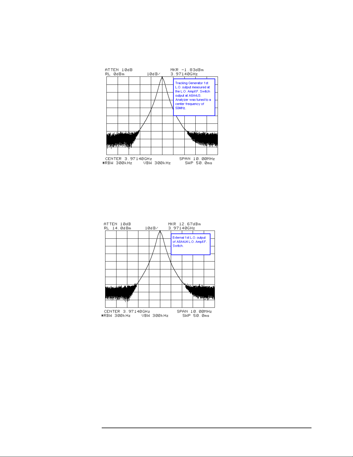
Verifying the RF Section Performance (E4404B, E4405B, E4407B, and
Figure 2-35 Tracking Generator 1st LO - A8A4J4
Troubleshooting the RF Section
E4408B)
Figure 2-36 External 1st LO Output - A8A4
Chapter 2 89
Page 90

Troubleshooting the RF Section
Verifying the RF Section Performance (E4404B, E4405B, E4407B, and
E4408B)
90 Chapter 2
Page 91

3 Block Diagrams
Chapter 3 91
Page 92

Block Diagrams
What You Will Find in This Chapter
What You Will Find in This Chapter
This chapter provides information about the operation of the analyzer that is useful
when first troubleshooting a failure. Refer to the appropriate overall block diagram
at the end of this chapter when reading the assembly descriptions that follow.
These figures show all major assemblies in the analyzer.
The ESA series spectrum analyzers are microprocessor-controlled swept receivers
with frequency ranges from 9 kHz to 1.5 GHz, 3.0 GHz, 6.5 GHz, 13.2 GHz, or
26.5 GHz, depending on the model number. This chapter briefly describes each of
the following analyzer assemblies:
• “A8 1.5 GHz RF Assembly” on page 93
• “A8 RF Assembly” on page 97 which includes:
— “A8J10 Input Connector” on page 98
— “A8A1 3.0 GHz RF Assembly” on page 98
— “A8A1A1 Reference/Third Converter” on page 99
— “A8A1A2 Front End/LO” on page 99
— “A8A2 Second Converter” on page 100
— “A8A3 dc Block” on page 100
— “A8A4 LO Amplifier/IF Switch (LOIS)” on page 100
— “A8A5 Input Attenuator” on page 101
— “A8A6 YIG-Tuned Filter/Mixer (RYTHM)” on page 101
— “A8FL1 3.1 GHz Low-Pass Filter (LPF)” on page 101
— “A7A4 Frequency Extension” on page 101
• “A3 IF Assembly” on page 102
• “A4 Processor Assembly” on page 104
• “A5 Power Supply Assembly” on page 108
• “A1 Display/Front Panel” on page 110
All of the board assemblies listed above are connected to the serial digital interface
through the motherboard connection. All data and control information and all
power supplies, are distributed through these connections. Each of these board
assemblies has its own individual EEPROM with stored serial numbers and
alignment data for the board.
The assemblies listed below do not have individual EEPROMs and are not
connected to the serial digital interface.
• “A7 Motherboard” on page 109
• “A6 Speaker/Floppy Board Assembly” on page 110
92 Chapter 3
Page 93

Block Diagrams
A8 1.5 GHz RF Assembly
A8 1.5 GHz RF Assembly
(E4401B and E4411B)
The A8 RF assembly performs the following major functions:
• Provides input protection
• Provides input attenuation
• Converts RF input signals to the 21.4 MHz IF
• Generates first and second local oscillator (LO) signals for down-conversion
• Uses a fractional-N phase-locked loop for first LO stability
• Generates a 10 MHz reference signal
• Generates an internal 50 MHz amplitude reference signal and a 21.4 MHz IF
alignment signal
The RF section uses a two-stage frequency conversion to convert RF signals to the
21.4 MHz final IF.
Input Connector
The input connector is mounted directly on the RF assembly. This connector can
be easily replaced without disassembling the RF section. Refer to Chapter 6 for the
removal procedure.
Input Protection
CAUTION Exposing the analyzer to high levels of input power over a prolonged time period
can damage the circuitry.
The analyzer input circuitry can be damaged by power levels that exceed the
maximum safe input level specifications. Refer to the analyzer specifications for
the exact values.
Some input protection is provided by a dc-blocking capacitor after the input
connector. The input relay that switches between input signals and an internal
50 MHz alignment signal also functions as an overload protection switch. The
relay is driven by an overload detector that has two power trip points. When the
input attenuation is less than 15 dB, the trip point is approximately +13 dBm
(68 dBmV with Option 1DP) to protect the mixer. When the input attenuation is
15 dB or greater, the trip point is set to approximately +33 dBm (76 dBmV with
Option 1DP) to protect the attenuator.
Chapter 3 93
Page 94

Block Diagrams
A8 1.5 GHz RF Assembly
During an overload condition, the input signal will still be displayed, but at a lower
amplitude. This condition is accompanied by a message displayed on screen
informing the operator of the overload. Refer to the user’s guide for your analyzer
for information on how to clear the overload condition.
Attenuator
The input attenuator provides 0 to 60 dB of attenuation in 5 dB steps. To select
10 dB attenuation, press
Preset.
Low-Pass Filter
The input signal passes through a 1.5 GHz low-pass filter (LPF) to eliminate
unwanted signals above 1.5 GHz.
First Mixer
The first mixer converts incoming signals to a 2.4214 GHz first IF by mixing the
input signal with a 2.4214 to 3.9214 GHz first local oscillator (LO). This LO is
derived by tripling the output from an 800 to 1308 MHz fractional-N phase-locked
loop (PLL) synthesizer.
First IF Amplifier/Filter/Attenuator
The overall gain of the front end is set by the digital-to-analog converter
(DAC)-controlled RF variable gain amplifier. The variable gain amplifier has an
input LPF, input attenuator, amplifier, output attenuator, and an output LPF. The
LPFs provide rejection of harmonics of the LO in order to attenuate unwanted
spurious signals. The two attenuators control the approximately 30 dB of available
gain. This range is used to provide an overall gain of 0 dB from the RF input to the
21.4 MHz output to the IF assembly.
Second Mixer
The second mixer converts the 2.4214 GHz first IF to a 21.4 MHz second and final
IF, by mixing it with a 2.4 GHz second LO. The second LO is derived by tripling
the frequency of an 800 MHz voltage-controlled oscillator (VCO).
94 Chapter 3
Page 95

Block Diagrams
A8 1.5 GHz RF Assembly
21.4 MHz Amplifier
The 21.4 MHz amplifier has 3 functions:
• A bandpass filter (BPF) at the input, to reject signals at 10.7 MHz
• An amplifier, with a typical gain of 12 dB
• A PIN switch circuit, to switch between the IF and the 21.4 MHz IF alignment
signal that is generated by the first LO
Frequency Reference
The 10 MHz voltage-controlled crystal oscillator (VCXO) frequency reference is
used to phase-lock the 800 to 1308 MHz PLL first LO, and the 800 MHz PLL
second LO. It is also used for synchronization with the processor assembly for the
analog-to-digital converter (ADC).
An optional oven-controlled crystal oscillator (OCXO) is also available on the
E4401B as option 1D5. Option 1D5 adds a small board, A8A1 OCXO, to the basic
A8 RF assembly. Cables interconnect A8A1 to A8.
LO
First LO
The 2.4214 to 3.9214 GHz first LO signal is derived from an 800 to 1308 MHz
PLL synthesized signal that is tripled by a diode tripler/filter.
This first LO multiplier consists of three tripler/filter paths that are selected by PIN
diode switches. Each path contains its own tripler/filter and the appropriate signal
path is switched-in based on the desired LO frequency. The three paths are
identical except for the range of their bandpass filters.
The output of the tripler is bandpass-filtered to remove the harmonics, and then
sent to the output switch. It is then amplified with a limiting amplifier, before
going to the first LO amplifier to drive the input mixer.
For frequency sweeps that cross over more than one path range, the two adjacent
paths are enabled simultaneously during band crossings to produce a
“make-before-break” type of switching action. This action is controlled by the
system processor to avoid first LO power drop outs.
The first LO generates the 21.4 MHz IF alignment signal by dividing the PLL
output by 40 and bandpass filtering the divided-down signal.
Chapter 3 95
Page 96

Block Diagrams
A8 1.5 GHz RF Assembly
Second LO
The 2.4 GHz second LO signal and the 50 MHz alignment signal are both
synthesized from the 800 MHz VCO that is phase-locked to the 10 MHz reference.
The 2.4 GHz signal is derived by multiplying the 800 MHz signal with the use of a
tripler/filter path similar to the one used to generate the first LO signal. The
50 MHz amplitude reference signal is derived by dividing the 800 MHz signal by
16.
A8A1 OCXO (Option 1D5)
The A8A1 OCXO (oven-controlled crystal oscillator) provides improved
frequency accuracy and stability. A8A1 receives power and control via A8J2. The
OCXO output is fed back to A8 via A8J4.
Interconnections to Other Assemblies
The A8 RF assembly has three external connectors, (two at the rear of the analyzer
and one at the front). It also has seven internal connectors, (four on the top of the
board, two on the bottom, and one on the bandpass filter (BPF) cavity).
A8J10 RF Input (front external port)
A8J12 EXT REF IN - accepts an external frequency source to provide
the 10 MHz, 15 to +10 dBm frequency reference used by the
analyzer. (rear external port)
A8J3 21.4 MHz IF output to the A3 IF Assembly (internal)
A8J11 EXT REF OUT - provides a 10 MHz, 0 dBm minimum,
time-based reference signal. (rear external port)
A8J5 First LO VCO test port (internal)
A8J6 Second LO VCO test port (internal)
A8J13 BPF alignment port (internal)
A8J4 OCXO 10 MHz REF INPUT from A8A1
A8J2 OCXO (A8A1) power and control (Option 1D5)
Unused
A8J7 (internal)
96 Chapter 3
Page 97

Block Diagrams
A8 RF Assembly
A8 RF Assembly
(E4402B, E4403B, E4404B, E4405B, E4407B, and E4408B)
The A8 RF assembly performs the following major functions:
• Provides input attenuation
• Provides tracking preselection when tuned above 2.85 GHz
• Converts RF input signals to the 21.4 MHz IF
• Generates first, second and third local oscillator (LO) signals for up-conversion
and down-conversion
• Uses a fractional-N phase-locked loop for first LO stability
• Generates a 10 MHz reference signal
• Generates a 50 MHz amplitude reference signal, and an internal 21.4 MHz IF
alignment signal
• Provides an auxiliary first LO output and a 600 MHz signal to drive the
optional 3.0 GHz tracking generator
When tuned below 3.0 GHz, the RF section up-converts the signal to a 3.9214 GHz
first IF, and then down-converts it to a 321.4 MHz second IF, and finally to a 21.4
MHz third IF. When tuned above 3.0 GHz, the RF section down-converts the signal
directly to the 321.4 MHz second IF and then to the 21.4 MHz third IF.
The RF Section consists of four board assemblies, and three microcircuits. Two of
the board assemblies (A8A1A1 and A8A1A2) comprise the A8A1 3.0 GHz RF
Assembly. Not all microcircuits and board assemblies are used in every model.
Refer to the following table.
Chapter 3 97
Page 98

Block Diagrams
A8 RF Assembly
Description
A8A1 3.0 GHz RF Assembly
(includes A8A1A1 and A8A1A2)
A8A1A1 Reference/Third Converter (part of
A8A1 3.0 GHz RF Assembly)
A8A1A2 Front End/LO
(part of A8A1 3.0 GHz RF Assembly)
A8A2 Second Converter X X X
A8A3 DC Block X X X
A8A4 LO Amplifier/IF Switch (LOIS) X X
A8A5 Input Attenuator X X
A8A5 Input Attenuator with Switchable
dc Block
A8A6 YIG-Tuned Filter/Mixer (RYTHM) X X
A8FL1 3.1 GHz Low-Pass Filter (LPF) X X X
E4402B and
E4403B
XXX
XXX
XXX
(Option UKB)
only
E4404B
and
E4405B
X (Option UKB)
E4407B
and
E4408B
only
A7A4 Frequency Extension X X
A8J10 Input Connector
The input connector is mounted to the middle shield of the 3.0 GHz RF assembly.
This connector can be easily replaced without disassembling the RF section. Refer
to Chapter 6 for the removal procedure.
A8A1 3.0 GHz RF Assembly
The A8A1 3.0 GHz RF Assembly is comprised of two boards, the A8A1A1
Reference/Third Converter and the A8A1A2 Front End/LO, in the same shield set.
The A8J10 input connector and the Amptd Ref Out connector (part of the
A8A1W4 50 MHz Amptd Ref Signal), also mount to A8A1. Refer to the following
descriptions for “A8A1A1 Reference/Third Converter” and “A8A1A2 Front
End/LO.”
98 Chapter 3
Page 99

Block Diagrams
A8 RF Assembly
A8A1A1 Reference/Third Converter
(Part of the A8A1 3.0 GHz RF Assembly)
The standard frequency reference is a 10 MHz VCXO. Option 1D5 adds on
oven-controlled crystal oscillator (OCXO). The frequency reference is used to
phase-lock a 100 MHz VCXO. This 100 MHz signal is divided by two to yield the
50 MHz amplitude reference signal, and is tripled to provide the 300 MHz third
LO.
The 300 MHz third LO is then doubled to yield a 600 MHz signal which is the
reference for the first LO and will be used by the A8A2 Second Converter to
generate the 3.6 GHz second LO.
The second IF amplifiers provide approximately 24 dB of gain. There is also a
400 MHz low-pass filter and a 321.4 MHz bandpass filter before the third mixer.
The third mixer is an active mixer, which includes an IF amplifier. The third mixer
down-converts from 321.4 MHz to 21.4 MHz. A variable gain stage, controlled by
a DAC, follows the third mixer. The gain is set to provide 10 dBm output at
A8A1A1P5 when a 10 dBm signal is applied to the analyzer input with 0 dB
input attenuation.
The third IF amplifier is followed by a switch to allow the 21.4 MHz alignment
signal from A8A1A2 to be routed to the A3 IF Assembly for performing automatic
IF alignments between sweeps. Either the output of the third amplifier or the
21.4 MHz alignment signal is routed to the A3 IF Assembly.
A8A1A1 also provides power and control signals for the A8A5 Input Attenuator
and the A8A2 Second Converter.
A8A1A2 Front End/LO
(Part of the A8A1 3.0 GHz RF Assembly)
A limiter at the A8A1A2 input protects the first mixer from excessive RF signals.
A switch following the limiter allows the 50 MHz amplitude reference signal to be
switched-in to perform automatic RF alignments. A preamplifier (available as
Option 1DS on E4401B, E4402B, E4404B, E4405B, and E4407B analyzers) can
be switched-in just before the first mixer. The first mixer is an active mixer with
LO and IF amplifiers. A 700 MHz wide bandpass filter follows the first mixer. The
variable gain first IF amplifier corrects for conversion losses in the front end.
Chapter 3 99
Page 100

Block Diagrams
A8 RF Assembly
The first LO uses a YIG-tuned oscillator in a fractional-N phase-locked loop
(PLL). The 600 MHz reference from A8A1A1 is divided by 128 or 129
dual-modulus prescaler and the resulting ~4.66 MHz signal is used as the reference
for the fractional-N PLL. The 21.4 MHz alignment signal is generated by dividing
the first LO signal by 64 and then limiting the divided signal. The first LO signal
drives a series of three directional couplers. The first directional coupler is used to
drive an ALC loop to level the first LO signal. The second directional coupler
provides feedback for the fractional-N PLL. The last directional coupler provides
an auxiliary first LO output for driving either the optional 3.0 GHz tracking
generator or the A8A4 LO Amplifier/IF Switch (LOIS), which then provides a first
LO signal for the A8A6 YIG-Tuned Filter/Mixer (RYTHM).
A8A2 Second Converter
The A8A2 Second Converter down-converts the 3.9214 GHz first IF to a 321.4
MHz second IF. In high band, it passes the 321.4 MHz first IF from A8A4
(E4404B, E4405B, E4407B, and E4408B) to the A8A1A1 Reference/Third
Converter. The converter generates a 3.6 GHz second LO by multiplying a 600
MHz reference. Bandpass filters remove unwanted harmonics of the 600 MHz
driving signal. First IF and second LO signals are filtered by cavity filters, which
are not user adjustable.
A8A3 dc Block
The dc block protects the input circuitry. It begins to roll off below 9 kHz, the low
frequency limit of the analyzers. A8A3 is not present in analyzers with
Option UKB.
A8A4 LO Amplifier/IF Switch (LOIS)
(E4404B, E4405B, E4407B, and E4408B)
The A8A4 LO Amplifier/IF Switch (LOIS) amplifies the auxiliary LO output from
A8A1A2 and levels the output, as necessary, to provide the optimum first LO
amplitudes to the A8A6 YIG-Tuned Filter/Mixer (RYTHM). An output is also
provided to drive the A2 3.0 GHz tracking generator (Option 1DN). An additional
levelled output is available for External Mixing (Option AYZ).
The IF switch routes the 321.4 MHz IF signal from A8A6 and amplifies it before
passing it along to the A8A7 Second Converter. The IF switch also allows for an
external 321.4 MHz IF input. A dc bias can be applied to the external IF input
signal.
The A8A4 LO Amplifier/IF Switch is controlled by the A7A4 Frequency
Extension assembly.
100 Chapter 3
 Loading...