

Page 1

Addendum A - SERVICE MANUAL
Agilent Technologies Model E4350B and E4351B Solar Array Simulators - P/N 5962-8233
For units with serial numbers:
E4350B US37410101 and up
E4351B US37430101 and up
Foreword
This addendum contains information for troubleshooting and repairing the Agilent E4350B and E4351B
Solar Array Simulators. The standard Service Manual for the Agilent Series 665xA DC Power Supplies (P/N
5959-3376), together with this Service Addendum, is shipped with the Solar Array Simulators when ordered
with Option 910.
Note This addendum is to be used along with the standard Service Manual for the Agilent Series 665xA
DC Power Supplies. When troubleshooting the Agilent E4350B/E4351B Solar Array Simulators,
start by following the procedures outlined in the standard Service Manual. This addendum
documents only the differences between the standard troubleshooting procedures and the
troubleshooting procedures for a Solar Array Simulator.
Areas of Difference
From a service point of view, the main difference between the SAS unit and the Agilent Series 665xA dc
power supply is the addition of a Digital Signal Processor (DSP) board located over the main A1 board. This
DSP board includes the portions of CV, CC, OV, and OC control circuits such as the programming DAC
circuits, as well as a microprocessor and programmable gate array that is used to generate the output I-V
curve. The output I-V curve simulates the output characteristics of a solar array.
The areas in the standard service manual that are changed by this addendum are:
• Test Equipment Required (Table 2-1)
• Basic Test Setup (Figure 2-1)
• Voltage and Current Values (Table 2-3)
• CC RMS Noise Measurement Setup (Figure 2-3)
• Performance Test Record (Table 2-15)
• Self-Test Error Codes/Messages (Table 3-2)
• Troubleshooting Flowcharts (Figures 3-2, 3-5 through 3-9)
• Initialization Program Listing (Figure 3-17)
• Cable and Connector Locations (Figure 3-18)
• Disassembly Procedures for A5 DSP Board (page 3-50)
• Digital Signal Processor (DSP) Board (page 4-14)
• Simplified Power/Control/DSP Circuits (Figure 4-9)
• Parts list (Tables 5-6, 5-7, 5-9 through 5-12)
• Test Points (Table 6-3)
• Schematic Diagrams (Figures 6-5, 6-6, 6-7, 6-10, 6-11, 6-12)
S1
Service Addendum 1
Page 2

Table of Contents
Addendum A - SERVICE MANUAL................................................................................................................................1
Foreword........................................................................................................................................................................1
Areas of Difference........................................................................................................................................................1
Table of Contents...........................................................................................................................................................2
Chapter 1 Differences.....................................................................................................................................................3
Chapter 2 Differences.....................................................................................................................................................3
Test Equipment Required...........................................................................................................................................3
Measurement Techniques...........................................................................................................................................4
Basic Test Setup.........................................................................................................................................................4
Voltage and Current Values.......................................................................................................................................5
Transient Recovery Time...........................................................................................................................................5
CC RMS Noise Measurement Test Setup..................................................................................................................5
Performance Test Record...........................................................................................................................................6
Chapter 3 Differences.....................................................................................................................................................8
Signature Analysis .....................................................................................................................................................8
Self-Test Error Codes/Messages................................................................................................................................8
Overall Troubleshooting (sheet 1)..............................................................................................................................9
Overall Troubleshooting (sheet 2)............................................................................................................................10
Overall Troubleshooting (sheet 3)............................................................................................................................11
Overall Troubleshooting – sheet 4...........................................................................................................................12
Overall Troubleshooting (sheet 5)...........................................................................................................................13
Flow Charts -............................................................................................................................................................13
No Display Troubleshooting....................................................................................................................................14
OV Will Not Fire Troubleshooting..........................................................................................................................15
OV at Turn-On Troubleshooting..............................................................................................................................16
Output Held Low Troubleshooting (sheet 1)...........................................................................................................17
Output Held Low Troubleshooting (sheet 2)............................................................................................................18
Output Held High Troubleshooting..........................................................................................................................19
Initialization and Factory Preset Replacement Program Listing (sheet 1) ...............................................................20
Initialization and Factory Preset Replacement Program Listing (sheet 2) ...............................................................21
Initialization and Factory Preset Replacement Program Listing – (sheet 3)............................................................22
Cable and Connector Locations ............................................................................................................................... 23
Chapter 4 Differences...................................................................................................................................................25
Digital Signal Processor (DSP) Board .....................................................................................................................25
Simplified Diagram of DSP Circuits........................................................................................................................26
Chapter 5 Differences...................................................................................................................................................27
Chapter 6 Differences...................................................................................................................................................43
Test Points................................................................................................................................................................43
Figure 6-5. A1 Main Board Component Location Coordinates for E4350B................................................................47
Figure 6-5. A1 Main Board Assembly Drawing and Test Points for E4350B.............................................................47
Figure 6-5. A1 Main Board Schematic Diagram for E4350B (sheet 1 of 4)................................................................47
Figure 6-5. A1 Main Board Schematic Diagram for E4350B (sheet 2 of 4)................................................................47
Figure 6-5. A1 Main Board Schematic Diagram for E4350B (sheet 3 of 4)................................................................47
Figure 6-5. A1 Main Board Schematic Diagram for E4350B (sheet 4 of 4)................................................................47
Figure 6-6. A4 Left Tunnel Circuit Component Loca tions for E4350B ...................................................................... 47
Figure 6-6. A4A1/A4A3 Left Tunnel Circuit Schematic Diagrams for E4350B.........................................................47
Figure 6-7. A4 Right Tunnel Circuit Component Locations for E4350B....................................................................47
Figure 6-7. A4A2/A4A4 Right Tunnel Circuit Schematic Diagrams for E4350B.......................................................47
Figure 6-10 A5 DSP Board Test Points.......................................................................................................................47
Figure 6-11 A6 Adapter Board Schematic Diagram....................................................................................................47
Figure 6-12 A7 Phone Adapter Board Component Location and Schematic Diagram................................................47
Service Addendum2
Page 3

Chapter 1 Differences
Firmware Revisions
The Agilent E4350B/E4351B SAS firmware resides in the front panel board’s ROM chip (A3U4), the GPIB
board’s ROM chip (A2U106), and in the DSP board’s ROM chips (A5U734 and A5U735).
Use the *IDN query as described in chapter 3 of the Service Manual to get the firmware revision numbers.
Chapter 2 Differences
Test Equipment Required
Table 2-2. Test Equipment Required for Verification
Type Required Characteristics Recommended Model
Current Monitor Resistor 15A (0.1 Ohm) +/- 0.04% Guildline 9230/15
DC Power Supply 5V @ 10A Agilent 6642A, 6653A
Digital Voltmeter Resolution: 10 nV @ 1 V
Readout: 8 1/2 digits
Accuracy: 20 ppm
Electronic Load Voltage and current range must
exceed range of supply under test.
Power range: 500 W min.
GPIB Controller Full GPIB capabilities HP Series 300
Load Resistor
(for CC rms ripple and noise tests)
Oscilloscope Sensitivity: 1 mV
RMS Voltmeter True rms bandwidth: 20 MHz
Variable-Voltage Transformer Adjustable from -13% to +6% of
2 – 16 Ohm 300W (adjusted for 15
Ohm each connected in parallel or
series)
1 – 1.6 Ohm 300W
Bandwidth limit: 20 MHz
Probe: 1:1 with RF tip
Sensitivity: 100 uV
input range.
Power: 1 kVA min.
Agilent 3458A
Agilent 6050A mainframe with
Agilent 60504A (60 V) plug-in
module, or Agilent 60504A-J10 (120
V) plug-in module.
Ohmite E300K16R
Ohmite E300K1R6
Agilent 54504A
Agilent 3400B
Superior Electric
0 to 280 Vac, 7.5 A (226U)
0 to 140 Vac, 15 A (126U)
Service Addendum 3
Page 4

Measurement Techniques
Note All tests are performed in the FIXED as shown in Figure 2-1.
• Measure the DC voltage directly at the +S and -S terminals.
• Set the SENSE switch at the back of the supply to the Remote position.
• Connect the remote sensing leads from +OUT to +S, and from -OUT to -S.
• Use adequate wire gauge for the load leads as described in Chapter 4 of the Operating Manual.
Basic Test Setup
TO OSCILLOSCOPE
OR RMS VOLTMETER
VP I P
IM-IMIP
-
+240 VDC MAX
+
-
S
+
+S-
LOCAL
REMOTE
SET TO
REMOTE
+
120 uF, 100 V
+
-
*
ELECTRONIC
LOAD
CURRENT MONITORING
RESISTOR
(GUILDLINE 0.1 OHM,
15 A, 0.04%)
* USE DC POWER SUPPLY
(SAME POLARITY CONNECTIONS)
FOR -CC TEST
Figure 2-1. Basic Test Setup
TO DVM
TO DVM OR
RMS VOLTMETER
(CC TESTS)
Service Addendum4
Page 5

Voltage and Current Values
Table 2-3. Voltage and Current Values
Agilent Model Full-scale
Voltage
E4350B
E4351B
60V 61.5V 8A 8.16A 73.0V
120V 123V 4A 4.08A 140V
Max. Prog.
Voltage
Full-scale
Current
Transient Recovery Time
This test does not need to be performed on the Agilent E4350B.
CC RMS Noise Measurement Test Setup
IM-IM
-
+240 VDC MAX
-
IP
VP I P
+
-
+
+S-
S
I
Max. Prog.
Current
LOCAL
REMOTE
Max. Prog.
Overvoltage
SET TO
REMOTE
MONITOR
RESISTOR 1.6 OHM
(Adjusted to 1 Ohm +/- 1%)
LOAD RESISTOR
E4350B 2 16 Ohm resistors in parallel
(Adjusted to 7 Ohms +/- 1%)
E4351B 2 16 Ohm resistors in series
(Adjusted to 25 Ohms +/- 1%)
Figure 2-3. CC RMS Noise Measurement Test Setup
Service Addendum 5
RMS
VOLTMETER
Page 6
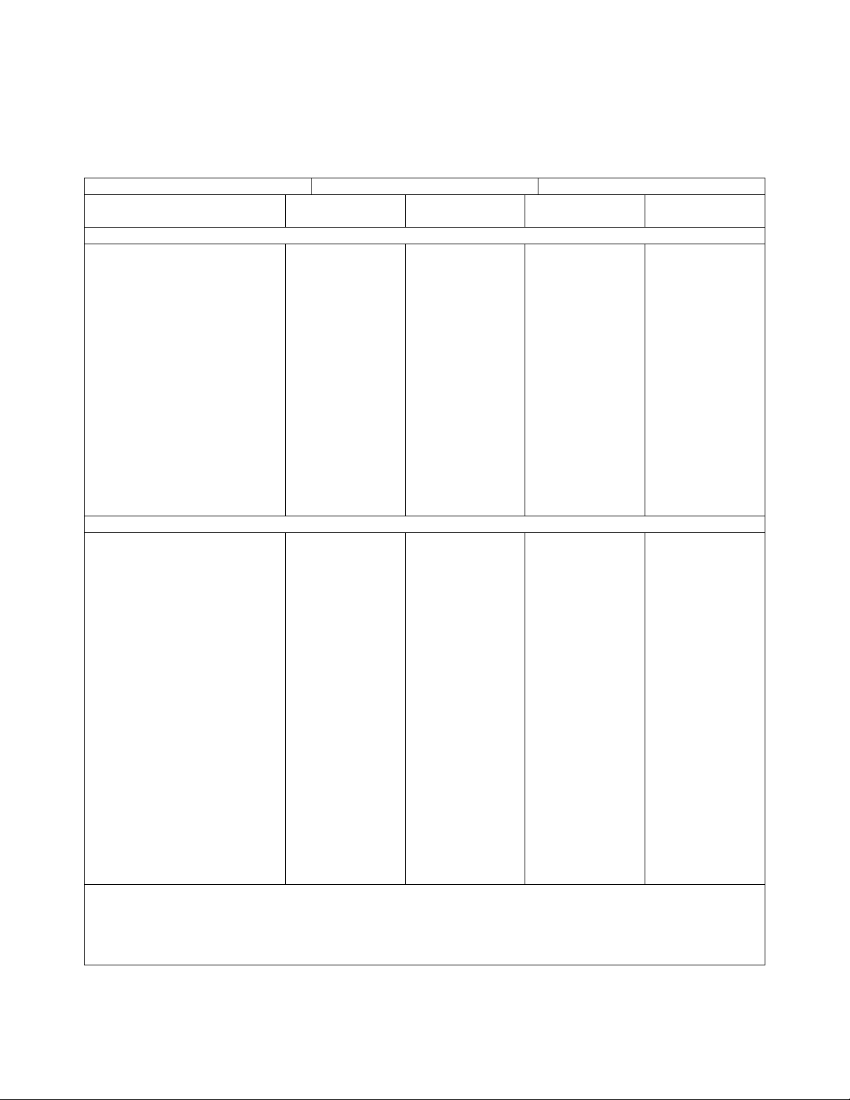
Performance Test Record
Table 2-15A. Performance Test Record for Agilent Model E4350B
Agilent E4350B Report No.______________ Date _________________
Test Description Minimum Spec. Result * Maximum Spec. Measurement
Uncertainty
Constant Voltage Tests
Voltage Programming and
Readback Accuracy
Low Voltage (set to 0V) V
Readback Accuracy
out1
V
out1
-10mV
– 42mV
_________ mV
_________ mV
V
out1
+10mV
+ 42mV
1.5µV
2µV
High Voltage (set to 60V) V
out2
Readback Accuracy
Load Effect
Source Effect
PARD (Ripple & Noise)
Peak to Peak
RMS
Current Programming and
Readback Accuracy
Low Current (set to 0A) Iout1
Readback Accuracy
High Current (set to 8A) Iout2
Readback Accuracy
Current Sink (Isink = 1.8A)
Readback Accuracy
PARD (Ripple & Noise)
RMS
SAS Mode **
RMS
Peak to Peak
59.945V
V
out2
– 2mV
– 2mV
– 90mV
0
0
__________ V
_________ mV
_________ mV
_________ mV
_________ mV
_________ mV
60.055V
V
out2
+ 2mV
+ 2mV
95mV
12mV
+ 90mV
Constant Current Tests
– 20mA
I
– 28mA
out1
7.964A 8.036A
– 44mA
I
out2
Isink – 54mA Isink + 54mA
0
0
0
_________ mA
_________ mA
__________ A
_________ mA
_________ mA
_________ mA
_________ mA
_________ mA
V
out1
V
out2
+20mA
+ 28mA
+ 44mA
2.4mA
4mA
32mA
845µV
845µV
40µV
40µV
840µV
2.1mV
0.5µA
20µA
3.3mA
3.3mA
1mA
1.8mA
270µA
2.6mA
Load Effect
Source Effect
– 1mA
– 1mA
_________ mA
_________ mA
+ 1mA
+ 1mA
* Enter your results in this column
** PARD (Optional Test in SAS mode)
Program I – V Curve: I
= 8A I
SC
= 7.5A V
MP
= 60V V
MP
= 65V RL = 8 Ohms.
OC
Use Fig 2-3 with scope across monitoring resistor for P-P ripple or RMS voltmeter for RMS.
Service Addendum6
3.4µA
3.4µA
Page 7

Table 2-15B. Performance Test Record for Agilent Model E4351B
Agilent E4351B Report No.______________ Date _________________
Test Description Minimum Spec. Result * Maximum Spec. Measurement
Uncertainty
Constant Voltage Tests
Voltage Programming and
Readback Accuracy
Low Voltage (set to 0V) V
Readback Accuracy
out1
V
out1
-20mV
– 84mV
_________ mV
_________ mV
+20mV
V
out1
+ 84mV
1.7µV
1.7µV
High Voltage (set to 120V) V
out2
Readback Accuracy
Load Effect
Source Effect
PARD (Ripple & Noise)
Peak to Peak
RMS
Current Programming and
Readback Accuracy
Low Current (set to 0A) Iout1
Readback Accuracy
High Current (set to 4A) Iout2
Readback Accuracy
Current Sink (0.9A) Readback
Accuracy
PARD (Ripple & Noise)
RMS
SAS Mode **
RMS
Peak to Peak
119.89V
V
– 180mV
out2
– 2mV
– 2mV
0
0
Constant Current Tests
– 10mA
I
– 14mA
out1
3.982A
I
– 22mA
out2
Isink – 27mA
0
0
0
__________ V
_________ mV
_________ mV
_________ mV
_________ mV
_________ mV
_________ mA
_________ mA
__________ A
_________ mA
_________ mA
_________ mA
_________ mA
_________ mA
120.11V
V
+ 180mV
out2
+ 2mV
+ 2mV
95mV
12mV
+ 10mA
+ 14mA
V
out1
4.018A
V
+ 22mA
out2
Isink + 27mA
2.4mA
4mA
32mA
1.7mV
1.7mV
230µV
230µV
3mV
1.5mV
16µA
16µA
0.6mA
0.6mA
120µA
270µA
270µA
2.6mA
Load Effect
Source Effect
– 1mA
– 1mA
_________ mA
_________ mA
+ 1mA
+ 1mA
* Enter your results in this column
** PARD (Optional Test in SAS mode)
Program I – V Curve: I
= 4A I
SC
= 3.75A V
MP
= 120V V
MP
= 130V RL = 32 Ohms.
OC
Use Fig 2-3 with scope across monitoring resistor for P-P ripple or RMS voltmeter for RMS.
Service Addendum 7
2.2µA
2.2µA
Page 8

Chapter 3 Differences
Signature Analysis
Signature analysis (SA) troubleshooting for the secondary circuits on the A1
main circuit board is ++NOT++ available for the Agilent E4350B unit. However,
GPIB and front panel signature analysis is available as described
in chapter 3 of the Service Manual.
Self-Test Error Codes/Messages
Code/Message Description Probable Cause
Table 3-2. Self-Test Error Codes/Messages
E1 FP RAM
E2 FP ROM
E3 EE CHKSUM
E4 PRI XRAM
E5 PRI IRAM
E6 PRI ROM
E7 GPIB
E8 SEC RAM
E9 SEC ROM
E10 SEC 5 V
E11 TEMP
E12 DACS
E30 SEC DAC
E31 SEC DAC
E32 SEC DAC
E45 SEC IO
E46 SEC NVRAM
Front panel RAM test failed
Front panel ROM test failed
Front panel EEPROM checksum failed
Primary interface external RAM test failed
Primary interface internal RAM test failed
Primary interface DOM test failed
GPIB interface test failed
Secondary interface RAM test failed
Secondary interface ROM test failed
Secondary interface 5 volt readback test failed
Ambient temperature readback test failed
CV or CC DAC test failed
Secondary interface DAC test failed
Secondary interface DAC test failed
Secondary interface DAC test failed
Secondary interface I/O test failed
Secondary interface nonvolatile RA M test fail ed
Microprocessor A3U3 defective
ROM A3U4 or address latch A3U8 defective
Possibly due to power loss during a write operation. See
checksum Error Recovery on page 3-3 in the Operating
manual. If power loss is not the problem, EEPROM A3U6
could be defective (after replacing U6, supply must be
initialized and calibrated).
A2 GPIB board defective
A2 GPIB board defective
A2 GPIB board defective
Talker/Listener chip A2U117 defective
A5 DSP board defective
A5 DSP board defective
A5 DSP board defective
A5 DSP board defective
A5 DSP board defective
A5 DSP board defective
A5 DSP board defective
A5 DSP board defective
A5 DSP board defective
A5 DSP board defective
Note: The following error messages can appear due to a failure occurring either while the power supply is operating or during self test.
SERIAL TIMEOUT
SERIAL DOWN
UART PARITY
UART FRAMING
UART OVERRUN
SBUF OVERRUN
SBUF FULL
STK OVERFLOW
EE WRITE ERR
SECONDARY DN
Serial data line failure on GPIB board
Serial data line failure on GPIB board
Uart failed on GPIB board
Uart failed on GPIB board
Uart failed on GPIB board
Serial buffer failure on GPIB board
Serial buffer failure on GPIB board
Stack overflow failure on DSP board
EEPROM write failure on front panel board
Serial data line failure on DSP board
A2 GPIB board defective
A2 GPIB board defective
A2 GPIB board defective
A2 GPIB board defective
A2 GPIB board defective
A2 GPIB board defective
A2 GPIB board defective
A5 DSP board defective
EEPROM A3U6 defective or calibration error
A5 DSP board defective
Service Addendum8
Page 9

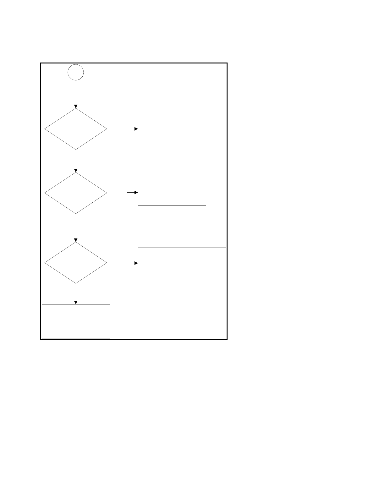
Overall Troubleshooting (sheet 1)
Start "Overall
Troubleshooting"
Turn off supply, disconnect
the load and push the sense
switch on the rear panel in
(local). Turn on the supply
Display On?
Yes
Fan on?
No No
Fan On?
Yes
Go to "No Display"
Troubleshooting
No
1. Check ac input and line cord
2. Check line fuse
3. Turn off supply, remove top cover, check line
voltage select jumpers on T1.
4. Tur n on supply, chec k ac power and ac bias
voltages at T1 secondary
Turn off the supply and remove top cover to access
the A1 board. Turn on the supply and check voltage
at heatsink of A1Q770 (TP 12) with respect to
common (TP 9). See Fig 6-5 Sheet 1.
Yes
Error message
displayed
?
No
Using front panel keys, program full
scale voltage and current. Check the
voltage at the supply’s output
terminals with a DMM.
Output voltage
within spec
?
Yes
Yes
See "Self Test Error
Codes/Messages",
Table 3-2
No
B
To Sheet 4
1. Check ac bias voltage at T1
secondary and cable W7. See Fig
6-2 in 665xA service manual.
A1Q700 Heatsink
+24V?
Yes
1. Check Fan B1 and cable connection to A1J601
2. Check fan speed control circuit A1Q700, A1U702
and associated components. See Fig 6-5 sheet 1.
No
2. Check A1F700, 701, D702705, C711 and R709.
A
To Sheet 2
Figure 3-2. Overall Troubleshooting (sheet 1 of 5)
Service Addendum 9
Page 10

Overall Troubleshooting (sheet 2)
From Sheet 1
A
Voltage display
within spec
?
No
Reads approx. right
but outside spec
Check cables from A1
A5J722-1 (Vmon)
No
?
approx. 4.1V
?
YesYes
No
main board to A5 DSP
board.
Yes
CV
Annunciator
on ?
Yes
Turn off the supply and connect a short
across the output terminals. Turn on
and program full scale voltage and
current using front panel keys. Check
output current with an external
ammeter.
Output current
within spec?
Yes
Current display
within spec?
No
Calibrate the supply. See
Appendix A in the Operating
No
No No No
See CV/CC Status Annunciator
Troubleshooting" paragraph
C
manual.
To Sheet4
Reads approx.
right but outside
spec?
Voltage readback circuit on
A5 DSP board defective.
A5J722-3 (Imon)
approx. 4.4V
?
Check cables from A1
Main board to A5 DSP
Yes
CC Annunciator
on ?
Yes
D
To Sheet3
Yes Yes
Calibrate supply. See Appendix A in
the Operating manual.
Current readback circuit on
No
A5 DSP board defective
Current readback circuit on
A5 DSP board defective
Figure 3-2. Overall Troubleshooting (sheet 2 of 5)
Service Addendum10
Page 11

Overall Troubleshooting (sheet 3)
D
From Sheet 3
Turn off the supply and remove the short from the
output. Turn on and program output voltage and
current to full scale and the OV to zero using front
panel keys. Check that the supply goes into OV
condition (OV Prot annunciator on and output at 0)
Did OV occur?
Yes
Turn off the supply and connect a GPIB
controller to the supply. Turn on the supply and
using the controller, program the supply to full
scale voltage and current. Check that the supply
accepts the commands and can be programmed
down rapidly.
Does supply accept
commands ?
Yes
Down Programming
OK
?
No
Go to "Slow Down Programming"
troubleshooting Fig. 3-15
No
No
Go to "OV Will Not Fire"
Troubleshooting
1. Check GPIB cable
2. Check A2J115, J117 and J120
Yes
Check Primary Interface A2
U113, U114, U118.
Check operation of the Digital Control Port
(See Appendix A of the Operating manual),
Serial Link (See Chapter 4 in Operating
manual) and the front panel voltage/current
rotary controls (See Chapter 5 in the Operating
No
manual).
Digital Control Port
OK
?
Yes
Check A2U109, U114.
Check Voltage and Current
controls (A3G1 & G2).
No
No
No problem found. Perform
Verification tests in Chapter 2 to
determine if a problem exists
Figure 3-2. Overall Troubleshooting (sheet 3 of 5)
Service Addendum 11
Serial Link
OK
?
Yes
Rotary Controls OK
?
Yes
Page 12

Overall Troubleshooting – sheet 4
B From Sheet 1
C
From Sheet 2
Output voltage
approx. right but
outside spec
?
No
PROT
annumciator on
?
Yes
Press PROT key
Calibrate the supply. See Appendix
A in the Operating manual.
No
Display reads
approx. output
voltage
?
Yes
Display reads
approx. 0 Amps
?
Yes
Check Voltage Monitor
No
No
circuit A1U605
Output shorted
Check Current Monitor
circuit A1U605
YesYes
No
Output current
approx. right but
outside spec
?
No
Check output for
Yes
?
shorted circuits
No
Yes
Display reads
approx. output
current
?
OT
displayed
?
No
E
Output low
?
No
Go to "Output Held Low"
troubleshooting.
Yes Yes
Go to Sheet 5
Go to "Output Held Low"
Yes
A5J722-31
Therm Heatsink
3.2V @ 23C
Check +5V Ref,
A1R510,right tunnel board
A4RT301 (10K @ 23C)
Figure 3-2. Overall Troubleshooting (sheet 4 of 5)
troubleshooting.
Replace A5 DSP board
?
No
Service Addendum12
Page 13
Overall Troubleshooting (sheet 5)
E From Sheet 4
Programmable OCP tripped, Check
OV & OC
displayed
?
No
Yes
OC circuits A1U405, U411, Imon
amp A1U403 and OC_PROG signal
at A5J722-26 (TP41)
OV
displayed
?
No
OC
displayed
?
No
RI (Remote Inhibit)
displayed? Check for short
between A2TB101 and
ground.
Figure 3-2. Overall Troubleshooting (sheet 5 of 5)
Yes
Yes
Go to "OV at Turn-On"
troubleshooting.
Check if OCP is enabled at turn-on
and current is programmed to zero.
Check current circuit.
Flow Charts -
The flow charts shown in Figures 3-10 through Figures 3-14 and Figure 3-16 are not used
in troubleshooting the Solar Array Simulator.
Note that there are no changes to the flow chart in Figure 3-15.
Service Addendum 13
Page 14

No Display Troubleshooting
"No Display"
Start
Turn on the supply and try to program it from the
front panel. While measuring the voltage at the
output terminals, program the voltage and current to
full scale. Toggle the ON/OFF key while observing
the external voltmeter.
No display but output
OK
?
Yes
Turn off supply, remove front panel
assembly to access circuits on the A3 front
panel board. Turn on the supply.
Check 5V bias at R1-6, display voltages:
1.1V at R1-14, 2.2V at R1-2 and 3.3V at
R1-16 (meter common at R1-3). See Fig.
6-4.
Display and bias
voltages OK
?
Yes
Check 10MHz Clock signal at
A3J2-9. See Fig. 6-9.
No
Check the A2 GPIB board, bias circuits,
No
PCLR (test points 1 - 4 Table 6-3) and
cable W9
Check A3C1,
A3R1 and A3RT1.
Yes
Program voltage and current fron the front
panel. Measure the voltage at the output
terminals. In case the output is disabled
press the output ON/OFF key while
observing the output with an external
voltmeter.
Display and bias
voltages OK
?
A3U3, A3U4 or A3U8
Check A3Y1,
No
A3C3, A3C4 and
A3U3.
defective. Perform
front panel SA. See
Table 3-4.
Figure 3-5. No Display Troubleshooting
Service Addendum14
Output Voltage present
No
LCD or cable W19 defective.
?
Yes
Page 15

OV Will Not Fire Troubleshooting
"OV Will Not Fire"
Start
Turn off supply and remove top cover. Turn on
and check secondary bias and reference
voltages. (Test Points 9 through 17, Table 6-3)
Voltages OK
?
Yes
Program voltage and current to full scale and
OV to 1/2 full scale. Check voltage at A5 J72222 (TP40), A1U405 and A1U602 with respect
to common (TP9).
J722-22 approx. 2.7V
?
Yes
A1U405-7 approx. 0V
?
Yes
No
Troubleshoot the appropriate
defective circuit.
Replace A5 DSP boardNo
No
Check A1R644, R747 and C417.
Voltage at A1U603-7 should be
approx. 2V.
Check voltage at A1U405-5 with
respect to common (TP9)
Yes
No
A1U405-5 Negative
?
A12U602-6 approx.
5V
?
Yes
Check voltage across A1R516
Yes
A1U602-6 approx. 5V
?
Yes
Check A1Q701 and CR700.
Check A5 J721-12. If not 5V,
No
replace A5 DSP board. If 5V
check A1U602 and DSP cable.
No
Check A1U410, Q701
(B-E short?)
Figure 3-6. OV Will Not Fire Troubleshooting
Service Addendum 15
Yes
Check A1U405.
Page 16

OV at Turn-On Troubleshooting
"OV at Turn-On"
Start
Check that the supply is not programmed to OV at
turn-on. Ensure that the voltage setting is not greater
than the OV setting. Program 0V and Max. OV, then
save the settings in Register 0 (press shift, save, 0
and Enter key). Turn the supply off then back on.
Connect a DC coupled scope across the output
terminals. Turn the supply on and check that the
output does not momentarily go higher than the
voltage setting.
Momentarily goes high
Turn off the supply and remove the top cover.
Disable the OV circuit by lifting A1R447. Turn on
the supply and check the output voltage.
?
Yes
Output high
?
Yes
Caution: During
these tests, the
output may be at
hazardous levels.
Yes
Go to "Output Held High"
Troubleshooting
Yes
OV still ocurrs
?
Check voltages at A1U405-7 (TP44), U603-5 (TP17,
U405-5 (TP42) and U405-3 (TP41) to Common
(TP9). See Table 6-3.
A1U405-7 approx 5V
?
Yes
Yes
Figure 3-7. OV at Turn-on Troubleshooting
Check A1R447,
R446, C417
Check A1U411.
No
Check A1U405.
Check A1R644,
C417.
Yes
Yes
A1U405-7 approx 5V
A1U405-7 approx 5V
Replace A5 DSP board
?
No
?
No
Service Addendum16
Page 17

Output Held Low Troubleshooting (sheet 1)
"Output Held Low"
Start
The supply’s output is low and the PROT
annunciator is not on. Turn supply off, disconnect
the load and remove the top cover. Turn the supply
on and check the secondary bias and reference
voltages (TP’s 9 through 12 See Table 6-3).
Voltages OK
?
Yes
Check that the +Rail and -Rail Voltages
are correct. See Fig. 6-5, Sheet 1.
Rail Voltages OK
?
Yes
Program full scale voltage and current, measure
output with an external DMM to insure the problem
is no a power supply readback problem. Check
voltages is approximately -4 volts at A5J722-15
(TP25) and A5J722-16 (TP24) with respect to
commmon (TP9).
No
No
Caution: During
these tests, the
output may be at
hazardous levels.
Troubleshoot the defective
curcuit. See Fig. 6-5 Sheet 1.
Check power xfmr T1 ac
voltages, input rectifiers and
filter caps. See Fig. 6-5 Sheet 1
Voltages OK
?
Yes
Check if CV/CC "OR" Gate diodes
A1D441 or D413 are conducting.
A1D411 Conducting
?
No
A
To Sheet 2
Figure 3-8 Output Held Low Troubleshooting (Sheet 1 of 2)
Replace A5 DSP Board
No
Check Vmon voltage at
A1U401-7 (TP33) to
common (TP9).
Yes
Yes
CV Comparator
A1U408
A1D411 Conducting
?
No
VMon Amp A1U401
defective
Service Addendum 17
Page 18

Output Held Low Troubleshooting (sheet 2)
From Sheet 1
A
No
A1D413 Conducting
?
Yes
Check voltage at A1U408-3 and
R686 (TP36) to common (TP9).
A1U408-3 Neg
?
No
A1R638 > 12mV
?
Yes
Check if supply operates OK with
no load but cannot get full scale
output with load connected.
Yes
Check IMon voltage at A1U403-7
(TP28) to common (TP9).
A1D413 Conducting
?
No
IMon Amp A1U403 defective.
Gross Current Limit circuit A12U409
Yes
No
Check A1U408, D420, loading of
voltage by Tunnel Circuits.
defective.
Disconnect cables from tunnel boards
A4A1-A4A4 one at a time to see if
output rises.
Yes
CC Comparator A1U403 defective.
Partial output attained
?
No
Check Gated +9V and Shutdown
circuit. See Test Points 18-21, Table
6-3 and Figure 6-5 Sheet 2.
Figure 3-8 Output Held Low Troubleshooting (Sheet 2 of 2)
Output Rises
No
Check A1U408 and D420
Disconnect cables from Tunnel
boards one at a time to see if one has
Yes
little or no effect. Troubleshoot or
replace the defective board.
Service Addendum18
Troubleshoot or replace defective
Yes
?
tunnel board.
Page 19

Output Held High Troubleshooting
"Output Held High"
Start
Turn supply off and remove the top cover. Disable
the Overvoltage circuit by shorting A1U410 pins1 &
2 and lifting A1R447. Turn the supply on and check
the secondary bias and reference voltages (TP’s 9
through 12 See Table 6-3).
Caution: During
these tests, the
output may be at
hazardous levels.
Voltages OK
?
Yes
Program voltage and current to 1/2 full scale. Check
voltage at A5J722-15 (TP25) and A5J722-16 (TP24)
to common (TP9). Voltages should be
approximately -2V.
Voltages OK
?
Yes
Check if CV "OR" gate diode A1D411 is conducting.
A1D411 Conducting
?
Yes
Check output control voltage at
A1R638 (TP36) to common (TP9).
A1R638 approx. 12mV
?
No
No
No
Troubleshoot the defective
curcuit. See Fig. 6-5 Sheet 1.
Replace A5 DSP board
Check A1U408, D411
Yes
Yes
Load output to 5% rated current
*
and check drop across emittor
resistors on left boards A4A1 &
A4A2 (R201, R206, R216) and
on right boards A4A2 & A4A4
(R301, R306, R311, R316) to
help isolate defective stage (see
Fig 6-6 and 6-7). A defective
stage will be conducting more
current.
Disconnect cables from Top
Tunnel boards A4A1 and
A4A2.
Output OK
?
No
Reconnect top tunnel
boarda and disconnect
cables from Top Tunnel
boards A4A3 and A4A4.
No
Check A1U408, U409
Reconnect Tunnel boards
one at a time to isolate
defective board.*
Yes
Check A1U408. Voltage at
A1R511 should be >8V.
Figure 3-9. Output Held High Troubleshooting
Service Addendum 19
Output OK
?
No
Page 20

Initialization and Factory Preset Replacement Program Listing (sheet 1)
10 ! Program to initialize EEPROM data in Models E4350B and E4351B
20 ! RE-STORE "INIT_435X"
30 ! Rev A.00.00 dated Nov, 17,1998
40 !
50 DIM Init_data(1:49),Model$[6],Idn$[21]
60 INTEGER Addr(1:49),Length(1:49)
70 ASSIGN @Ps TO 705 ! Supply must be at address 705
80 CLEAR SCREEN
90 !
100 Eprom_data_addr: ! Data address
110 DATA 2,6,10,14,18,19,20,24,28,32
120 DATA 36,37,38,42,46,50,54,55,56,57
130 DATA 64,68,72,76,80,84,88,92,96,100
140 DATA 136,137,138,139,140,142,146,148,149,150
150 DATA 151,152,153,154,155,156,157,158,160
160 !
170 Eprom_data_len: ! Data for word length
180 DATA 4,4,4,4,1,1,4,4,4,4
190 DATA 1,1,4,4,4,4,1,1,1,1
200 DATA 4,4,4,4,4,4,4,4,4,4
210 DATA 1,1,1,1,2,4,2,1,1,1
220 DATA 1,1,1,1,1,1,1,2,1
230 !
240 Eprom_data_50B: ! ! EEPROM data for E4350B
250 DATA 56.71,76.42,61.5,0,82,0,409.6,148.05,8.16,0
260 DATA 99,3,9.321,27,73,0,83,255,20,10
270 DATA 4350,54.39,167,436.44,167,0,10.0,10.0,65,1600
280 DATA 5,255,0,0,17,4350,0,20,160,20
290 DATA 160,156,37,98,115,15,20,0,96
300 !
310 Eprom_data_51B: ! ! EEPROM data for E4351B
320 DATA 28.36,40.96,123.0,0,0,82,0,819.2,283.57,4.08,0
330 DATA 99,3,5.121,27,140,0,83,255,20,10
340 DATA 4351,27.19,167,872.89,167,0,5.0,5.0,130,400
350 DATA 5,255,0,0,17,4351,0,20,160,20
360 DATA 160,156,37,98,115,15,20,0,96
370 !
380 RESTORE Eprom_data_addr
390 !
400 FOR I=1 TO 49
410 READ Addr(I)
420 NEXT I
430 !
440 RESTORE Eprom_data_len
450 !
460 FOR I=1 TO 49
470 READ Length(I)
480 NEXT I
490 !
500 INPUT "Input the model number (i.e. E4350B)",Model$
Figure 3-17. Initialization and Factory Preset Replacement Program Listing (Sheet 1 of 3)
Service Addendum20
Page 21

Initialization and Factory Preset Replacement Program Listing (sheet 2)
510 CLEAR SCREEN
520 !
530 SELECT Model$
540 CASE "E4350B"
550 RESTORE Eprom_data_50B
560 CASE "E4351B"
570 RESTORE Eprom_data_51B
580 CASE ELSE
590 DISP "Error in Model number, must be E4350B or E4351B."
600 STOP
610 END SELECT
620 !
630 FOR I=1 TO 49 ! Read model dependent data
640 READ Init_data(I)
650 NEXT I
660 !
670 OUTPUT @Ps;"*CLS" ! Clears power supply registers
680 !
690 OUTPUT @Ps;"CAL:STATE ON," ! Turn on cal mode, "0" passcode
700 !
710 GOSUB Ps_error ! Error if passcode is not "0"!
720 IF Err THEN
730 OUTPUT @Ps;"*IDN?" ! Get data from model # location
740 ENTER @Ps;Idn$
750 Model=VAL(Idn$[POS(Idn$,",")+2])
760 ELSE
770 GOTO Start
780 END IF
790 !
800 OUTPUT @Ps;"CAL:STATE ON,";Model ! Turn on cal mode, passcode =
810 ! data at model number location
820 !
830 GOSUB Ps_error ! Error if passcode is not same as
840 ! data at model # location
850 IF Err THEN
860 OUTPUT @Ps;"CAL:STATE ON,";Model$[1,4] ! Turn on cal mode, passcode =
870 ! model #
880 GOSUB Ps_error
890 IF Err THEN
900 PRINT "Change pass code to the power supply model # or zero then restart the program."
910 STOP
920 ELSE
930 GOTO Start
940 END IF
950 END IF
960 !
970 Start: !
980 !
990 CLEAR SCREEN
1000 PRINT "Initializing EEPROM"
Figure 3-17. Initialization and Factory Preset Replacement Program Listing (Sheet 2 of 3)
Service Addendum 21
Page 22

Initialization and Factory Preset Replacement Program Listing – (sheet 3)
1010 !
1020 FOR I=1 TO 49
1030 OUTPUT @Ps;"DIAG:EEPR ";Addr(I);",";Length(I);",";Init_data(I)
1040 NEXT I
1050 !
1060 CLEAR SCREEN
1070 OUTPUT @Ps;"CAL:STATE OFF" ! Turn off cal mode
1080 !
1090 GOSUB Ps_error ! Check for errors
1100 IF Err THEN
1110 PRINT "An error occurred during the EEPROM read/write, Check for"
1120 PRINT "programming errors. Initialization data may be incorrect."
1130 STOP
1140 END IF
1150 !
1160 PRINT "Operation complete. Program stopped."
1170 STOP
1180 !
1190 Ps_error: ! Error handling subroutine
1200 OUTPUT @Ps;"SYST:ERR?" ! Check for errors
1210 ENTER @Ps;Err
1220 RETURN
1230 !
1240 END
Figure 3-17. Initialization and Factory Preset Replacement Program Listing (Sheet 3 of 3)
Service Addendum22
Page 23

Cable and Connector Locations
A2 GPIB
Board
A6 J900
A6 Adapter PCA
J722
A5 DSP
Board
J721
A7 Phone PCA
A1 J900
A1 Main
Board
A4A3
A4A1
Left
Tunnel
Board
A4A2
Right
Tunnel
Board
A4A4
A3 Front Panel Board
Figure 3-18. Cable and Connector Locations for E4350B/E4351B
Service Addendum 23
Page 24

DSP Board
To remove the A5 DSP Board, proceed as follows:
• Remove the top cover of the power supply as described under, "Top Cover Removal and
Replacement."
• Remove the six screws that attach the cover to the DSP board (use a T10 TORX drive).
• Disconnect both cables going to the GPIB board.
Note Be sure to mark any or all cables prior to removal so that no mistake is made later when reinstalling
these cables.
• Disconnect the ribbon cable located at the end of the DSP board.
• Remove the two screws that attach the DSP board to the left side of the chassis
(Use a T10 TORX drive).
• Lift the DSP board together with its mounting bracket out of the chassis.
• Disconnect the cable going to the front panel board.
• Turn the DSP board over and remove the screws that attach the DSP board
to the mounting bracket.
Service Addendum24
Page 25

Chapter 4 Differences
Digital Signal Processor (DSP) Board
The DSP board replaces the Secondary Interface section of the A1 Main PC board. It replaces the
Secondary Microprocessor (U504), the CV and CC programming DACs, Readback D/A, DAC Reference,
Readback Comparators, and the Fan and Overvoltage PWMs. It replaces everything found in Figure 6-5,
sheet 3 plus the OV filter/buffer (U603) found on sheet 2.
The DSP board contains the new Secondary Microprocessor circuits, the CV, CC, OV, OC and Fan DAC’s,
The readback circuits and the secondary ROM and RAM. When operating in the Fixed mode, the instrument
acts like a normal power supply with typical crossover characteristics between CV and CC operation. When
in SAS mode the customer specified I/E operating curve is entered into the secondary RAM where it is used
to modify the supply’s crossover characteristics.
Troubleshooting is to be performed in the Fixed (turn-on default) mode only. See Figure 6-10 for the
A5J721/A5J722 connector DAC and Bias voltage pin-outs.
Note The DSP board is available as a replacement assembly only. It is not intended to be repaired to the
component level.
The following figure is a simplified diagram that shows the circuits located on the DSP board (also referred
to as the Secondary Interface) in relation to the Output Power and Control circuits previously discussed in
chapter 4.
Service Addendum 25
Page 26
Simplified Diagram of DSP Circuits
ross
+ G
t
u
S
O
+
+
25K
406
407
9K
408
R
+
R490
10K
ontrol
C
V
C
125K
401B
U
SAS
408B
U
p
m
ontrol A
C
0 to -5V
703
R
0.02
it
urrent Lim
C
1
R
R
-
+
491
R
411
D
408A
U
404
9K
R
Fixed
10K
-
+
S
SA
r
O
ate
V
G
C
488
R
409A
U
- S
- Out
P.O. DSP Board
CV_ Prog
CV
DAC
Monitor
Output Voltage
Fixed
4.99K
+5V
Amp
Down
Programming
DAC
IMon
CC_ Prog
CC
DAC
U773
Ref
+5V
Data
U752
U750
A/D
U753
A/D
U751
VMon
n
o
S
A
M
S
V
412
200
411
R
4.99K
R
401A
U
434
900
to -5V
433
410
464
R
426
C
.047uF
0
R
432
20K
440
R
463
R
R
4.64K
urrent
onitor
M
utput C
O
2K
ontrol
C
C
C
+ 15V
497
R
31.6K
5V
+
503
R
R
900
-
435
+
20K
R
605A
U
465
10K
R
-
403A
U
13
4
D
19
4
D
+
409B
U
14.7K
I Mon
+
Gate
CC Or
-
503
R
4.12K
-
+
202
U
-
+
201
ly
b
ssem
A
ink
t S
ea
. H
.O
P
Q201
Series Regulator
S
D
ail
+ R
U
202
Q
G
in
V
er
n
m
ow
D
Program
Figure 4-9. Simplified Power/Control/DSP Circuits
Service Addendum26
Q206
Q205
PLD
uP
U736
U710
Sch4350.Pre
- Rail
Page 27

Chapter 5 Differences
Table 5-6. Parts List for E4350B/E4351B Chassis
Reference
Designator Model Part Number Description
A1 E4350B E4350-61024 Main PC Board
A1 E4351B E4351-61021 Main PC Board
A2 5063-4851 GPIB Board
A3 5063-2360 Keypad/Front Panel PC Board
A4A2 & A4A4 5063-4816 Right Tunnel PCA
A4A1 5063-4818 Left Top Tunnel PCA
A4A3 5063-4820 Left Bottom Tunnel PCA
A5 5063-4811 DSP Board
A6 5063-4852 Access Panel PCA
A7 5063-4813 Phone PCA
W1A 06652-80006 Cable-Assembly, AC #1
W1B 06652-80007 Cable-Assembly, AC #2
W2 06654-80001 Cable-Assembly, Xfmr
W3 06654-80003 Cable-Assembly, Rail
W7 06652-80009 Cable Assembly, AC Bias
W8 06652-80008 Cable, GPIB Bias
W9 06652-80011 Cable-Phone, A2 to L Tunnel
W10 5080-2168 Cable-Phone, A2 to A3
W11, 15 06652-80010 Cable-Phone, A1 to L Tunnel
W13, 17 06652-80011 Cable-Phone, A1 to R Tunnel
W12, 16 06652-80001 Cable-Assembly, A1 to L Tunnel
W14, 18 06652-80002 Cable-Assembly, A1 to R Tunnel
W19 5080-2261 Cable-Assembly, LCD
W20 5080-2419 Ribbon Cable, A1 to A6
Chassis –Mechanical
Front Panel Logo E4350-80003 Nameplate E4350B
Front Panel Logo E4351-80002 Nameplate E4351B
Ref J690 0360-2191 Cover-Term Block
Ref G1, G2 0370-1091 Knob-Base Round
Ref Rmt/Lcl Switch 0370-2862 Pushbutton
Ref GPIB Connector 0380-644 Threaded Stud
Ref Front Frame 0515-0374 Screw-M3x0.5
0515-0375 Screw-Machine
Ref Cover PCB, A5 Board 0515-0380 Screw-M4x0.7
0515-0382 Screw-Machine
Ref Xfmr Bracket 0515-0413 Screw-M4x0.7
Ref Term Block Cover 0515-1085 Screw-Machine
Ref Top Cover 0515-1132 Screw-M5x0.8
0515-1455 Screw-Thd Rlg
Ref A5 Cover, A6 Board 0515-0430 Screw-Torx #10
Ref Fan Top Shroud 0535-0031 Nut-Hex W/Lkwr
Ref Shroud To Base, AC Gnd 0535-0082 Nut-Hex
Ref Display 0590-0534 Nut, Self Thd
06652-00004 Cover, Top
Ref Heatsink 06652-00008 Heatsink Shroud
Ref A4 Top & Bottom 06652-20001 Heatsink
Ref T1 06652-60005 Jumper Assembly
Service Addendum 27
Page 28

Table 5-6. Parts List for E4350A Chassis-Mechanical (continued)
Reference
Designator Part Number Description
Ref Display 1000-0842 Window
Ref A2TB101 1252-1488 Terminal Block, 4-Pos
Ref A1J640 1252-3698 Connector
Ref Ac Bias, Tunnel Cables 1400-0493 Cable Tie
Ref Front Bracket 1400-0528 Mount-Cable Tie
Ref Ac Pwr, Tunnel 1400-1281 Clip-Cable
Ref Rear Panel Ground 1510-0044 Binding Post-Single
Ref GPIB Board 1531-0309 Clevis
Ref F450 2110-0927 Fuseholder-W/Cap
2190-0016 Washer-Lk Intl T
2190-0034 Washer-Lk Hlcl
Ref AC Ground 2190-0646 Washer-Lock
2950-0043 Nut-Hex-Dbl-Cham
Ref GPIB Connector 3050-0849 Washer-Fl Mtlc
5001-0539 Trim-Sides
5001-6734 Front Panel
5001-6740 Bracket-GPIB
5001-6748 Front Panel
5001-6771 Rear Panel
5001-9819 Chassis
5040-1665 Keypad
5040-1666 Heat Sink-Rail
5040-1667 Heat Sink-Bumper
5040-1697 Block-Top Cover
5040-1703 Front Frame
5041-8801 Foot
5041-8819 Cap-Strap Handle, Front
5041-8820 Cap-Strap Handle, Rear
5062-3704 Strap Handle
Ref Serial Link Cable 5080-2148 Cable, Chain-2m.
5959-3376 Guide, Service
5960-5597 Guide, Programming
5961-2579 Guide, Operating
5962-8206 SAS Operating Guide
Ref A5 DSP Board E4350-00001 Bracket-Mounting
Ref A5 DSP Board E4350-00002 Cover
Front Panel Logo E4350-80003 Nameplate E4350B
Front Panel Logo E4351-80002 Nameplate E4351B
Service Addendum28
Page 29

Table 5-7. Parts List for Main PC Board Assembly (A1)
Reference
Designator Model Part Number Description
A1 E4350B E4350-61024 Main Board – Electrical
A1 E4351B E4351-61021 Main Board – Electrical
C401 E4350B 0160-4835 Capacitor .1uF 10% 50V
C401 E4351B 0160-4834 Capacitor.047UF 10%
C402 E4350B 0160-4835 Capacitor .1uF 10% 50V
C402 E4351B 0160-4834 Capacitor.047UF 10%
C403 E4350B 0160-4807 Capacitor 33pF 5% 100V
C404 E4350B 0160-4807 Capacitor 33pF 5% 100V
C405 0160-5422 Capacitor.047 uF 20%
C406 0160-4812 Capacitor 220 pF 5%
C407 0160-5422 Capacitor .047 uF 20%
C408 0160-5422 Capacitor .047 uF 20%
C409 0160-4800 Capacitor 120pF 5%
C410 0160-4800 Capacitor 120pF 5%
C411 0160-5422 Capacitor .047 uF 20%
C412 0160-4800 Capacitor 120pF 5%
C413 0160-4800 Capacitor 120pF 5%
C414 0160-6616 Capacitor 6800pF 100V
C415 0160-5909 Capacitor 0.047uF 50 V
C416 0160-5422 Capacitor .047 uF 20%
C417 0160-4812 Capacitor 220pF 5%
C418 0160-4831 Capacitor 4700pF 10%
C419 0160-4831 Capacitor 4700pF 10%
C420 0160-4812 Capacitor 220pF 5%
C421 0160-5098 Capacitor .22uF 10%
C422 0180-4129 Capacitor 1uF 35V
C423 E4350B 0160-5422 Capacitor .047 uF 20%
C424 0160-5422 Capacitor .047 uF 20%
C425 0160-5422 Capacitor .047 uF 20%
C426 0160-5909 Capacitor 0.047uF 50 V
C427 0160-5909 Capacitor 0.047uF 50 V
C428 E4350B 0160-4812 Capacitor 220pF 5%
C428 E4351B 0160-4808 Capacitor470PF 100V
C429 0160-5422 Capacitor.047 uF 20%
C430 0160-4833 Capacitor .022uF 10%
C432 0160-4831 Capacitor 4700pF 10%
C434 0160-5644 Capacitor .033 uF 10%
C435 E4350B 0160-5644 Capacitor .033 uF 10%
C436 0160-5469 Capacitor 1uF 10% 50V
C437 0160-6616 Capacitor 6800pF 100V
C439 0160-4831 Capacitor 4700pF 10%
C440 E4350B 0160-4833 Capacitor .022uF 10%
C440 E4351B 0160-4832 Capacitor.01UF 10%
C441 0160-5422 Capacitor .047 uF 20%
C442 0160-5422 Capacitor .047 uF 20%
C443 E4350B 0160-5422 Capacitor .047 uF 20%
C445 0160-4807 Capacitor 33pF 5% 100V
C446 0160-4801 Capacitor 100pF 5%
C447 0160-4805 Capacitor 47pF 5% 100V
Service Addendum 29
Page 30

Table 5-7. Parts List for Main PC Board Assembly A1 (Continued)
Reference
Designator Model Part Number Description
C448 0160-5422 Capacitor .047 uF 20%
C449 0160-4791 Capacitor 10pF 5% 100V
C450 0160-5422 Capacitor .047 uF 20%
C451 E4351B 0160-4832 Capacitor.01UF 10%
C452 0160-4355 Capacitor .01uF 10%
C453 0160-4846 Capacitor 1500pF 100V
C454 0160-5422 Capacitor .047 uF 20%
C455 0180-4129 Capacitor 1uF 35V
C456 0160-4805 Capacitor 47pF 5% 100V
C457 0160-4831 Capacitor 4700pF 10%
C458 0160-4787 Capacitor 22pF 5% 100V
C459 0160-4832 Capacitor .01uF 10%
C541 E4350B 0160-4832 Capacitor .01uF 10%
C601 E4350B 0160-6806 Capacitor .1uF 400V
C601 E4351B 0160-4323 Capacitor .047uF 250V
C603 0160-4795 Capacitor 4.7pF
C604 0160-5422 Capacitor .047 uF 20%
C605 0160-5422 Capacitor .047 uF 20%
C606 0160-4800 Capacitor 120pF 5%
C607 0160-5422 Capacitor .047 uF 20%
C608 0160-4801 Capacitor 100pF 5%
C609 0180-0197 Capacitor 2.2uF 20V
C610 0160-4835 Capacitor .1uF 10% 50V
C611 0160-4800 Capacitor 120pF 5%
C700 0160-4281 Capacitor 2200pF 20%
C701 0160-4281 Capacitor 2200pF 20%
C702 0160-7606 Capacitor 1uF 275V
C703 0160-4845 Capacitor 6800pF 20%
C704 0160-4355 Capacitor .01uF 10%
C705 0180-4129 Capacitor 1uF 35V
C706 0180-4129 Capacitor 1uF 35V
C707 0160-4830 Capacitor 2200pF 10%
C709 E4350B 0160-6804 Capacitor .047uF 250V
C709 E4351B 0160-6896 Capacitor0.015uF 400V
C710 0160-6896 Capacitor 0.015uF 400V
C711 0160-4834 Capacitor .047uF 10%
C712 0180-4132 Capacitor 6.8uF 35V
C713 0180-3458 Capacitor 4700uF 50V
C714 0180-3458 Capacitor 4700uF 50V
C715 0180-3458 Capacitor 4700uF 50V
C715 E4351B 0160-5422 Capacitor.047 UF 20%
C716 0160-4904 Capacitor 6800pF 5%
C718 0160-5469 Capacitor 1uF 10% 50V
C719 E4350B 0180-4263 Capacitor 4000uF 125V
C719 E4351B 0180-4311 Capacitor1200UF 250V
C720 E4350B 0180-4263 Capacitor 4000uF 125V
C720 E4351B 0180-4311 Capacitor1200UF 250V
C721 E4350B 0180-3497 Capacitor 6800uF 16V
Service Addendum30
Page 31

Table 5-7. Parts List for Main PC Board Assembly A1(Continued)
Reference
Designator Model Part Number Description
C722 E4351B 0180-4311 Capacitor1200UF 250V
C722 E4350B 0180-4263 Capacitor 4000uF 125V
C723 0160-0168 Capacitor .1uF 10%
C724 0160-5422 Capacitor .047 uF 20%
C725 E4350B 0160-5422 Capacitor .047 uF 20%
CR700 5060-3376 SCR/Diode Assembly
D401 1901-0033 Diode
D402 1901-0033 Diode
D403 1901-0033 Diode
D404 1901-0033 Diode
D405 1901-0033 Diode
D406 1901-1128 Diode
D407 1901-1128 Diode
D408 1901-0033 Diode
D409 1901-0033 Diode
D410 1901-1098 Diode
D411 1901-1098 Diode
D413 1901-1098 Diode
D415 1901-0518 Diode
D416 1901-0050 Diode
D417 1901-0050 Diode
D418 1901-0033 Diode
D419 1901-1098 Diode
D420 1901-1098 Diode
D421 1901-1098 Diode
D422 1901-0050 Diode
D423 1901-0050 Diode
D424 1901-1098 Diode
D425 1901-1098 Diode
D426 1901-0050 Diode
D427 1901-0050 Diode
D428 1901-0731 Diode
D429 1901-0731 Diode
D430 1901-0050 Diode
D431 1901-0050 Diode
D601 1901-0050 Diode
D602 1901-0050 Diode
D603 1901-0050 Diode
D604 1901-0050 Diode
D605 1901-0050 Diode
D606 1901-0731 Diode
D607 1901-0050 Diode
D608 1901-0050 Diode
D609 1901-1214 Diode
D700 1901-1098 Diode
D701 1901-1098 Diode
D702 1901-0719 Diode
D703 1901-0719 Diode
D704 1901-0719 Diode
D705 1901-0719 Diode
Service Addendum 31
Page 32

Table 5-7. Parts List for Main PC Board Assembly A1 (Continued)
Reference
Designator Model Part Number Description
D706 1901-1098 Diode
D707 1901-0992 Diode
D709 1906-0383 Full Wave Rectifier
D710 1901-1087 Diode
D711 1901-1087 Diode
D712 1901-0050 Diode
F700 2110-0685 Fuse, Subminiature, 7A
F701 2110-0685 Fuse, Subminiature, 7A
F703 2110-0688 Fuse, 3A 125V
F704 2110-0697 Fuse, Subminiature, 15A
F705 2110-0697 Fuse, Subminiature, 15A
J405 1251-4781 Connector
J411 1251-4781 Connector
J450 1251-7616 Connector
J451 1252-3771 AC Line Module
J600 1251-4246 Connector, TP
J601 1251-4245 Connector, 2 pin
J640 1252-3693 Connector
J670 1251-8184 Modular Phone Rcpt
J671 1251-8184 Modular Phone Rcpt
J672 1251-8184 Modular Phone Rcpt
J673 1251-8184 Modular Phone Rcpt
J690 06652-00005 Bus Bar
J691 06652-00005 Bus Bar
J900 1251-8601 Connector, TP
L701 5080-2321 Output Choke
Q206 5060-3250 Transistor/Heatsink Assy
Q401 1855-0727 MOSFET
Q402 1853-0281 Transistor
Q403 1854-0872 Transistor
Q600 1853-0336 Transistor
Q601 1853-0336 Transistor
Q602 1853-0336 Transistor
Q603 1853-0336 Transistor
Q604 1854-0575 Transistor
Q605 1855-0727 MOSFET
Q700 5060-3322 Transistor/Heatsink Assy
Q701 1854-0477 Transistor
R401 E4350B 0698-3153 Resistor 3.83K 1%
R401 E4351B 0757-0440 Resistor 7.5K 1%
R402 E4350B 0698-6320 Resistor 5K .1% .125W
R402 E4351B 0698-6360 Resistor 10K .1%
R403 E4350B 0698-6320 Resistor 5K .1% .125W
R403 E4351B 0698-6360 Resistor 10K .1%
R404 0698-5454 Resistor 9K .1% .125W
R405 E4350B 0757-0288 Resistor 9.09K 1%
R406 E4350B 0699-3446 Resistor 125K .05%
R406 E4351B 0699-3104 Resistor 250K .125W
R407 0698-5454 Resistor 9K .1% .125W
Service Addendum32
Page 33

Table 5-7. Parts List for Main PC Board Assembly A1 (Continued)
Reference
Designator Model Part Number Description
R408 E4350B 0699-3446 Resistor 125K .05%
R408 E4351B 0699-3104 Resistor 250K .125W
R409 E4350B 0757-0288 Resistor 9.09K 1%
R410 0698-0082 Resistor 464 1% .125W
R411 0698-3279 Resistor 4.99K 1%
R412 0683-2015 Resistor 200 5% .25W
R413 E4350B 0698-3153 Resistor 3.83K 1%
R413 E4351B 0757-0440 Resistor 7.5K 1%
R414 8159-0005 Resistor-Zero Ohms
R415 0698-6360 Resistor 10K .1%
R416 0698-6360 Resistor 10K .1%
R417 8159-0005 Resistor-Zero Ohms
R418 0698-6630 Resistor 20K .1%
R419 0698-6360 Resistor 10K .1%
R420 0698-6630 Resistor 20K .1%
R421 0698-6630 Resistor 20K .1%
R422 0698-6360 Resistor 10K .1%
R423 0698-6630 Resistor 20K .1%
R424 8159-0005 Resistor-Zero Ohms
R425 0699-0118 Resistor 20K .1% .1W
R426 0698-6362 Resistor 1K .1% .125W
R427 0698-6362 Resistor 1K .1% .125W
R428 0699-0118 Resistor 20K .1% .1W
R429 8159-0005 Resistor-Zero Ohms
R430 8159-0005 Resistor-Zero Ohms
R431 8159-0005 Resistor-Zero Ohms
R432 0699-0118 Resistor 20K .1% .1W
R433 0698-6344 Resistor 900 .1%
R434 0698-6344 Resistor 900 .1%
R435 0699-0118 Resistor 20K .1% .1W
R436 8159-0005 Resistor-Zero Ohms
R437 0699-0533 Resistor 4.64K .1%
R438 0698-3136 Resistor 17.8K 1%
R439 0757-0288 Resistor 9.09K 1%
R440 0699-0533 Resistor 4.64K .1%
R441 E4350B 0699-0088 Resistor 1.2M 1%
R441 E4351B 0698-8826 Resistor 825K 1%
R442 0698-3155 Resistor 4.64K 1%
R443 0757-0446 Resistor 15K 1% .125W
R444 0757-0439 Resistor 6.81K 1%
R445 E4350B 0698-8827 Resistor 1M 1% .125W
R445 E4351B 0699-0070 Resistor3.16M 1%
R446 0698-3260 Resistor 464K 1%
R447 E4350B 0757-0465 Resistor 100K 1%
R447 E4351B 0757-0471 Resistor 182K 1%
R448 0698-0084 Resistor 2.15K 1%
R449 0698-3155 Resistor 4.64K 1%
R450 0757-0446 Resistor 15K 1% .125W
R451 0698-3260 Resistor 464K 1%
R452 0698-6320 Resistor 5K .1% .125W
Service Addendum 33
Page 34

Table 5-7. Parts List for Main PC Board Assembly A1 (Continued)
Reference
Designator Model Part Number Description
R453 0699-0533 Resistor 4.64K .1%
R455 0698-0084 Resistor 2.15K 1%
R456 0757-0401 Resistor 100 1% .125W
R458 0698-3428 Resistor 14.7 1%
R460 0757-0459 Resistor 56.2K 1%
R461 0698-3162 Resistor 46.4K 1%
R462 0698-3162 Resistor 46.4K 1%
R463 0757-0283 Resistor 2K 1% .125W
R464 0698-4435 Resistor 2.49K 1%
R465 0698-6360 Resistor 10K .1%
R466 0757-0430 Resistor 2.21K 1%
R467 E4350B 0757-0270 Resistor 249K 1%
R467 E4351B 0757-0468 Resistor 130K 1%
R468 0698-5454 Resistor 9K .1% .125W
R469 0698-3700 Resistor 715 1% .125W
R471 0757-0401 Resistor 100 1% .125W
R473 0757-0427 Resistor 1.5K 1%
R474 0698-3156 Resistor 14.7K 1%
R475 E4350B 0757-0418 Resistor 619 1% .125W
R475 E4351B 0757-0283 Resistor 221
R476 0698-3156 Resistor 14.7K 1%
R477 8159-0005 Resistor-Zero Ohms
R478 0698-3279 Resistor 4.99K 1%
R479 0698-4435 Resistor 2.49K 1%
R480 E4350B 0757-0418 Resistor 619 1% .125W
R480 E4351B 0757-0282 Resistor 221 1% .125W
R481 0698-3156 Resistor 14.7K 1%
R482 0698-3557 Resistor 806 1% .125W
R483 0757-0279 Resistor 3.16K 1%
R484 0757-0199 Resistor 21.5K 1%
R485 0757-0199 Resistor 21.5K 1%
R488 0698-3279 Resistor 4.99K 1%
R489 E4350B 0757-0451 Resistor 24.3K 1%
R489 E4351B 0757-0457 Resistor 47.5K 1%
R490 0698-6360 Resistor 10K .1%
R491 0698-6360 Resistor 10K .1%
R492 0757-0433 Resistor 3.32K 1%
R493 E4350B 0699-1254 Resistor 536K 1%
R493 E4351B 0698-8827 Resistor 221K 1%
R494 E4350B 0757-0412 Resistor 365 1% .125W
R494 E4351B 0757-0421 Resistor 1M 1% .125W
R495 0757-0434 Resistor 3.65K 1%
R496 0757-0469 Resistor 150K 1%
R497 0698-3160 Resistor 31.6K 1%
R498 0698-3162 Resistor 46.4K 1%
R499 0757-0463 Resistor 82.5K 1%
R500 0757-0407 Resistor 200 1% .125W
R501 0757-1093 Resistor 3K 1% .125W
R502 E4350B 0698-3493 Resistor 4.12K 1%
R502 E4351B 0757-0427 Resistor 1.5K 1%
R503 E4350B 0698-3156 Resistor 14.7K 1%
R503 E4351B 0698-4121 Resistor 11.3K 1%
Service Addendum34
Page 35

Table 5-7. Parts List for Main PC Board Assembly A1 (Continued)
Reference
Designator Model Part Number Description
R504 0757-0442 Resistor 10K 1% .125W
R505 0757-0429 Resistor 1.82K 1%
R506 0698-3160 Resistor 31.6K 1%
R507 0757-0442 Resistor 10K 1% .125W
R508 0757-0444 Resistor 12.1K 1%
R509 0757-0280 Resistor 1K 1% .125W
R510 0698-3279 Resistor 4.99K 1%
R511 0757-0430 Resistor 2.21K 1%
R512 0757-0401 Resistor 100 1% .125W
R513 0757-0401 Resistor 100 1% .125W
R514 0757-0284 Resistor 150 1% .125W
R515 0757-0284 Resistor 150 1% .125W
R516 0698-0084 Resistor 2.15K 1%
R517 0699-1797 Resistor 10M 5% .25W
R520 0757-0419 Resistor 681 1% .125W
R521 0757-0470 Resistor 162K 1%
R522 0757-0442 Resistor 10K 1% .125W
R523 0757-0472 Resistor 200K 1%
R524 0698-8826 Resistor 825K 1%
R525 0698-3156 Resistor 14.7K 1%
R526 0757-0427 Resistor 1.5K 1%
R601 0757-0465 Resistor 100K 1%
R602 0698-4037 Resistor 46.4 1%
R603 0757-0407 Resistor 200 1% .125W
R604 0698-4037 Resistor 46.4 1%
R605 0757-0407 Resistor 200 1% .125W
R606 0698-4037 Resistor 46.4 1%
R607 0757-0407 Resistor 200 1% .125W
R608 E4350B 8159-0005 Resistor-Zero Ohms
R608 E4351B 0757-0463 Resistor 82.5K 1%
R609 0757-0463 Resistor 82.5K 1%
R610 E4350B 0698-0082 Resistor 464 1% .125W
R610 E4351B 0757-0280 Resistor 1K 1% .125W
R611 0698-6358 Resistor 100K .1%
R612 0757-0463 Resistor 82.5K 1%
R613 E4350B 8159-0005 Resistor-Zero Ohms
R613 E4351B 0757-0463 Resistor 82.5K 1%
R614 0698-6358 Resistor 100K .1%
R615 E4350B 8159-0005 Resistor-Zero Ohms
R615 E4351B 0698-6629 Resistor 60K .1%
R616 E4350B 0698-6977 Resistor 30K .1% .125
R616 E4351B 0698-6358 Resistor100K .1%
R617 0698-5454 Resistor 9K .1% .125W
R618 E4350B 0698-8826 Resistor 825K 1%
R618 E4351B 0699-1972 Resistor 1.74M 1%
R619 E4350B 0698-6977 Resistor 30K .1% .125
R619 E4351B 0698-6358 Resistor 100K .1%
R620 0757-0442 Resistor 10K 1% .125W
R621 0757-0415 Resistor 475 1% .125W
R622 0757-0281 Resistor 2.74K 1%
R623 0698-5454 Resistor 9K .1% .125W
Service Addendum 35
Page 36

Table 5-7. Parts List for Main PC Board Assembly A1 (Continued)
Reference
Designator Model Part Number Description
R624 8159-0005 Resistor-Zero Ohms
R625 E4350B 0698-8826 Resistor 825K 1%
R625 E4351B 0699-1972 Resistor 1.74M 1%
R626 8159-0005 Resistor-Zero Ohms
R627 8159-0005 Resistor-Zero Ohms
R628 E4350B 8159-0005 Resistor-Zero Ohms
R628 E4351B 0698-6629 Resistor 60K .1%
R630 0757-0395 Resistor 56.2 1%
R631 0757-0199 Resistor 21.5K 1%
R632 0757-0401 Resistor 100 1% .125W
R633 0757-0469 Resistor 150K 1%
R634 0757-0446 Resistor 15K 1% .125W
R635 0757-0430 Resistor 2.21K 1%
R636 0757-0415 Resistor 475 1% .125W
R637 0757-0415 Resistor 475 1% .125W
R638 0757-0407 Resistor 200 1% .125W
R639 0698-3155 Resistor 4.64K 1%
R640 0698-3155 Resistor 4.64K 1%
R641 0698-3153 Resistor 3.83K 1%
R642 0698-3155 Resistor 4.64K 1%
R643 0698-8695 Resistor 36K .1%
R644 0698-0084 Resistor 2.15K 1%
R645 0757-0442 Resistor 10K 1% .125W
R646 0757-0280 Resistor 1K 1% .125W
R647 0683-0475 Resistor 4.7 5% .25W
R648 0683-0475 Resistor 4.7 5% .25W
R649 0757-0280 Resistor 1K 1% .125W
R650 0757-0441 Resistor 8.25K 1%
R651 0757-0465 Resistor 100K 1%
R652 0698-3160 Resistor 31.6K 1%
R653 0757-0199 Resistor 21.5K 1%
R654 0698-8816 Resistor 2.15 1%
R655 0757-0199 Resistor 21.5K 1%
R656 0757-0199 Resistor 21.5K 1%
R657 0698-3162 Resistor 46.4K 1%
R658 0757-0199 Resistor 21.5K 1%
R659 8159-0005 Resistor-Zero Ohms
R661 0757-0401 Resistor 100 1% .125W
R662 0757-0280 Resistor 1K 1% .125W
R700 0683-1055 Resistor 1M 5% .25W
R701 0699-1797 Resistor 10M 5% .25W
R702 0683-0335 Resistor 3.3 5% .25W
R703 E4350B 0811-3764 Resistor .025 7W 2%
R703 E4351B 0811-3770 Resistor .05 OHM 1%
R704 8159-0005 Resistor-Zero Ohms
R705 0698-6359 Resistor 80K O.1%
R706 0698-6979 Resistor 111.1K .1%
R707 0699-1212 Resistor 19K .1%
R708 8159-0005 Resistor-Zero Ohms
R709 0699-4707 Resistor .25 Ohm
R710 0811-2201 Resistor 270 5% 2W PW
R711 0811-2201 Resistor 270 5% 2W PW
Service Addendum36
Page 37

Table 5-7. Parts List for Main PC Board Assembly A1 (Continued)
Reference
Designator Model Part Number Description
R712 0686-2225 Resistor 2.2K 5% .5W
R713 E4350B 0811-3932 Resistor 13 10W
R714 E4351B 0811-3932 Resistor-13 10W
R716 E4351B 0811-3932 Resistor-13 10W
R717 8159-0005 Resistor-Zero Ohms
R718 0811-2568 Resistor 1 1% 3W PWI
R719 0757-0280 Resistor 1K 1% .125W
R720 0757-0279 Resistor 3.16K 1%
R721 E4350B 0811-1873 Resistor 3K 5% 10W PW
R721 E4351B 0811-1914 Resistor 5K 5% 10W PW
R722 E4350B 0811-1873 Resistor 3K 5% 10W PW
R722 E4351B 0811-1914 Resistor 5K 5% 10W PW
R723 E4350B 0698-3628 Resistor 220 5% 2W MO
R723 E4351B 0698-3627 Resistor 200 5% 2W MO
R724 0698-0082 Resistor 464 1% .125W
R725 E4350B 0811-1586 Resistor 1K 5% 10W PW
R725 E4351B 0811-1873 Resistor 3K 5% 10W PW
R726 8159-0005 Resistor-Zero Ohms
R727 0757-0280 Resistor 1K 1% .125W
R728 0699-4707 Resistor .25 Ohm
R729 0757-0419 Resistor 681 1% .125W
REF D709 E4350B 0515-0383 Machine Screw
REF D709 E4350B 1205-0862 Heat Sink
REF D7092 E4351B 0515-0383 Machine Screw
REF D7094 E4351B 1205-0862 Heat Sink
REF J451 E4350B 3050-0891 Flat Washer
REF J451 E4350B 0535-0031 Hex Nut w/Lock Washer
REF J690, J691 E4350B 2190-0586 Helical Lock Washer
REF J690, J691 E4350B 0515-0909 Machine Screw
REF J451 E4351B 570-0647 STUD-STD-PRS-IN
REF J4512 E4351B 0535-0031 NUT-HEX W/LKWR
REF J4513 E4351B 3050-0891 WSHR-FL MTLC
REF J6902,6912 E4351B 2190-0586 WSHR-LK HLCL
REF J690,J691 E4351B 0515-0909 SCR-MACH MAX .07
S610 3101-2894 Push Button Switch, DPDT
U401 1826-1533 Integrated Circuit
U402 1826-1533 Integrated Circuit
U403 1826-2252 Integrated Circuit
U404 1826-1533 Integrated Circuit
U405 1826-0412 Integrated Circuit
U406 1858-0077 Transistor Array
U407 1826-0175 Integrated Circuit
U408 1826-1533 Integrated Circuit
U409 1826-1533 Integrated Circuit
U410 1990-1502 Opto Isolator
U411 1820-3081 Integrated Circuit
U600 1826-1895 Integrated Circuit
U601 1858-0077 Transistor Array
U602 1858-0047 Transistor Array
U603 1826-0412 Integrated Circuit
Service Addendum 37
Page 38

Table 5-7. Parts List for Main PC Board Assembly A1 (Continued)
Reference
Designator Model Part Number Description
U604 1858-0077 Transistor Array
U605 1858-0076 Transistor Array
U700 5060-3321 IC/Heat Sink Assy
U701 5063-2351 IC/Heat Sink Assy
U702 1826-1533 Integrated Circuit
U703 5063-2328 IC/Heat Sink Assy
VR400 1902-0556 Zener Diode 20V 5%
VR600 1902-0947 Zener Diode 3.6V 5%
VR601 1902-0947 Zener Diode 3.6V 5%
VR602 1902-3104 Zener Diode 5.62V 5%
VR603 1902-0958 Zener Diode 10V 5%
VR700 1902-0957 Zener Diode 9.1 V 5%
VR701 1902-0955 Zener Diode 7.5V 5%
XF450 2110-0927 Fuseholder w/Cap
Table 5-9. Parts List for GPIB PC Assembly (A2)
Reference Designator Part Number Description
A2 5063-2356 GPIB Board (unchanged)
Table 5-10. Parts List for Front Panel PC Assembly (A3)
Reference Designator Part Number Description
A3 5063-2360 Front Panel Board (unchanged)
Service Addendum38
Page 39

Table 5-11. Parts List for Top Left Tunnel Board (A4A1)
Reference
Designator Part-Number Description
A4A1 5063-4818 Top Left Tunnel Board
C201 0160-4801 Capacitor 100PF 5%
C202 0160-4801 Capacitor 100PF 5%
C203 0160-4801 Capacitor 100PF 5%
C204 0160-4801 Capacitor 100PF 5%
C205 0160-4835 Capacitor .1UF 10% 50V
C206 0160-4835 Capacitor .1UF 10% 50V
C208 0160-6838 Capacitor 2200pf 1KV
C211 0160-4812 Capacitor 220PF 5%
D201 1901-1098 Diode
D203 1901-0050 Diode
D204 1901-0050 Diode
D205 1901-0050 Diode
F201 2110-0297 Fuse, 0.5A, 125V
F202 2110-0297 Fuse, 0.5A, 125V
F203 2110-0297 Fuse, 0.5A, 125V
F204 2110-0297 Fuse, 0.5A, 125V
F205 8159-0005 Resistor, Zero Ohms
F206 8159-0005 Resistor, Zero Ohms
F207 8159-0005 Resistor, Zero Ohms
F208 8159-0005 Resistor, Zero Ohms
J201 1251-8184 Modular Phone Rcpt
J202 1251-4781 Connector
Q201 1855-0849 FET
Q203 1855-0849 FET
Q205 1854-0989 Transistor
Q207 1855-0849 FET
Q206 5060-3250 Transistor/Heat Sink Assy
R201 0811-3989 Resistor 1.5 1% 3W
R202 0698-3430 Resistor 21.5 1%
R203 0698-3156 Resistor 14.7K 1%
R204 0757-0280 Resistor 1K 1% .125W
R206 0811-3989 Resistor 1.5 1% 3W
R207 0698-3430 Resistor 21.5 1%
R208 0698-3156 Resistor 14.7K 1%
R209 0757-0280 Resistor 1K 1% .125W
R210 0698-3456 Resistor 287K 1%
R212 0757-0316 Resistor 42.2 1%
R213 0698-3441 Resistor 215 1% .125W
R214 0698-0085 Resistor 2.61K 1%
R215 0698-4503 Resistor 66.5K 1%
R216 0811-3989 Resistor 1.5 1% 3W
R217 0698-3430 Resistor 21.5 1%
R218 0698-3156 Resistor 14.7K 1%
R219 0757-0280 Resistor 1K 1% .125W
R220 0757-0468 Resistor 130K 1%
R221 0757-0280 Resistor 1K 1% .125W
R224 0698-3628 Resistor 220 5% 2W MO
R229 8159-0005 Resistor, Zero Ohms
R230 8159-0005 Resistor, Zero Ohms
R232 8159-0005 Resistor, Zero Ohms
R233 8159-0005 Resistor, Zero Ohms
0340-0458 Insulator (Ref Q205)
0515-0064 Screw, Mach M3x0.5x16mm pan head (Ref Q201,Q203,Q205,Q207)
1200-1158 Transistor Socket (Ref Q201,Q203,Q205,Q207)
2190-0584 Washer, helical lock (Ref Q201,Q203,Q205,Q207)
Service Addendum 39
Page 40

Table 5-12. Parts List for Right Tunnel Boards (A4A2 & A4A4)
Reference
Designator Part-Number Description
A4A2/A4 5063-4816 Right Tunnel Board
C301 0160-4801 Capacitor 100PF 5%
C302 0160-4801 Capacitor 100PF 5%
C303 0160-4801 Capacitor 100PF 5%
C304 0160-4801 Capacitor 100PF 5%
C305 0160-4835 Capacitor .1UF 10% 50V
C306 0160-4835 Capacitor .1UF 10% 50V
C309 0160-6838 Capacitor 2200pf 1KV
D302 1901-0050 Diode
D303 1901-0050 Diode
D305 1901-0050 Diode
F301 2110-0297 Fuse .5A 125V
F302 2110-0297 Fuse .5A 125V
F303 2110-0297 Fuse .5A 125V
F304 8159-0005 Resistor-Zero Ohms
F305 8159-0005 Resistor-Zero Ohms
F306 8159-0005 Resistor-Zero Ohms
F307 8159-0005 Resistor-Zero Ohms
J300 1251-4245 Connector, 2 pin
J301 1251-8184 Mod Phone Receptacle
J302 1251-4781 Connector
Q301 1855-0849 FET
Q303 1855-0849 FET
Q305 1855-0849 FET
Q307 1855-0849 FET
R301 0811-3989 Resistor 1.5 1% 3W
R302 0698-3430 Resistor 21.5 1%
R303 0698-3156 Resistor 14.7K 1%
R304 0757-0280 Resistor 1K 1% .125W
R305 0757-0473 Resistor 221K 1%
R306 0811-3989 Resistor 1.5 1% 3W
R307 0698-3430 Resistor 21.5 1%
R308 0698-3156 Resistor 14.7K 1%
R309 0757-0280 Resistor 1K 1% .125W
R310 0757-0465 Resistor 100K 1%
R311 0811-3989 Resistor 1.5 1% 3W
R312 0698-3430 Resistor 21.5 1%
R313 0698-3156 Resistor 14.7K 1%
R314 0757-0280 Resistor 1K 1% .125W
R315 0757-0460 Resistor 61.9K 1%
R316 0811-3989 Resistor 1.5 1% 3W
R317 0698-3430 Resistor 21.5 1%
R318 0698-3156 Resistor 14.7K 1%
R319 0757-0280 Resistor 1K 1% .125W
R320 0757-0458 Resistor 51.1K 1%
R323 0698-3628 Resistor 220 5% 2W MO
R329 8159-0005 Resistor-Zero Ohms
R330 8159-0005 Resistor-Zero Ohms
R331 8159-0005 Resistor-Zero Ohms
R332 8159-0005 Resistor-Zero Ohms
RT301 06652-60006 Thermistor, Assembly
0515-0064 Screw, Mach M3x0.5x16mm pan head (Ref Q301,Q303,Q305,Q307)
1200-1158 Transistor Socket (Ref Q301,Q303,Q305,Q307)
2190-0584 Washer, helical lock (Ref Q301,Q303,Q305,Q307)
Service Addendum40
Page 41

Table 5-11. Parts List for Bottom Left Tunnel Board (A4A3)
Reference
Designator Part-Number Description
A4A3 5063-4820 Bottom Left Tunnel Board
C201 0160-4801 Capacitor 100PF 5%
C202 0160-4801 Capacitor 100PF 5%
C204 0160-4801 Capacitor 100PF 5%
C205 0160-4835 Capacitor .1UF 10% 50V
C206 0160-4835 Capacitor .1UF 10% 50V
C209 0160-6806 Capacitor .1UF 400V
C208 0160-6838 Capacitor 2200pf 1KV
Q201 1855-0849 FET
Q203 1855-0849 FET
Q205 1854-0989 Transistor
Q207 1855-0849 FET
R203 0698-3156 Resistor 14.7K 1%
R208 0698-3156 Resistor 14.7K 1%
R218 0698-3156 Resistor 14.7K 1%
R202 0698-3430 Resistor 21.5 1%
R207 0698-3430 Resistor 21.5 1%
R217 0698-3430 Resistor 21.5 1%
R210 0698-3456 Resistor 287K 1%
R224 0698-3628 Resistor 220 5% 2W MO
R204 0757-0280 Resistor 1K 1% .125W
R209 0757-0280 Resistor 1K 1% .125W
R219 0757-0280 Resistor 1K 1% .125W
R220 0757-0468 Resistor 130K 1%
R201 0811-3989 Resistor 1.5 1% 3W
R206 0811-3989 Resistor 1.5 1% 3W
R216 0811-3989 Resistor 1.5 1% 3W
J202 1251-4781 Connector
J201 1251-8184 Modular Phone Rcpt
D203 1901-0050 Diode
D204 1901-0050 Diode
D205 1901-0050 Diode
F201 2110-0297 Fuse .5A 125V
F202 2110-0297 Fuse .5A 125V
F203 2110-0297 Fuse .5A 125V
F205 8159-0005 Resistor, Zero Ohms
F206 8159-0005 Resistor, Zero Ohms
F207 8159-0005 Resistor, Zero Ohms
R229 8159-0005 Resistor, Zero Ohms
R230 8159-0005 Resistor, Zero Ohms
R231 8159-0005 Resistor, Zero Ohms
R232 8159-0005 Resistor, Zero Ohms
R233 8159-0005 Resistor, Zero Ohms
R234 8159-0005 Resistor, Zero Ohms
R235 8159-0005 Resistor, Zero Ohms
0340-0458 Insulator (Ref Q205)
0515-0064 Screw, Mach M3x0.5x16mm pan head (Ref Q201,Q203,Q205,Q207)
1200-1158 Transistor Socket (Ref Q201,Q203,Q205,Q207)
2190-0584 Washer, helical lock (Ref Q201,Q203,Q205,Q207)
Service Addendum 41
Page 42

Table 5-13. Parts List for DSP Board (A5)
Reference Designator Part Number Description
A5 5063-4811 DSP Board
5080-2559 ROM High
5080-2560 ROM Low
Table 5-14. Parts List for Adapter PC Assembly (A6)
Reference Designator Part Number Description
A6 5063-4852 Access Panel PCA
C8 0160-4833 Capacitor, 0.022uF
C1 0160-5422 Capacitor 0.047uF
C2 0160-5422 Capacitor 0.047uF
C4 0160-5422 Capacitor 0.047uF
C5 0160-5422 Capacitor 0.047uF
C6 0180-0393 Capacitor 39uF, 10V
C7 0180-0393 Capacitor 39uF, 10V
J501 1251-7330 Modular Phone Rcpt
J900 1252-0242 Connector Post
P715 1252-2634 Connector Post
P721 1252-6419 Connector Post
P722 1252-6419 Connector Post
Q501 1855-0727 MOSFET
Q502 1855-0727 MOSFET
R1 0699-0642 Resistor 10K, 0.1%, 0.1W
R2 0699-0642 Resistor 10K, 0.1%, 0.1W
R3 0698-3700 Resistor 715 Ohm, 1%, 0.125W
R4 0699-0642 Resistor 10K, 0.1%, 0.1W
R5 0699-0642 Resistor 10K, 0.1%, 0.1W
R6 0699-0642 Resistor 10K, 0.1%, 0.1W
R7 0699-0642 Resistor 10K, 0.1%, 0.1W
R8 0757-0413 Resistor 392 Ohm, 1%, 0.125W
R9 0698-3279 Resistor 4.99K, 1%
R501 0757-0442 Resistor 10K, 1%, 0.125W
R502 0757-0442 Resistor 10K, 1%, 0.125W
U1 1826-1533 IC
Mechanical
0380-1262 Standoff, Hex, 12mm
0515-0430 Machine Screw (qty 2)
Table 5-15. Parts List for Phone Adapter PC Assembly (A7)
Reference Designator Part Number Description
A7 5063-4813 Phone PCA
0757-0442 Resistor, 10K, 1%, 0.125W
1251-7330 Modular Phone Rcpt
1252-2634 Connector, Post
1855-0727 MOSFET
Service Addendum42
Page 43

Chapter 6 Differences
Test Points
Table 6-3. Test Points
Test Point Signal Measurement and Conditions
A1 Main Board (Sheets 1-4); A5 DSP Board
Connect meter or scope common to Test Point (TP) 9 when taking measurements at Test Points 10 through 46
TP9 R703-3 Secondary common (sheet 1) R703-3 (RmINB)
TP10 F703 +5V Sec Bias (sheet 1) +5V +/- 0.2V
TP11 R704 +15 Sec Bias (sheet 1) +15 +/- 0.6V
TP12 Q700
(heat sink)
TP13 R708 -15V Sec Bias (sheet 1) -15V +/- 1V
TP14 U701-2 -25V (sheet 1) -22V to –28V (300mV p-p ripple)
TP15 U702-3 Fan speed control (sheet 1) +3V with no load connected and ambient temperature
TP16 D701
anode
TP17 U603-5 PCLR* (DSP Board) (sheet 3) Goes low for approximately 40mS at power on, then goes
TP18 U603-7 Shutdown circuit (sheet 3) +8.69V with output on
TP19 U602-16 Shut do wn circ uit (sheet 3) +0.7V with output off, +15.2V with output on.
TP20 VR602
anode
TP21 D606
anode
TP24 R421 CC_Prog (sheet 2) -4.2V (approximate) with full-scale current programmed.
TP25 R623 CV_Prog (sheet 2) -4.3V (approximate) with full-scale voltage programmed.
+24V (sheet 1) +21V to +27V (1V p-p ripple)
25C.
Fan speed control (sheet 1) +2.95V with no load connected and ambient temperature
25C.
high (5V).
+9V Gated (sheet 3) +9V
-15V Gated(sheet 3) -14.2V
Service Addendum 43
Page 44

Table 6-3. Test Points (continued)
Test Point Signal Measurement and Conditions
The measurements at test points 26 through 39 were taken with full scale voltage
and full scale current programmed. The measurements were made first in the CV mode with no load and
then in the CC mode with the load set for full-scale output voltage and current. If the CC annunciator is
not on, set the current to a slightly lower value until it comes on.
TP26 D413
cathode
TP27 R703 RmOUTB (sheet 2) 3.3mV in CV mode with no load
TP28 U403-7 Imon (sheet 2) 0.9mV in CV mode with no load
TP29 R430 Neg Imon(sheet 2) 13.9mV in CV mode
TP31 U407-7 CC* (sheet 2) 5V in CV mode
TP32 U408-7 CV control (sheet 2) -0.8V in CV mode
TP33 U401-7 Vmon (sheet 2) 4.1V in CV or CC mode (@ full scale voltage output)
TP34 U407-12 CV*(sheet 2) 0V in CV mode
TP35 U408-3 CV or CC control (sheet 2) 0.5V in CV mode
TP36 D429
anode
TP37 D419
cathode
TP38 D425
cathode
TP39 R444 OV_Prog (sheet 2) 5.17V @ full scale OV programmed
TP40 R706 Fan_Prog (sheet 1) 0.5V approximate @ low speed
TP41 R453 OC_Prog (sheet 2) 4.6V (turn-on default)
TP42 U405-5 OV circuit (sheet 2) 4.5V with full scale voltage programmed
TP43 U405-7 OV circuit (sheet 2) 5V (no OV condition)
TP44 R510 Therm HS(sheet 2) 3.2V with heatsink @23C (voltage decreases as
TP45 D430
anode
TP46 D407
cathode
CC control (sheet 2) 1.57V in CV mode
0.15V in CC mode
0.19V in CC mode with 8A load
4.39V in CC mode with 8A load
-3.9V in CC mode with 8A load
0V on CC mode
1.55V in CC mode
5V in CC mode
0.98V in CC mode
FET control (sheet 2) 0.05V in CV mode
0.98V in CC mode
Gross current limit circuit
(sheet 2)
DP Control (sheet 2) 0.22V in CV mode
OC circuit (sheet 2) 5V with no overcurrent condition
OC circuit (sheet 2) 0.45V with no overcurrent condition
14.5V in CV or CC mode
1.9V in CC mode
3.2V approximate @ medium speed (4A output)
5V approximate @ high speed (8A output)
0V with zero volts programm ed
temperature increases)
2.3V in OC Protect
Service Addendum44
Page 45
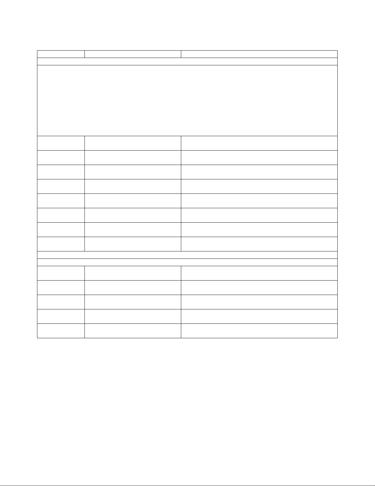
Table 6-3. Test Points (continued)
Test Point Signal Measurement and Conditions
A4A1/A4A3 LEFT TUNNEL BOARDS (FIGURE 6-6)
Leave meter or scope common connected to test point ((9)) when taking measurements at
test points 47 through 64. The measurements were taken with full-scale voltage and current
programmed. The measurements were made first in the CV mode with no load, and then in the CC mode
with the load set for full-scale voltage and current. Test points are listed for the first regulator (closest to fan)
and the last regulator stages only. The number of regulator stages that will be on (conducting) depends
upon the output current. In the CV mode with no load connected (no output current), only one or two stages
will be on conducting current through the down programmer stages. The remaining regulator stages will be
off (not conducting). In the CC mode with the load set for full-scale output voltage and current, all regulator
stages will be on.
TP47 U201-3 OUTPUT CONTROL
(comparator + input to all stages)
TP48 U201-2 Stage 1 comparator -input 0.05V in CV mode
TP49 U201-1 Stage 1 FET driver input 3.75V in CV mode
TP51 U202-2 Stage 3 comparator -input 0.05V in CV mode
TP52 U202-1 Stage 3 FET driver control -0.36V in CV mode
TP54 U202-5 DP CONTROL 0.22V in CV mode
TP55 U202-6 DP stage comparator -input 0.22V in CV mode
TP56 U202-7 DP stage comparator output -0.66V in CV mode
A4A2/A4A4 RIGHT TUNNEL BOARDS (FIGURE 6-7)
The same measurement conditions apply as described for the A4A1/A4A3 Left Tunnel Boards.
TP58 U301-3 OUTPUT CONTROL 47mV in CV mode
TP59 U301-2 Stage 1 comparator -input 47mV in CV mode
TP60 U301-1 Stage 1 FET driver control 3.3V in CV mode
TP62 U302-2 Stage 4 comparator -input 45mV in CV mode
TP63 U302-1 Stage 4 FET driver control -0.45V in CV mode
0.05V in CV mode
0.98V in CC mode
0.98V in CC mode
4.78V in CC mode
0.98V in CC mode
4.65V in CC mode
1.9V in CC mode
1.9V in CC mode
2.47V in CC mode
0.99V in CC mode
0.98V in CC mode
4.75V in CC mode
0.98V in CC mode
4.5V in CC mode
Service Addendum 45
Page 46

A1 Main Board Schematics (Figure 6-5)
The four schematic sheets for the A1 board included in this addendum replace
figures 6-2 and 6-5 in the standard Service Manual for the Agilent Series 665xA DC
Power Supplies.
The assembly drawing for the A1 main board included in this addendum replaces
Figure 6-5 in the standard Service Manual.
Left Tunnel Circuits (Figure 6-6)
The component locations and schematic drawings for the A4 left tunnel circuits
included in this addendum replace figure 6-6 in the standard Service Manual.
Right Tunnel Circuits (Figure 6-7)
The component locations and schematic drawings for the A4 right tunnel circuits
included in this addendum replace figure 6-7 in the standard Service Manual.
DSP Board (Figure 6-10)
The simplified component locations diagram for the A5 DSP board shows the
location of the troubleshooting test points on the J721 and J722 connectors
as well as the location of the two replaceable ROM chips, U734 and U735.
Because troubleshooting for the A5 DSP Board is to the assembly level only,
no schematics or parts lists are included for this board.
Adapter Board and Phone Adapter Board (Figures 6-11, 6-12)
The A6 Adapter board connects the A5 DSP board to the A1 main board.
The A7 Phone Adapter board connects the A5 DSP board to the A2 GPIB board.
Service Addendum46
Page 47

21
10
20
19
1
2
1
3
16
15
40
14
11
34
25
41
46
45
42
43
33
39
18
17
3
6
4
4
38
3
2
3
5
31
3
7
26
9
28
24
29
Figure 6-5. A1 Main Board Assembly Diagram and Test Points for E4350B
27
Page 48

Figure 6-5. A1 Main Board Schematic Diagram for E4350B (sheet 1 of 4)
Page 49

Figure 6-5. A1 Main Board Schematic Diagram for E4350B (sheet 2 of 4)
Page 50

Figure 6-5. A1 Main Board Schematic Diagram for E4350B (sheet 3 of 4)
Page 51

Figure 6-5. A1 Main Board Schematic Diagram for E4350B (sheet 4 of 4)
Page 52

Figure 6-6. A4 Left Tunnel Circuit Component Locations for E4350B
Figure 6-7. A4 Right Tunnel Circuit Component Locations for E4350B
Page 53

Figure 6-6. A4A1/A4A3 Left Tunnel Circuit Schematic Diagram for E4350B
Page 54

Figure 6-7. A4A2/A4A4 Right Tunnel Circuit Schematic Diagram for E4350B
Page 55

Figure 6-10. A5 DSP Board Test Points
Page 56

Figure 6-11. A6 Adapter Board Schematic Diagram
Page 57

Figure 6-12. A7 Phone Adapter Board Component Location and Schematic Diagram
 Loading...