

Page 1

User’s and Service Guide
Agilent Technologies 85024A
High Frequency Probe
Agilent Part Number 85024-90001
Printed in USA March 2000
Supersedes August 1989
Copyright © 1989–2000 Agilent Technologies, Inc. All rights reserved.
Page 2

Warranty
This product is warranted against defects in material and workmanship for a period of one
year from date of shipment. During the warranty period, Agilent Technologies will, at its
option, either repair or replace products which prove to be defective.
For warranty service or repair, this product must be returned to a service facility
designated by Agilent. Buyer shall prepay shipping charges to Agilent and Agilent shall
pay shipping chargestoreturn the product to Buyer. However, Buyer shall pay all shipping
charges, duties, and taxes for products returned to Agilent from another country.
Limitation of Warranty
The foregoing warranty shall not apply to defects resulting from improper or inadequate
maintenance by Buyer, Buyer-supplied software or interfacing, unauthorized modification
or misuse, operation outside of the environmental specifications for the product, or
improper site preparation or maintenance.
NO OTHER WARRANTY IS EXPRESSED OR IMPLIED. AGILENT TECHNOLOGIES
SPECIFICALLY DISCLAIMS THE IMPLIED WARRANTIES OF MERCHANTABILITY
AND FITNESS FOR A PARTICULAR PURPOSE.
Exclusive Remedies
THE REMEDIES PROVIDED HEREIN ARE BUYER’S SOLE AND EXCLUSIVE
REMEDIES. AGILENT TECHNOLOGIES SHALL NOT BE LIABLE FOR ANY DIRECT,
INDIRECT, SPECIAL, INCIDENTAL, OR CONSEQUENTIAL DAMAGES, WHETHER
BASED ON CONTRACT, TORT, OR ANY OTHER LEGAL THEORY.
Assistance
Product maintenance agreements and other customer assistance agreements are available
for Agilent products.
Forany assistance, contact the nearest Agilent sales or service office. Refer to Table 7-1 on
page 7-17 for a list of Aligent offices.
ii
Page 3
How to Use This Guide
SOFTKEY
This guide uses the following conventions:
Front Panel Key
CAUTION Caution denotes a hazard. It calls attention to a procedure that, if not
correctly performed or adhered to, would result in damage to or destruction of
the instrument. Do not proceed beyond a caution note until the indicated
conditions are fully understood and met.
WARNING Warning denotes a hazard. It calls attention to a procedure which, if
not correctly performed or adhered to, could result in injury or loss
of life. Do not proceed beyond a warning note until the indicated
conditions are fully understood and met.
NOTE All model numbers and part numbers published in this document are
HP/Agilent numbers, unless otherwise specified.
This represents a key physically located on the
instrument.
This represents a “softkey”, a key whose label is
determined by the instrument firmware.
iii
Page 4

Contents
1. General Information
Read This Before Using Your Probe . . . . . . . . . . . . . . . . . . . . . . . . . . . . . . . . . . . . . . . . . . . . .1-2
Input Voltage Tolerances . . . . . . . . . . . . . . . . . . . . . . . . . . . . . . . . . . . . . . . . . . . . . . . . . . . .1-2
Anti-Static Precautions . . . . . . . . . . . . . . . . . . . . . . . . . . . . . . . . . . . . . . . . . . . . . . . . . . . . . . .1-3
Product Description . . . . . . . . . . . . . . . . . . . . . . . . . . . . . . . . . . . . . . . . . . . . . . . . . . . . . . . . . .1-4
Specifications . . . . . . . . . . . . . . . . . . . . . . . . . . . . . . . . . . . . . . . . . . . . . . . . . . . . . . . . . . . . . . .1-5
General Characteristics. . . . . . . . . . . . . . . . . . . . . . . . . . . . . . . . . . . . . . . . . . . . . . . . . . . . . . .1-6
2. Accessories
Probe Features and Accessories. . . . . . . . . . . . . . . . . . . . . . . . . . . . . . . . . . . . . . . . . . . . . . . . .2-2
Probe Adapter. . . . . . . . . . . . . . . . . . . . . . . . . . . . . . . . . . . . . . . . . . . . . . . . . . . . . . . . . . . . . . .2-4
Description. . . . . . . . . . . . . . . . . . . . . . . . . . . . . . . . . . . . . . . . . . . . . . . . . . . . . . . . . . . . . . . .2-4
Operating Characteristics . . . . . . . . . . . . . . . . . . . . . . . . . . . . . . . . . . . . . . . . . . . . . . . . . . .2-4
Inspection . . . . . . . . . . . . . . . . . . . . . . . . . . . . . . . . . . . . . . . . . . . . . . . . . . . . . . . . . . . . . . . .2-4
10:1 Divider . . . . . . . . . . . . . . . . . . . . . . . . . . . . . . . . . . . . . . . . . . . . . . . . . . . . . . . . . . . . . . . .2-5
Operating Characteristics . . . . . . . . . . . . . . . . . . . . . . . . . . . . . . . . . . . . . . . . . . . . . . . . . . .2-5
Inspection . . . . . . . . . . . . . . . . . . . . . . . . . . . . . . . . . . . . . . . . . . . . . . . . . . . . . . . . . . . . . . . .2-5
Replaceable Parts . . . . . . . . . . . . . . . . . . . . . . . . . . . . . . . . . . . . . . . . . . . . . . . . . . . . . . . . . .2-6
Replacing the Probe Tip . . . . . . . . . . . . . . . . . . . . . . . . . . . . . . . . . . . . . . . . . . . . . . . . . . .2-6
3. Installation
Initial Inspection . . . . . . . . . . . . . . . . . . . . . . . . . . . . . . . . . . . . . . . . . . . . . . . . . . . . . . . . . . . .3-2
Certification . . . . . . . . . . . . . . . . . . . . . . . . . . . . . . . . . . . . . . . . . . . . . . . . . . . . . . . . . . . . . . . .3-2
Preparation for Use . . . . . . . . . . . . . . . . . . . . . . . . . . . . . . . . . . . . . . . . . . . . . . . . . . . . . . . . . .3-3
Power Requirements. . . . . . . . . . . . . . . . . . . . . . . . . . . . . . . . . . . . . . . . . . . . . . . . . . . . . . . .3-3
Mating Connectors. . . . . . . . . . . . . . . . . . . . . . . . . . . . . . . . . . . . . . . . . . . . . . . . . . . . . . . . . . .3-4
Returning the Product for Service. . . . . . . . . . . . . . . . . . . . . . . . . . . . . . . . . . . . . . . . . . . . . . .3-5
4. Operation
Operating Precautions. . . . . . . . . . . . . . . . . . . . . . . . . . . . . . . . . . . . . . . . . . . . . . . . . . . . . . . .4-2
Operating Instructions. . . . . . . . . . . . . . . . . . . . . . . . . . . . . . . . . . . . . . . . . . . . . . . . . . . . . . . .4-3
Grounding the Probe. . . . . . . . . . . . . . . . . . . . . . . . . . . . . . . . . . . . . . . . . . . . . . . . . . . . . . . .4-3
Retracting and Extending the Protective Sleeve. . . . . . . . . . . . . . . . . . . . . . . . . . . . . . . . . .4-3
Operator’s Check . . . . . . . . . . . . . . . . . . . . . . . . . . . . . . . . . . . . . . . . . . . . . . . . . . . . . . . . . . . .4-4
Operator’s check Using a Network Analyzer. . . . . . . . . . . . . . . . . . . . . . . . . . . . . . . . . . . . .4-4
Required Equipment . . . . . . . . . . . . . . . . . . . . . . . . . . . . . . . . . . . . . . . . . . . . . . . . . . . . . .4-4
Operator’s Check Using a Spectrum Analyzer . . . . . . . . . . . . . . . . . . . . . . . . . . . . . . . . . . .4-5
Required Equipment . . . . . . . . . . . . . . . . . . . . . . . . . . . . . . . . . . . . . . . . . . . . . . . . . . . . . .4-5
5. Performance Tests
Recommended Test Equipment. . . . . . . . . . . . . . . . . . . . . . . . . . . . . . . . . . . . . . . . . . . . . . . . .5-3
Network Analyzer Operation . . . . . . . . . . . . . . . . . . . . . . . . . . . . . . . . . . . . . . . . . . . . . . . . .5-4
Presetting the Network Analyzer. . . . . . . . . . . . . . . . . . . . . . . . . . . . . . . . . . . . . . . . . . . .5-4
Selecting a Transmission (or S21 Measurement) . . . . . . . . . . . . . . . . . . . . . . . . . . . . . . .5-4
Setting the Frequency Range . . . . . . . . . . . . . . . . . . . . . . . . . . . . . . . . . . . . . . . . . . . . . . .5-4
Setting CW Mode for Power Meter Measurements. . . . . . . . . . . . . . . . . . . . . . . . . . . . . .5-4
Setting the Output Power Level. . . . . . . . . . . . . . . . . . . . . . . . . . . . . . . . . . . . . . . . . . . . .5-4
Performing a Response Calibration . . . . . . . . . . . . . . . . . . . . . . . . . . . . . . . . . . . . . . . . . .5-4
Contents-v
Page 5

Contents
Median Gain and Frequency Response Flatness. . . . . . . . . . . . . . . . . . . . . . . . . . . . . . . . . . . 5-5
Description . . . . . . . . . . . . . . . . . . . . . . . . . . . . . . . . . . . . . . . . . . . . . . . . . . . . . . . . . . . . . . .5-5
Procedure . . . . . . . . . . . . . . . . . . . . . . . . . . . . . . . . . . . . . . . . . . . . . . . . . . . . . . . . . . . . . . . .5-5
Gain Compression . . . . . . . . . . . . . . . . . . . . . . . . . . . . . . . . . . . . . . . . . . . . . . . . . . . . . . . . . . . 5-6
Description . . . . . . . . . . . . . . . . . . . . . . . . . . . . . . . . . . . . . . . . . . . . . . . . . . . . . . . . . . . . . . .5-6
Procedure . . . . . . . . . . . . . . . . . . . . . . . . . . . . . . . . . . . . . . . . . . . . . . . . . . . . . . . . . . . . . . . .5-6
Calculating Equivalent Power. . . . . . . . . . . . . . . . . . . . . . . . . . . . . . . . . . . . . . . . . . . . . . . . 5-7
Average Noise Level . . . . . . . . . . . . . . . . . . . . . . . . . . . . . . . . . . . . . . . . . . . . . . . . . . . . . . . . .5-8
Description . . . . . . . . . . . . . . . . . . . . . . . . . . . . . . . . . . . . . . . . . . . . . . . . . . . . . . . . . . . . . . .5-8
Procedure . . . . . . . . . . . . . . . . . . . . . . . . . . . . . . . . . . . . . . . . . . . . . . . . . . . . . . . . . . . . . . . .5-8
Test Record. . . . . . . . . . . . . . . . . . . . . . . . . . . . . . . . . . . . . . . . . . . . . . . . . . . . . . . . . . . . . . . 5-9
6. Replaceable Parts
Introduction and Ordering Information. . . . . . . . . . . . . . . . . . . . . . . . . . . . . . . . . . . . . . . . . . 6-2
Parts Lists . . . . . . . . . . . . . . . . . . . . . . . . . . . . . . . . . . . . . . . . . . . . . . . . . . . . . . . . . . . . . . . . . 6-3
7. Service
Introduction . . . . . . . . . . . . . . . . . . . . . . . . . . . . . . . . . . . . . . . . . . . . . . . . . . . . . . . . . . . . . . . . 7-2
Before You Troubleshoot . . . . . . . . . . . . . . . . . . . . . . . . . . . . . . . . . . . . . . . . . . . . . . . . . . . . 7-2
Equipment Required for Troubleshooting. . . . . . . . . . . . . . . . . . . . . . . . . . . . . . . . . . . . . . . 7-2
Repair Strategy . . . . . . . . . . . . . . . . . . . . . . . . . . . . . . . . . . . . . . . . . . . . . . . . . . . . . . . . . . . . . 7-2
Probe Tip, Amplifier Microcircuit, and Regulator Assembly. . . . . . . . . . . . . . . . . . . . . . . .7-2
Main Cable and Plastic Sleeve Guide . . . . . . . . . . . . . . . . . . . . . . . . . . . . . . . . . . . . . . . . . . 7-2
Theory of Operation. . . . . . . . . . . . . . . . . . . . . . . . . . . . . . . . . . . . . . . . . . . . . . . . . . . . . . . . . . 7-3
ESD Protection at the Probe Tip. . . . . . . . . . . . . . . . . . . . . . . . . . . . . . . . . . . . . . . . . . . . . . 7-3
Troubleshooting Procedures. . . . . . . . . . . . . . . . . . . . . . . . . . . . . . . . . . . . . . . . . . . . . . . . . . . 7-4
Mechanical Failure of the Protective Sleeve. . . . . . . . . . . . . . . . . . . . . . . . . . . . . . . . . . . . . 7-4
Electrical Failure of the Probe. . . . . . . . . . . . . . . . . . . . . . . . . . . . . . . . . . . . . . . . . . . . . . . . 7-4
Visually Inspect the Probe Tip. . . . . . . . . . . . . . . . . . . . . . . . . . . . . . . . . . . . . . . . . . . . . .7-4
Power Supply Check. . . . . . . . . . . . . . . . . . . . . . . . . . . . . . . . . . . . . . . . . . . . . . . . . . . . . . 7-4
Replacement Procedure. . . . . . . . . . . . . . . . . . . . . . . . . . . . . . . . . . . . . . . . . . . . . . . . . . . . . . . 7-8
Replacing the Probe Tip. . . . . . . . . . . . . . . . . . . . . . . . . . . . . . . . . . . . . . . . . . . . . . . . . . . . . 7-8
Replacing the Amplifier Microcircuit . . . . . . . . . . . . . . . . . . . . . . . . . . . . . . . . . . . . . . . . . . 7-9
Removing the Plastic Regulator Housing Covers. . . . . . . . . . . . . . . . . . . . . . . . . . . . . . . . 7-10
Reassembling the Covers . . . . . . . . . . . . . . . . . . . . . . . . . . . . . . . . . . . . . . . . . . . . . . . . . 7-10
Replacing the Type-N Output Connector . . . . . . . . . . . . . . . . . . . . . . . . . . . . . . . . . . . . . . 7-11
Cable/Probe Wand Replacement . . . . . . . . . . . . . . . . . . . . . . . . . . . . . . . . . . . . . . . . . . . . . 7-12
Connector Inspection and Cleaning . . . . . . . . . . . . . . . . . . . . . . . . . . . . . . . . . . . . . . . . . . . . 7-15
Inspecting the Connectors . . . . . . . . . . . . . . . . . . . . . . . . . . . . . . . . . . . . . . . . . . . . . . . . . . 7-15
Visual Examination . . . . . . . . . . . . . . . . . . . . . . . . . . . . . . . . . . . . . . . . . . . . . . . . . . . . . . . 7-15
Cleaning Connectors . . . . . . . . . . . . . . . . . . . . . . . . . . . . . . . . . . . . . . . . . . . . . . . . . . . . . . 7-15
Contents-vi
Page 6

1 General Information
1-1
Page 7

General Information
Read This Before Using Your Probe
Read This Before Using Your Probe
Your probe has been designed to provide years of uninterrupted service. Excellent
performance at high frequencies requires the use of very small and delicate devices. Such
components can be damaged by careless use.
Input Voltage Tolerances
It is vital that the following specifications are not exceeded:
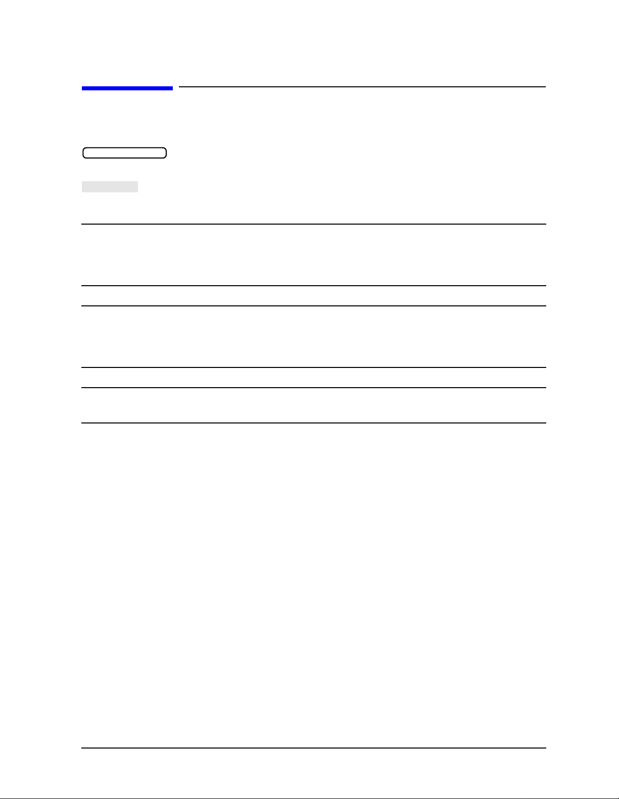
• Maximum safe DC input voltage (without 10:1 divider): ±50 V
• Maximum safe DC input voltage through a 10:1 divider: ±200 V
• Maximum safe RF voltage (without 10:1 divider): 1.5 V peak
• Maximum safe RF voltage through a 10:1 divider: 15 V peak
To minimize the potential for damage, always begin measurements with the 10:1 divider
attached. Remove the 10:1 divider only when both of the following conditions are met:
• RF and DC levels are known to within the above tolerances.
• Higher sensitivity is required than is possible with the 10:1 divider attached.
When the probe is stored, attach the 10:1 divider and place the anti-static protection cap
over the probe tip.
Figure 1 Probe with 10:1 Divider and Anti-Static Protection Cap
1-2 Chapter1
Page 8

General Information
Anti-Static Precautions
Anti-Static Precautions
Electrostatic discharge (ESD) is a serious problem; take consistent steps to eliminate it.
This is important whenever using your probe.
• Never touch the tip of the probe. The probe microcircuit is susceptible to damage by
static discharge.
• Eliminate ESD on the body. Wear a ground strap when using the probe.
• Eliminate ESD on the work surface. Use an anti-static bench mat. Never use the probe
near a workbench that is covered by carpet.
Do not introduce ESD into the device under test (DUT) while the probe is in use. If an
unprotected person touches part of the DUT, a static charge could damage the DUT as well
as the probe.
Chapter 1 1-3
Page 9

General Information
Product Description
Product Description
Your high frequency probe is an active probe that provides low input capacitance, high
input impedance, and wide bandwidth. The probe may be used with a variety of network
analyzers, spectrum analyzers, frequency counters, and oscilloscopes.
The probe allows the testing of high frequency RF circuits. High input impedance is
maintained by a Gallium Arsenide (GaAs) field effect transistor (FET) microcircuit.
When not in use, the probe tip is protected by a retractable grounded metal sleeve. This
helps prevent electrostatic discharge damage to the probe, and protects the tip from
breaking if the probe is dropped.
The probe tip may be inserted into the supplied probe adapter, adjusting the probe tip to a
50 Ω type-N male connector. The probe’s output connector is a type-N male.
1-4 Chapter1
Page 10

Specifications
Table 1-1 Product Performance
General Information
Specifications
Performance Parameter Value
Input Capacitance <0.7pF N
Input Resistance 1 MΩ N
Bandwidth 300 kHz to 3 GHz
(usable to 100 kHz)
Median Gain
(mid-point between max and min gains, 300 kHz to 1 GHz)
Frequency Response Flatness:
300 kHz to 1.0 GHz ±1.25 dB S
1.0 GHz to 3.0 GHz ±2.5 dB S
Average Noise Level:
10 MHz Bandwidth
3 GHz Bandwidth
Noise Figure:
<100 MHz <50 dB N
100 MHz to 3.0 GHz <25 dB N
c
0 dB ±1.25 dB S
<1 mV rms RTI
<17 mV rms RTI
d
(or −47 dBm)
d
(or −23 dBm)
Code
a, b
N
N
S
Gain Compression at 0.3 V Peak Input Voltage <1.0 dB S
Pulse Transition Time 200 ps N
Distortion at 0.3 V Peak Input Voltage
Maximum Safe RF Input Voltage:
Without 10:1 Divider 1.5 V peak S
With 10:1 Divider 15 V peak S
Maximum Safe DC Input Voltage:
Without 10:1 Divider ±50 V N
With 10:1 Divider ±200 V N
a. N = Nominal value: not warranted
S = Specification value: warranted
b. Specifications apply at 25 ˚C ±5 ˚C.
c. Relative to the Median Gain.
<
−30 dBc
d. Referred to Input
N
Chapter 1 1-5
Page 11

General Information
General Characteristics
General Characteristics
Physical Characteristics
Characteristics Value
Probe Length
Net Weight 0.3 kg (0.66 pounds)
Shipping Weight 2.3 kg (5.1 pounds)
a
130 cm (51 inches)
a. Overall length: includes wand, leads, and regulator assembly.
Environmental Characteristics
Environmental Requirements Operating Storage
Temperature
Altitude
Humidity Protect this product from temperature extremes which can cause
0 ˚C to +55 ˚C
Up to 4,600 meters (15,000 feet)
internal condensation.
−40 ˚C to +70 ˚C
Up to 15,000 meters (50,000 feet)
1-6 Chapter1
Page 12

2 Accessories
2-1
Page 13
Accessories
Probe Features and Accessories
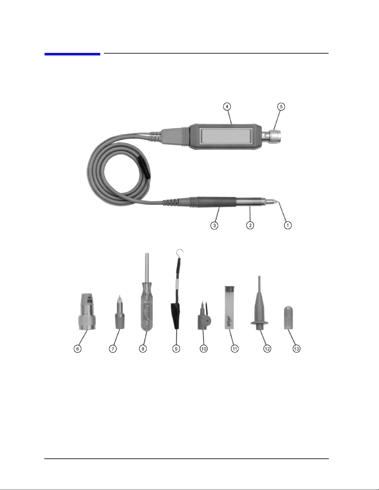
Probe Features and Accessories
Figure 2-1 Probe Features
2-2 Chapter2
Page 14

Table 2-1 Probe Features
Item Description Agilent
Part Number
1 Probe Tip 85024-60015
2 Protective Sleeve 85024-60014
3 Probe Wand 85024-60014
4 Regulator Assembly 85024-60001
5 RF Output connector (type-N male) 85024-60013
6 Probe tip to type-N adapter 11880-60001
7 10:1 divider 11881-60001
8 Probe tip nut driver 8710-1806
Accessories
Probe Features and Accessories
9 Ground lead, flexible 01123-61302
10 Slip-on tip with grounding spike 5060-0549
11 Replacement tip (short)
Replacement tip (long)
85024-60015
85024-60016
12 Hook tip adapter 10229A
13
Anti-static protection cap 08405-40003
Table 2-2 Available Accessories
Description Agilent Part or Model Number
Type-N Connector Gage Kit 85054B
a
Adapter, type-N female to Precision 7 mm
Adapter, type -N female to BNC male
b
External DC Power Supply 11899A
11524A
1250-1477
a. Used with the 85046A S-Parameter test set.
b. Used with the 8590A spectrum analyzer.
Chapter 2 2-3
Page 15

Accessories
Probe Adapter
Probe Adapter
Description
The probe adapter fits over the tip of the probe and converts the probe input to a 50 Ω
type-N male connector. The adapter is only used when performance testing the probe.
Operating Characteristics
Nominal Input Impedance 50 Ω
Frequency Range Same as the active probe (300 kHz to 3 GHz)
Inspection
Periodically inspect the threads of the adapter for signs of wear and damage. Inspect the
barrel of the probe receptacle, making sure it is clean and free of grit. Clean the adapter
threads or receptacle with clean compressed air.
2-4 Chapter2
Page 16

Accessories
10:1 Divider
10:1 Divider
The 10:1 divider fits over the tip of the probe and provides the following changes to the
probe’s operating parameters:
• Increases (by a factor of 10) the input voltage at which 1 dB compression occurs.
• Decreases the input capacitance without changing input resistance, thereby decreasing
capacitive loading.
Two or more dividers may be cascaded to provide higher divide ratios.
Operating Characteristics
Divider Ratio 10:1
Input Capacitance Typically <0.7 pF
Input Resistance 1 MΩ
Input Voltage for 1 dB Compression
Maximum Safe DC Input Voltage
Maximum Safe RF Input Voltage 15 Volts Peak
Frequency Range Same as the active probe (300 kHz to 3 GHz)
a. When used with the active probe.
3.0 Volts Peak
±200 Volts
a
a
Inspection
Make sure the tip is not bent or discolored. Periodically inspect the barrel of the probe
receptacle, making sure it is clean and free of grit. Clean the receptacle with clean
compressed air.
When cascading 10:1 dividers, periodically inspect and clean the exterior of the metal
sleeve.
Chapter 2 2-5
Page 17

Accessories
10:1 Divider
Replaceable Parts
If the tip is discolored, bent or broken, it must be replaced. Follow the procedure outlined
in “Replacing the Probe Tip,” below.
Figure 2-2 Exploded View of 10:1 Divider
Item Description Part Number
1 Short probe tip 85024-60015
Long probe tip 85024-60016
2 Guide 11881-20007
Replacing the Probe Tip
1. Remove the 10:1 divider from the probe.
2. Unscrew the damaged tip with a 3/32 nut driver supplied with the probe and discard
the tip.
3. Screw on the new tip and lightly tighten it with a 3/32 inch nut driver.
(Overtightening the tip can damage the nose assembly.)
2-6 Chapter2
Page 18

3 Installation
3-1
Page 19

Installation
Initial Inspection
Initial Inspection
If the shipping container or cushioning material is damaged, keep it until the contents of
the shipment are checked for completeness, and the product is checked both mechanically
and electrically. Procedures for checking the electrical performance are given in
Chapter 5 , “Performance Tests.”
Notify the nearest Agilent Technologies office if the product does not pass performance
tests, the shipping contents are incomplete, or if there is mechanical damage or defect.
Notify the carrier if the shipping container is damaged or if the cushioning material shows
signs of stress. Keep all shipping materials for the carrier’s inspection. Agilent
Technologies will arrange for repair or replacement without waiting for a claim settlement.
Certification
Agilent Technologiescertifies that this product met its published specifications at the time
of shipment from the factory. Agilent further certifies that its calibration measurements
are traceable to the United States National Institute of Standards and Technology (NIST,
formerly NBC), to the extent allowed by the institute’s calibration facility, and to the
calibration facilities of other International Standards Organization members.
3-2 Chapter3
Page 20

Installation
Preparation for Use
Preparation for Use
CAUTION Electrostatic discharge (ESD), excessive input signals or mechanical shock
can dramatically degrade the performance of the probe. Be sure to observe
the following precautions.
• Never touch the tip of the probe!
• Always hold the probe by the retracted metal sleeve.
• Work at a workstation equipped with an anti-static mat.
• Extend the protective sleeve when not actually taking measurements.
• Wear an anti-static wrist strap and avoid introducing static electricity into the device
under test (DUT) or test setup.
• Make sure the device under test (DUT) is at the same ground potential as the probe.
Power Requirements
If using the probe with an instrument that does not supply probe power, use a separate
power supply (such as the 11899A DC power supply) which provides two probe power
connections. Make sure that any separate supply used meets the requirements shown in
Table 3-1. A male power connector is available for use with the probe (part number
5060-0467).
Table 3-1 Probe Power Supply Requirements and Connector Pin-outs
Pin Voltage Current
1 −12.6 V ±20% 75 mA
2 GND
3 +15 V ±20% 150 mA
a. As seen looking into the probe’s power connector.
a
Chapter 3 3-3
Page 21

Installation
Mating Connectors
Mating Connectors
CAUTION Periodically inspect and, if necessary, clean the type-N output connector.
Refer to Chapter 7, “Connector Inspection and Cleaning,” on page 15. The
probe adapter should be inspected at the same time, and cleaned if necessary.
3-4 Chapter3
Page 22

Installation
Returning the Product for Service
Returning the Product for Service
Contact Agilent Technologies before returning the probe for service. See Table 7-1 on
page 7-17. When shipping the probe to Agilent Technologies please include a blue service
tag (found at the end of this manual) and a valid return mailing address. Products cannot
be returned to a post office box. Provide the name and phone number of a contact person
within your organization, the complete model and serial number of the product, and a
complete description of the problem.
When shipping the probe for any reason, be sure to use the original (or comparable)
packaging materials. Also mark the container FRAGILE to assure careful handling of the
device.
When making inquiries, either by correspondence or by telephone, please refer to the probe
by model and full serial number. Refer to Table 7-1 on page 7-17 for a list of Agilent
Technologies sales and service offices.
Chapter 3 3-5
Page 23

4 Operation
4-1
Page 24

Operation
Operating Precautions
Operating Precautions
CAUTION Electrostatic discharge (ESD), excessive input signals or mechanical shock
can dramatically degrade the performance of the probe. Be sure to observe
the following precautions.
• Never touch the tip of the probe!
• Always hold the probe by the retracted metal sleeve.
• Work at a workstation equipped with an anti-static mat.
• Extend the protective sleeve when not actually taking measurements.
• Wear an anti-static wrist strap and avoid introducing static electricity into the device
under test (DUT) or test setup.
• Make sure the device under test (DUT) is at the same ground potential as the probe.
4-2 Chapter4
Page 25

Operation
Operating Instructions
Operating Instructions
CAUTION Discharging the Probe Between Measurements
Measuring a node having a DC voltage potential charges blocking capacitors
inside of the probe. Ground the probe tip after measuring such nodes to
discharge the probe capacitors. Failure to do this can result in damage to
sensitive circuits in the DUT, especially if it is an active device.
Grounding the Probe
Proper grounding is important when making measurements with any probe. The probe is
supplied with two grounding devices: an alligator-type ground clip and a slip-on type
ground tip. Use the shortest ground path possible. Proper grounding becomes more
important as frequency increases. For optimum measurements in a factory environment,
design your circuits with ground-plane feedthroughs next to every test point.
Retracting and Extending the Protective Sleeve
Hold the probe wand in one hand, pointing the tip away from yourself. Grasp the probe
sleeve in the other hand and turn about 1/4 turn counter-clockwise. Now, pull the sleeve
toward you while slowly turning it counter-clockwise. The sleeve will now retract quickly
with little counter-clockwise rotation. Reverse this procedure to extend the sleeve.
Chapter 4 4-3
Page 26

Operation
Operator’s Check
Operator’s Check
The operator’s check is designed to be a simple functional test for the probe. If the probe
fails the operator’s check, or if you need to verify that the probe meets its warranted
specifications, you will need to do the performance tests as described in Chapter 5 ,
“Performance Tests.”
The operator’s check can be performed with either a network analyzer or a spectrum
analyzer. Use one of the following two procedures to perform the operator’s check.
Operator’s check Using a Network Analyzer
Required Equipment
Item Part Number
Network Analyzer Any compatible with
type-N connectors
Type-N Cable 50Ω, male connectors
Probe Adapter 11880-60001
Procedure
NOTE If you are not familiar with network analyzer operation, refer to “Network
Analyzer Operation” on page 5-4 for basic information about performing the
analyzer operations used in this procedure.
1. Preset the analyzer using the hardkey.
PRESET
2. Configure the analyzer to measure transmission.
3. Set the output power level of the analyzer to 0 dBm.
4. Set the frequency sweep range on the analyzer from 300 kHz to 3 GHz.
5. Connect a type-N cable (a through cable) between the output and the input ports on the
analyzer.
6. Perform a response calibration on the analyzer. The trace on the analyzer should now
be flat at 0 dB.
7. Remove the through cable. Connect the probe adapter to the output port of the analyzer.
Connect the output of the probe to the input port of the analyzer. Connect the probe
power cable to a power source.
8. Plug the probe tip into the adapter.
9. The trace of the analyzer should be within ± 5 dB of 0 dB.
4-4 Chapter4
Page 27

Operation
Operator’s Check
Operator’s Check Using a Spectrum Analyzer
Required Equipment
Item Part Number
Spectrum Analyzer Any Compatible
Adapters As Necessary
Probe Adapters 11880-60001
Procedure
1. Connect the spectrum analyzer’s calibration output directly to its RF input. Turn on the
spectrum analyzer.
2. Set the spectrum analyzer center frequency to the frequency of the calibration output.
3. Set the frequency span to 10 MHz and activate a marker.
4. Place the marker on the peak of the displayed signal and note the value in dBm.
5. Connect the probe adapter to the calibration output.
6. Connect the probe output to the RF input on the analyzer.
7. Connect the probe power cable to a power source.
8. Plug the probe tip into the probe adaptor.
9. Place the marker on the peak of the displayed signal and compare the signal level in
dBm to that measured in step 4. The probe should not cause more than 5 dBm of signal
loss.
Chapter 4 4-5
Page 28

5 Performance Tests
5-1
Page 29

Performance Tests
The procedures in this chapter test the probe to ensure that it meets the warranted
specifications listed in Table 1-1 on page 1-5. The “Test Record” on page 5-9 provides space
to record the test results. Each of the tests can be performed without access to the interior
of the probe. Follow the procedures, record data on the “Test Record” on page 5-9, perform
the calculations, and determine pass or fail for each test item. All tests must pass for the
performance test to be verified.
NOTE The performance tests in this chapter cover the specifications for a standard
85024A probe. If the serial number label indicates an option, contact Agilent
Technologies for applicable specifications. Refer to Table 7-1 on page 7-17 for
a list of Agilent Technologies sales and service offices.
5-2 Chapter5
Page 30

Performance Tests
Recommended Test Equipment
Recommended Test Equipment
Table 5-1 lists the equipment that is recommended for use in performance testing of the
probe. Other equipment may be substituted if its specifications meet or exceed the
specifications listed in the “Critical Specifications” column.
Table 5-1 Recommended Test Equipment
Type Critical Specifications Recommended Model or Part
Number
Vector Network Analyzer 300 kHz to 3 GHz
Power Meter 437B/438A, or E4418A/E4419A
Power Sensor 300 kHz to 3 GHz
−30 dBm to +5 dBm
Type-N Cable, male-to-male 50Ω 8120-8862 or equivalent
Probe Adapter Supplied with probe 11880-60001
Attenuator, type-N, 50 Ω any value 10 to 20 dB
nominal
Type-N Adapter, female-to-female 1250-0777 or equivalent
a. Many models of network analyzers can be used for these performance tests. The network
analyzer must cover the frequency range 300 kHz to 3 GHz, and be capable of power
output in the range of −3 to +5 dBm.
8714ET/ES, 8753ET/ES, 8753E
8482A
8491A/B/C Option 20, Option 10,
or equivalent
a
Chapter 5 5-3
Page 31

Performance Tests
Transmission
Fwd Trans S21
Transmission
TRANS:FWD
CW
Hold
Continuous
CW FREQ
TRIGGER MENU
HOLD
CONTINUOUS
SWEEP TYPE MENU
LIN FREQ
Power
Response
Measure Standard
User Response
Response
Measure Standard
CALIBRATE MENU
Response
THRU
Recommended Test Equipment
Network Analyzer Operation
This section provides some general information for performing basic network analyzer
operations. For more specific operating information, refer to your analyzers user’s guide.
Presetting the Network Analyzer
All analyzers have a hardkey for this function.
PRESET
Selecting a Transmission (or S21 Measurement)
871x family
8753 family
Press , then or .
Press or , then followed by or
MEAS 1
Chan 1 CH 1 Meas
.
Setting the Frequency Range
871x family
8753 family
Start and stop frequencies are accessed via .
Start and stop frequencies are accessed via and .
Setting CW Mode for Power Meter Measurements
871x family
8753 family
Press , then and set the Trigger mode to . To
return to normal operation, set the trigger mode to and define
start and stop frequencies.
Press or to access both the sweep and trigger
FREQ
Menu Sweep Setup
MENU
functions. The softkey activates CW mode, press
then . To return to normal operation,
change the trigger mode to , or
Sweep Setup
, then followed by .
FREQ
Start Stop
Menu
Setting the Output Power Level
871x family
8753 family
Performing a Response Calibration
871xC and 871xET
871xES
8753 family
5-4 Chapter5
Press .
Press or to access .
POWER
Menu Sweep Setup
Press , then .
CAL
Press when the through cable is connected.
Press , , then .
CAL
Press when the through cable is connected.
Press , , then .
Cal
Press when the through cable is connected.
Page 32

Performance Tests
Median Gain and Frequency Response Flatness
Median Gain and Frequency Response Flatness
Specifications (at 25 ˚C ±5 ˚C)
Median Gain over 300 kHz to 1 GHz 0 dB ±1.25 dB
Frequency Response Flatness (Relative to Median Gain)
300 kHz to 1 GHz ±1.25 dB
1 GHz to 3 GHz ±2.5 dB
Description
This test procedure performs a response calibration on the analyzer and then measures
the gain of the probe over frequency. Maximum and minimum gains in two different
frequency bands are used to determine the probe performance.
Procedure
1. Preset the analyzer using the hardkey.
2. Set the frequency sweep range for 300 kHz to 3 GHz.
3. Set the analyzer for a transmission (S21) measurement.
4. Connect a type-N cable between the output port and input port on the analyzer.
5. Perform a response calibration on the analyzer. The trace on the analyzer should now
be a flat line at 0 dB.
6. Disconnect the cable from the output port of the analyzer. Connect the type-N barrel to
the free end of the cable.
7. Connect the probe adapter to the output port of the analyzer. Connect the probe
between the probe adapter and the type-N barrel. Plug the probe power cable into the
front panel of the analyzer.
8. Read the following four values from the trace on the analyzer and enter the values on
the “Test Record” on page 5-9. Use the network analyzer marker functions as needed.
Maximum gain in dB over the frequency range of 300 kHz to 1 GHz (A).
Minimum gain in dB over the frequency range of 300 kHz to 1 GHz (B).
Maximum gain in dB over the frequency range of 1 GHz to 3 GHz (C).
PRESET
Minimum gain in dB over the frequency range of 1 GHz to 3 GHz (D).
Perform the calculations indicated on the test record to determine the results of the
test.
Chapter 5 5-5
Page 33

Performance Tests
Gain Compression
Gain Compression
Specifications (at 25 ˚C ±5 ˚C) <1.0 dB at 0.3 V Peak
In a 50 Ω system 0.3 V Peak = −0.458 dBm
Description
This test identifies the frequency of greatest compression at a signal level of 0.3 V peak
(
−0.458 dBm). It then uses a power meter to precisely measure the compression at that
frequency.
Procedure
1. Select an attenuator to use: its nominal value must be in the 10 to 20 dB range.
2. Plug the power sensor into the power meter and turn on the power meter. Allow them to
warm up for 3 minutes.
3. Calibrate and zero the power meter and the power sensor.
4. Preset the analyzer using the hardkey.
5. Set up the analyzer to measure transmission (S21) over the 300 kHz to 3 GHz range.
6. Set the power level on the analyzer to 0 dBm.
7. Connect the probe adapter to the output of the analyzer.
8. Connect the output of the probe to the input port of the analyzer.Plug the probe tip into
the adapter. Connect the probe power cable to a power source.
9. Perform a response calibration on the analyzer using the probe as the “through cable.”
The trace on the analyzer should now be a flat line at 0 dB.
10.Insert the attenuator between the output port of the analyzer and the probe adapter.
Reconnect the probe to the probe adapter.
11.Determine the frequency of peak gain on the trace of the analyzer. Record the frequency
on the test record.
12.Set the analyzer to CW mode for power meter measurements. Set the CW frequency to
the value determined in the previous step.
13.Remove the attenuator from the output port of the analyzer.
14.Connect the power sensor to the output port of the analyzer. Adjust the analyzer power
output level to produce a reading of 0.0 dBm on the power meter.(Note: 0.0 dBm is used
to allow for possible inaccuracy of power meters).
PRESET
15.Disconnect the power sensor from the output port of the analyzer. Connect the
attenuator to the output port of the analyzer.
5-6 Chapter5
Page 34

Performance Tests
Gain Compression
16.Connect the probe, the probe adapter, and a barrel between the attenuator and the
power sensor. The signal from the analyzer should now go through the attenuator and
then the probe before reaching the power sensor. Record the power reading on the “Test
Record” on page 5-9 (item F).
17.Remove the attenuator pad, connect the probe adapter to the output port of the
analyzer. Connect the attenuator pad between the probe and the power sensor. The
signal from the analyzer should now go through the probe and then the pad before
reaching the power sensor. Record the power reading on the “Test Record” on page 5-9
(item G).
18.Perform the calculation indicated on the test record to determine the result of the test.
Calculating Equivalent Power
The probe is usually used as a high impedance device. The compression specification is
given as a voltage (instead of power) because of the wide range of devices with which the
probe may be used. For testing the probe, the probe adapter is used to make the probe
input 50 Ω. Using this known impedance, an equivalent power can be calculated.
To find the power level equivalent to the 0.3 peak voltage, perform the following
mathematical steps:
Steps Formula Example
1. Convert the peak voltage into RMS.
2. Convert the RMS voltage to a raw power.
3. Convert the raw power to a power
which is relative to 1 mW.
4. Convert to dBm.
V
pk
-------------------------
1.4142135
2
V
------
R
divide by 0.001w
10 LOGx()
0.3V
------------------------- 0.212132V
1.4142135
0.212132
--------------------------- 0.0009w=
50Ω
0.009w
----------------- 0.9=
0.001w
10 LOG 0.9()0.458 dBm
=
2
)
–=
* Therefore, as shown in the example, the equivalent power to 0.3 V peak in a 50 Ω
system is −0.458 dBm.
RMS
*
Chapter 5 5-7
Page 35

Performance Tests
Average Noise Level
Average Noise Level
Specifications (at 25 ˚C ±5 ˚C): <17 mV RTI (or −23 dBm at probe output)
Description
This test procedure uses a power meter to measure the power level of the probe output
when the probe tip is connected through 50 ohms to ground.
Procedure
1. Connect the power sensor to the power meter and allow the power meter to warm up for
five minutes.
2. Calibrate and zero the power meter.
3. Enable averaging on the power meter.
4. Connect the power cable on the RF probe to a power source, allow the probe to warm up
for at least three minutes.
5. Connect the probe tip adapter to the tip of the probe. (This effectively grounds the probe
tip).
6. Connect the RF probe to the power sensor using a type-N barrel.
7. Read the power meter. If the reading is unstable, visually determine the approximate
peak value over a period of about twenty seconds. Record that value on the test record.
5-8 Chapter5
Page 36
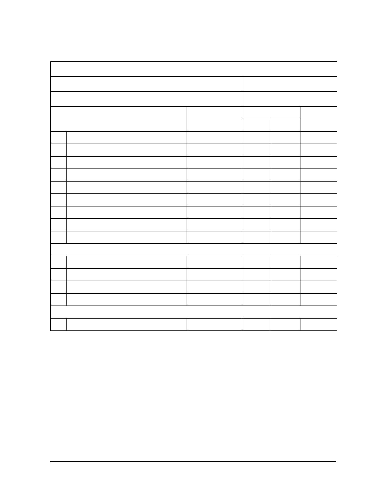
Test Record
85024A High Frequency Probe Test Record
Serial Number: Date:
Tested By: Temperature:
Performance Tests
Average Noise Level
Median Gain and Frequency Response
Results
a
Limits
Flatness
A Maximum gain over 300 kHz to 1 GHz
B Minimum gain over 300 kHz to 1 GHz
C Maximum gain over 1 GHz to 3 GHz
D Minimum gain over 1 GHz to 3 GHz
E Median Gain (A+B)/2 =
LF maximum gain A − E=
LF minimum gain B −Ε=
HF maximum gain C − E=
HF minimum gain D −Ε=
dB
dB
dB
dB
dB
dB
dB
dB
dB
N/A N/A N/A
N/A N/A N/A
N/A N/A N/A
N/A N/A N/A
1.25 −1.25
1.25 0
0 −1.25
2.5 −2.5
2.5 −2.5
Gain Compression
Frequency at maximum gain N/A N/A N/A
F Pad before probe
G Pad after probe
dBm
dBm
N/A N/A N/A
N/A N/A N/A
Pass/
FailMax Min
Compression, F − G=
dBm
+1.0 Ν/Α
Average Noise Level
Power level
dBm
−23 N/A
a. Reminder: Include polarity (+/−) in all recorded values and calculations.
Chapter 5 5-9
Page 37

6 Replaceable Parts
6-1
Page 38

Replaceable Parts
Introduction and Ordering Information
Introduction and Ordering Information
The replaceable parts lists are organized as follows:
• Table 6-2 contains components and assemblies of the high frequency probe given in
alphabetic/numerical order by reference designation.
• Table 6-3 contains components of the A1 regulator assembly listed in
alphabetic/numerical order by reference designation.
NOTE The total quantity for each part is given only once, at the first appearance of
the part in the list.
To order a part listed in the replaceable parts list, indicate the Agilent part number and
the quantity desired. Address the order to the nearest Agilent Technologies office.
To order a part that is not listed in the replaceable parts list, include the probe model and
serial number, the description and function of the part and the quantity desired. Address
the order to the nearest Agilent Technologies office. See page 7-17 for a list of Agilent
Technologies sales and service offices.
6-2 Chapter6
Page 39

Parts Lists
Table 6-1 Miscellaneous Replacement Parts
Part Number Qty Description
Replaceable Parts
Parts Lists
08405-40003 1
1401-0214 1 Protective End Cap for type-N Connector
85024-90001 1 Operating and Service manual
85024-80001 2 Side Label
85024-80003 1 Product Case
85024-80004 1 Bottom Foam of the Product Case
5180-8448 1 Top Foam of the Product Case
01123-61302 1
5060-0549 1
10229A 1
8710-1806 1
11880-60001 1
11881-60001 1
Service Tool
85024-20041
Anti-Static Protection Cap
Ground Lead, Flexible
Ground Tip, Slip-On with Grounding Spike
Hook Tip Adapter
3/32 inch Probe Tip Nut Driver
Type-N Probe Adapter
10:1 Divider
Spanner / Wrench (see Figure 7-10
a
a
a
a
a
a
)
a
General Accessories
1250-1477
a. Shown in Figure 2-1.
b. For use with the 8590A Spectrum Analyzer.
Adapter, type-N female to BNC male
b
Chapter 6 6-3
Page 40

Replaceable Parts
Parts Lists
Table 6-2 Replaceable Parts
a
Item
1 85024-60013 Connector Replacement Kit
2 85024-20024 1 RF Bead
3 85024-20016 1 Transition-Nut
4 85024-20017 1 Transition-REG
5 0515-0912 2 Screw-Machined M3 x 0.5 8 mm-LG Pan Head
6 85024-20028 1 Frame Casting
7 85024-20025 1 Nut, Strain Relief
8 85024-60014 Cable/Probe Wand Kit (pre-assembled)
9 0515-0950 2 Screw-Machined M2 8 mm-LG Pan Head
10 0515-0976 2 Screw-Machined M2 6 mm-LG Pan Head
11 85024-20015 1 Probe Nut
12 85024-60015 1 Short Power Tip (also used on 10:1 Divider)
13 85024-60011 1 Nose Assembly
Part Number Qty Description
85024-60016 1 Long Power Tip
14 85024-40007 1 Conductive Washer
15 85024-60005 1 Amplifier Microcircuit
16 85024-20037 1 Clip Spring for Elastic Conductive Strip
17 85024-20035 1 Elastic Conductive Strip
18 85024-40001 1 Regulator assembly Plastic Covers (set)
19 85024-00002 1 Housing Reinforcement
20 5040-0494 1 Connector Sleeve (power)
21 5060-0466 1 Connector Body (power)
a. See Figure 6-1, “Replaceable Parts Identification.”
6-4 Chapter6
Page 41

Figure 6-1 Replaceable Parts Identification
Replaceable Parts
Parts Lists
* CAUTION Failure to remove the nose assembly prior to replacing the tip will result in
damage to the conductive elastometer on the tip assembly.
** NOTE Item 11 is a nut which slides over items 12 through 17 and screws onto the
end of the heat sink.
Chapter 6 6-5
Page 42

Replaceable Parts
Parts Lists
Table 6-3 A1 Regulator Assembly Replaceable Parts
Reference
Designation
A1 85024-60014 1 Regulator Assembly
A1C1 0160-3879 2 Capacitor-FXD 0.01µF ±20% 100VDC CER
A1C2 0180-3771 6 Capacitor-FXD 1µF ±10% 35VDC Ta
A1C3 0180-3771 Capacitor-FXD 1µF±10% 35VDC Ta
A1C4 0180-3771 Capacitor-FXD 1µF±10% 35VDC Ta
A1C5 0160-3879 Capacitor-FXD 0.01µF±20% 100VDC CER
A1C6 0180-3771 Capacitor-FXD 1µF±10% 35VDC Ta
A1C7 0180-3771 Capacitor-FXD 1µF±10% 35VDC Ta
A1C8 0180-3771 Capacitor-FXD 1µF±10% 35VDC Ta
A1MP1 Not Assigned
A1MP2 1200-0172 1 Insulator-Transistor DAP-GL
A1MP3 85024-20033 1 Heatsink-REG
A1MP4 0340-0949 2 Insulator-Transistor Thermal Conductor
A1MP5 3050-1021 2 Washer, Shoulder No. 4 0.116-in.-ID 0.215-in.-OD
Part Number Qty Description
a
A1MP6 0515-0912 2 Screw-Machine M3 x 0.5 8 mm-LG Pan Head
A1MP7 0361-0010 2 Rivet-AL 0.123D x 0.219L
A1Q1 1854-0477 1 Transistor NPN 2N2222A SI TO-18 PD = 500 MW
A1R1 0698-3391 1 Resistor 21.5 1% 0.5 W FTC = 0±100
A1R2 0757-0442 1 Resistor 10k 1% 0.125 W FTC = 0±100
A1R3 0698-0083 1 Resistor 1.96k 1% 0.125 W FTC = 0±100
A1R4 0757-0416 1 Resistor 511 1% 0.125 W FTC = 0±100
A1R5 0698-3437 2 Resistor 133 1% 0.125 W FTC = 0±100
A1R6 0757-0198 1 Resistor 100 1% 0.5 W FTC = 0±100
A1R7 0698-3444 1 Resistor 316 1% 0.125 W FTC = 0±100
A1R8 0698-3437 Resistor 133 1% 0.125 W FTC = 0±100
A1U1 1826-0393 1 IC V Regulator-Adjust-Pos 1.2 / 37 V TO-220 pkg.
A1U2 1826-0527 1 IC 337 V Regulator-Adjust-Neg TO-220 pkg.
a. If necessary, refer to “A1 Regulator Assembly Component Locations Diagram” on page 7-7.
6-6 Chapter6
Page 43

7 Service
7-1
Page 44

Service
Introduction
Introduction
This chapter contains troubleshooting and repair information. Heed caution signs to avoid
damaging the probe. You may wish to read the “Theory of Operation” on page 7-3, with its
associated diagrams as an aid to troubleshooting.
Before You Troubleshoot
Troubleshooting the probe begins with performing the “Operator’s Check” on page 4-4, and
the Chapter 5 , “Performance Tests.” If the probe does not pass the performance tests, refer
to the “Troubleshooting Procedures” on page 7-4.
Equipment Required for Troubleshooting
Troubleshooting procedures require the use of a digital multimeter.
Repair Strategy
Probe Tip, Amplifier Microcircuit, and Regulator Assembly
The probe tip and amplifier microcircuit are easily replaced. The regulator assembly (A1)
repair can be performed at either assembly or component level. Module exchange
programs are not available for this product.
Main Cable and Plastic Sleeve Guide
The main cable includes the probe wand, the main cable and the smaller power supply
cable. If the cable is damaged, both the cable and the probe wand assembly must be
replaced as a single unit. In this case, take the following parts off of the old probe for use
on the replacement probe:
• The nose assembly
• Nut
• Amplifier microcircuit
These items are shown in Figure 7-6 on page 7-8 and Figure 7-7 on page 7-9.
A kit is available that provides a preassembled main cable and probe wand. The wand does
not come with the amplifier microcircuit, nose-assembly, or tip, because these may be
easily removed from your old probe wand. Refer to Table 6-2 on page 6-4, for the part
number of the kit.
7-2 Chapter7
Page 45

Service
Theory of Operation
Theory of Operation
The probe uses a Gallium Arsenide FET integrated circuit amplifier which provides unity
gain. This amplifier microcircuit requires +6 V and −4 Vdc to operate. These voltages are
provided by the regulator assembly.
The regulator assembly converts the +15 volt and −12.6 volt supplies from the host
instrument with two voltage regulators. The regulator supplies the +6 and −4 voltages to
the amplifier microcircuit.
The most common failures in the probe will all result in loss of signal through the probe,
and will show up if the operator’s check is performed. The most common failures are
expected to be:
1. Destruction of the amplifier microcircuit due to static electricity (proper anti-static
precautions not taken).
2. Probe power tip damage (caused by the operator dropping the probe with the sleeve
retracted).
3. Possible regulator failure.
ESD Protection at the Probe Tip
The FET integrated circuit amplifier is located at the tip of the probe. The FET input of the
amplifier is protected by a bidirectional voltage limiter as shown in Figure 7-1.
Figure 7-1 Probe Tip Input Circuit
The voltage limiter element has a negligible effect on circuit operation for input voltages
within specification. The voltage limiter is a non-linear element: it begins to conduct
current at about 2.5 volts. It effectively limits voltages at the amplifier input to less than
± 4 volts. This prevents amplifier damage from low levels of ESD.
Even with the protection provided by the voltage limiter element, the probe is still
sensitive to ESD. High levels of ESD can cause permanent damage to the voltage limiter
element itself. Careful ESD precautions must be observed when using the probe.
Chapter 7 7-3
Page 46

Service
Troubleshooting Procedures
Troubleshooting Procedures
CAUTION The probe contains an input GaAs amplifier microcircuit that is highly
sensitive to electrostatic discharge (ESD). When repairing this probe, you
must use an anti-static wrist strap, and work at a station equipped with an
anti-static surface! Before you take a measurement with a digital multimeter,
discharge the leads by touching them to ground.
Mechanical Failure of the Protective Sleeve
The probe wand/cable must be replaced if the protective sleeve fails to slide and lock
properly.
Electrical Failure of the Probe
Visually Inspect the Probe Tip
Inspect the probe tip for damage. If it is bent or broken, replace it by referring to
“Replacing the Probe Tip” on page 7-8. Perform the “Operator’s Check” on page 4-4. If the
problem persists, perform the following procedure.
Power Supply Check
Refer to the probe schematic in Figure 7-2 on page 7-5 when performing the following
procedure.
1. Check the probe power output from the supplying instrument or power supply. The
output pins and voltages are shown in Figure 7-4 on page 7-6. Check continuity of the
ground pin to chassis ground; it should be less than 1Ω.
• If the supplies are within the tolerances given in Table 3-1 on page 3-3, continue to
step 2.
• If the voltage is not present at the supplying device, or the ground pin is open,
troubleshoot as required. Suspect a broken wire going to the probe power jack.
2. Follow the procedure in “Replacing the Amplifier Microcircuit” on page 7-9, to remove
the probe’s nose assembly, amplifier microcircuit, elastic conductive strip, and spring
clip. These items are illustrated in Figure 7-3 on page 7-5.
7-4 Chapter7
Page 47

Troubleshooting Procedures
Figure 7-2 A1 Regulator Schematic Diagram and Overall Block Diagram
Service
Figure 7-3 High Frequency Probe
Chapter 7 7-5
Page 48

Service
Troubleshooting Procedures
3. Connect the probe’s power cord to the power source. Turn the power source on.
4. Refer to Figure 7-4. Check the +6 V and −4 V power supply voltages on the exposed
portion of the probe end.
• If the voltages are good, suspect an amplifier microcircuit failure. Replace the
amplifier microcircuit and do not perform the following steps.
5. If one of these voltages is bad, follow the procedure in “Removing the Plastic Regulator
Housing Covers” on page 7-10, and continue with the following steps.
6. Refer to Figure 7-4. Disconnect the power supply cable and check the continuity of the
three input lines to the A1 regulator assembly. If one of the wires is broken internally,
replace the cable/probe wand assembly.
7. If the three input lines show continuity, desolder the −4 V and +6 V output wires shown
in Figure 7-4. Measure the +6 V and −4 V feed throughs on the printed circuit board. If
the voltages are good replace the cable/probe wand assembly. If one of the voltages is
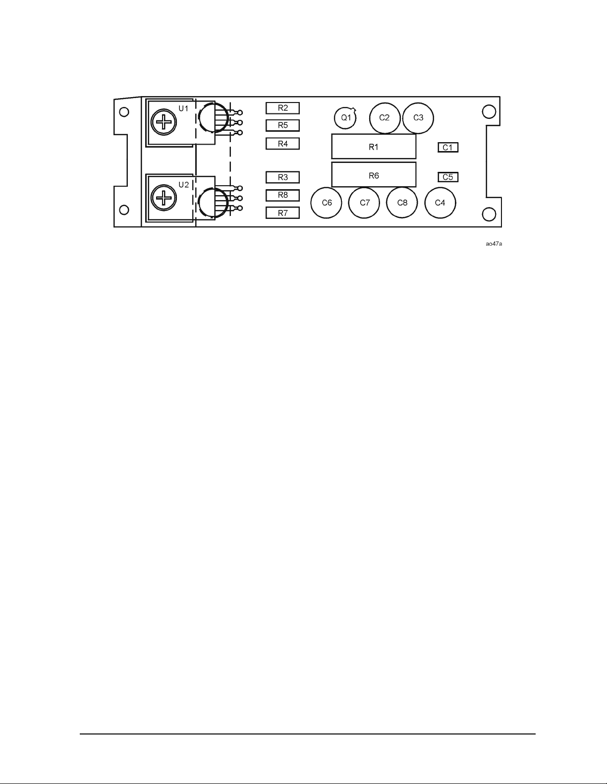
bad, troubleshoot the A1 regulator board. Refer to Figure 7-5 and Figure 7-2 for a
component location diagram and schematic diagram, respectively.
Figure 7-4 Power Supply Check Points
7-6 Chapter7
Page 49
Troubleshooting Procedures
Figure 7-5 A1 Regulator Assembly Component Locations Diagram
Service
Chapter 7 7-7
Page 50

Service
Replacement Procedure
Replacement Procedure
Replacing the Probe Tip
Tools Required:
3/32 inch probe-tip nut driver (supplied with the probe)
10 mm open-end wrench
CAUTION Use static precautions when performing the following procedures. The
amplifier microcircuit is very static sensitive and exposed during this
procedure.
Refer to Figure 7-6.
1. Remove the nut with a 10 mm open-end wrench.
2. Remove the nose assembly, leaving the microcircuit attached to the body of the probe.
CAUTION Failure to remove the nose assembly prior to replacing the tip will result in
damage to the conductive elastometer on the tip assembly.
3. Unscrew the damaged tip with the nut driver and discard the tip.
4. Screw in the new tip and lightly tighten it with a 3/32 inch nut driver.
(Overtightening the tip can damage the nose assembly.)
5. Install the nose assembly and nut. Tighten the nut with a 10 mm open-end wrench.
NOTE The tip on the 10:1 divider can be replaced without disassembling the divider.
Use the 3/32 inch probe tip driver.
Figure 7-6 Probe End Disassembly
7-8 Chapter7
Page 51
Service
Replacement Procedure
Replacing the Amplifier Microcircuit
Tools Required:
10 mm open-end wrench
Small flatblade screwdriver
Refer to Figure 7-6.
1. Remove the nose assembly.
2. Remove the amplifier microcircuit.
Refer to Figure 7-7.
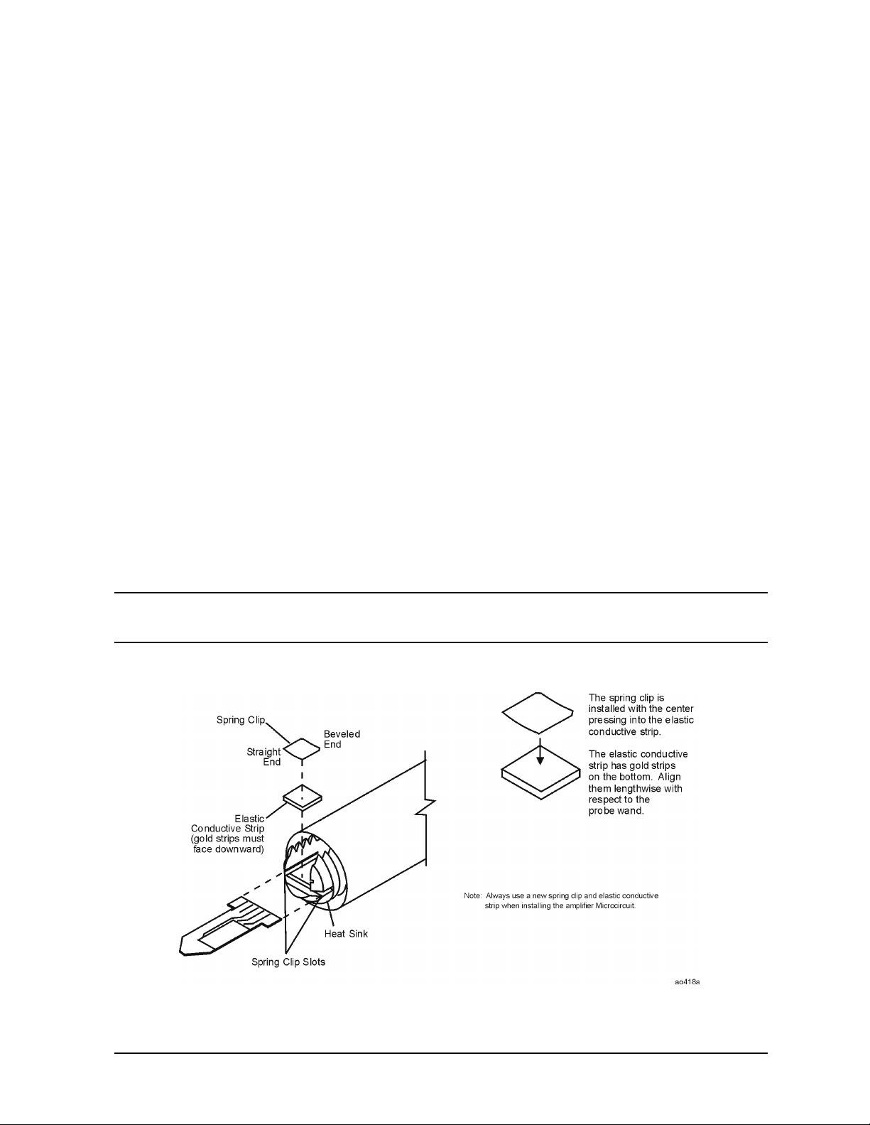
3. Remove and discard the spring clip and elastic conductive strip.
4. Place the new amplifier microcircuit into the probe heatsink. Place the new elastic
conductive strip in place, making sure the gold traces are facing down and are aligned
lengthwise with respect to the probe. Make sure the elastic strip is flush with the front
end of the heatsink. The screwdriver may be used to move the strip.
5. Place the new spring clip over the elastic strip, flush with the front of the heatsink. The
beveled end of the clip should face away from the amplifier microcircuit. The center of
this U-shaped clip must press into the elastic conductor. Insert one side of the clip into
the small slot in the probe heatsink. Press the other side of the clip down with the small
screwdriver until it snaps into the slot on the other side of the heatsink.
6. Replace the nose assembly and nut.
CAUTION Failure to remove the nose assembly prior to replacing the tip will result in
damage to the conductive elastomer on the tip assembly.
Figure 7-7 Probe Wand Components
Chapter 7 7-9
Page 52

Service
Replacement Procedure
Removing the Plastic Regulator Housing Covers
Tools Required:
1/8 inch-wide flatblade screwdriver
WARNING In the steps below, hold the regulator housing and screwdriver so
that you won’t injure yourself if the screwdriver slips.
Refer to Figure 7-8.
1. Hold the regulator assembly by one end and insert the head of a 1/8 inch-wide flatblade
screwdriver into the seam at the other end. The seam separates the two halves of the
housing cover. Twist the screwdriver 90˚.
2. Perform step 1 in several places along the four pry points shown in Figure 7-8.
Reassembling the Covers
3. Replace the metal housing reinforcement and plastic covers as show in Figure 6-1 on
page 6-5. The reinforcement is very important; it ensures that the covers will not pop off
if the unit is dropped.
Figure 7-8 Cover Removal
7-10 Chapter7
Page 53
Service
Replacement Procedure
Replacing the Type-N Output Connector
Tools Required:
9/16 inch open-end wrench
Refer to Figure 7-9.
1. Remove the connector body with the open-end wrench.
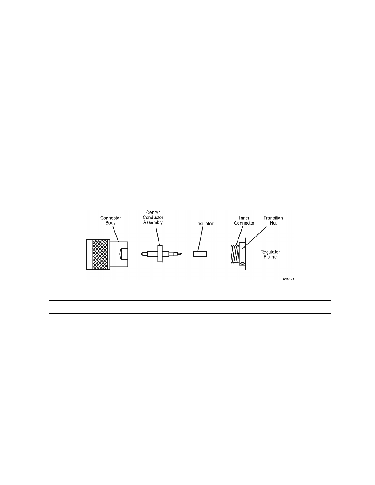
2. Remove the male center conductor assembly from the gold plated inner connector. Use
your fingers to pull out the assembly. The small insulator may or may not come out
attached to the center conductor assembly. If it does, remove it from the old center
conductor assembly and place it on the new one. If it is not attached to the center
conductor assembly (it remained inside the inner connector), proceed to step 3.
3. Hold the new center conductor assembly by the large round insulator, not by the gold
plated center conductor. Carefully align the new center conductor and insert it into the
inner connector. Press gently until you feel it click into place.
4. Place the new connector body and tighten with the open-end wrench.
Figure 7-9 Output Connector Parts
NOTE Refer to “Replaceable Parts” on page 6-4 for part numbers.
Chapter 7 7-11
Page 54

Service
Replacement Procedure
Cable/Probe Wand Replacement
Tools Required:
10 mm open-end wrench
9/16 inch open-end wrench
1/8 inch-wide flatblade screwdriver
Phillips No. 0 or posidrive screwdriver
Long-nose pliers
Special Tool:
Spanner/wrench (part number 85024-20041)
This special tool is pictured in Figure 7-10 on page 7-13.
Refer to Figure 7-6.
1. Remove the nut with a 10 mm open-end wrench.
2. Remove the nose assembly and set aside.
CAUTION The amplifier microcircuit is very sensitive to static electricity. Exercise full
anti-static precautions and use great care when performing the procedure.
Refer to Figure 7-7.
3. Remove the amplifier microcircuit. Remove the spring clip and elastic conductive strip.
Place the microcircuit in a static-safe place. It will be needed later in this procedure.
4. Remove the regulator housing covers by performing the procedure in “Removing the
Plastic Regulator Housing Covers” on page 7-10
Refer to Figure 7-9.
5. Remove the connector body with the 9/16 inch wrench.
Refer to Figure 7-11.
6. Remove the four screws which hold in the regulator assembly. Desolder the colored
wires attached to the regulator assembly and remove the regulator assembly.
7. Remove the transition nut with the transition nut spanner (shown in Figure 7-10) and
pull the inner connector out of its keyed hole.
8. Unscrew the inner connector from the RF cable. Hold the nut with long nose pliers
while turning the connector.
9. Remove the hex nut with the special cable nut wrench (shown in Figure 7-10). The cable
will now come loose.
10.Insert the new cable into the regulator frame and attach the hex nut.
11.Make sure the insulator (shown in Figure 7-9) is inside the connector.
7-12 Chapter7
Page 55

Service
Replacement Procedure
12.Screw the inner connector onto the new RF cable and insert the inner conductor into
the keyed hole.
13.Attach the transition nut with the spanner wrench.
14.Screw on the connector body and tighten with the 9/16 inch wrench.
15.Solder the seven power supply wires onto the regulator assembly as shown in
Figure 7-11.
16.Attach the A1 regulator assembly to the metal frame with the four screws removed
earlier. The long screws go into the heatsink end.
17.Replace the metal housing reinforcement and plastic covers. The covers and housing
reinforcement are illustrated in the replaceable part chapter, in Figure 6-1 on page 6-5.
Refer to Figure 7-7.
18.On the new probe wand, place the amplifier microcircuit into the heatsink assembly.
Place the elastic conductive strip in place, making sure the gold traces are facing down
and are aligned lengthwise with respect to the probe. Make sure the elastic conductor is
flush with the front of the heatsink. The screwdriver may be used to align the strip.
19.Place the spring clip over the conductive strip, flush with the front of the heatsink. The
beveled end of the clip should face away from the front of the wand. The center of this
U-shaped clip must press into the elastic conductor. Insert one side of the clip into the
small slot in the probe heatsink. Press the other side of the clip down with the small
screwdriver until it snaps into the other slot.
Refer to Figure 7-6.
20.Replace the nose assembly and nut.
Figure 7-10 Special Spanner/Wrench Tool and Area of Use
Chapter 7 7-13
Page 56

Service
Replacement Procedure
Figure 7-11 Regulator Parts and Wiring
7-14 Chapter7
Page 57

Connector Inspection and Cleaning
Connector Inspection and Cleaning
The following is a brief introduction to the fundamentals of proper connector care.
Proper connector care is essential to making accurate valid measurements.
Inspecting the Connectors
Visual and mechanical inspection of the output connector and adapter should be done
periodically.
CAUTION If a bad connector is accidentally attached to a good connector, the good
connector can be damaged.
A connector is bad if one of the following conditions exist:
• It fails the visual examination.
Service
• Connectors do not mate smoothly.
Visual Examination
A careful visual inspection should be done often on all device connectors. Vigilance can
save money and ensure the best measurements with your equipment.
Examine the connectors for such obvious problems as deformed threads, contamination, or
corrosion, concentrating especially on the contacting surfaces. Look for burrs, scratches,
rounded shoulders and similar signs of wear and damage. Any problem you can see is
sufficient to cause degraded performance.
Cleaning Connectors
CAUTION Always wear an anti-static wrist strap and work on an anti-static bench mat
when cleaning the probe’s outer connectors. Cleaning a connector requires
you to touch the center conductor of the connector with a swab. The danger of
introducing static electricity into the output connector center conductor must
be completely eliminated. Do not clean the adapter when it is connected to
the probe.
Clean connectors are essential for ensuring the integrity of RF and microwave coaxial
connections. Use the following procedure to clean the connectors in this kit:
1. Use Compressed Air or Nitrogen
Use compressed air (or nitrogen) to loosen particles on the connector mating plane
surfaces. Clean air cannot damage a connector, or leave particles or residues behind.
Chapter 7 7-15
Page 58

Service
Connector Inspection and Cleaning
WARNING Always use protective eyewear when using compressed air or
nitrogen.
You can use any source of clean, dry, low-pressure compressed air or nitrogen that has
an effective oil-vapor filter and liquid condensation trap placed just before the outlet
hose. Ground the hose nozzle to prevent electrostatic discharge, and set the air pressure
to less than 414 kPa (60 psi) to control the velocity of the air stream. High-velocity
streams of compressed air can cause electrostatic effects when directed into a connector.
2. Clean the Connector Threads
Use a lint-free swab or cleaning cloth moistened with isopropyl alcohol to remove any
dirt or stubborn contaminants on a connector that cannot be removed with compressed
air or nitrogen.
a. Apply a small amount of isopropyl alcohol to the lint-free cleaning swab.
b. Clean the connector threads.
c. Let the alcohol evaporate, then blow the threads dry with a gentle stream of clean,
low-pressure compressed air or nitrogen.
WARNING Isopropyl alcohol is extremely flammable, causes irritation, may
cause eye damage, and is harmful if swallowed or inhaled. It may be
harmful if absorbed through the skin. Keep away from heat, sparks,
and flame. Avoid contact with eyes, skin, clothing. Avoid breathing
vapor. Keep in tightly closed container. Use with adequate
ventilation. Wash thoroughly after handling. In case of fire, use
alcohol foam, dry chemical, or carbon dioxide: water may be
ineffective. In case of spill, soak up with sand or earth. Flush spill
area with water.
Dispose of isopropyl alcohol in accordance with all applicable
federal, state, and local environmental regulations
3. Clean the Mating Plane Surfaces
Apply a small amount of isopropyl alcohol to a new swab and clean the center and outer
conductor mating plane surfaces. When cleaning a female connector, avoid snagging the
swab on the center conductor contact fingers by using short strokes.
4. Dry the Connector
After cleaning, blow the connector dry with a gentle stream of clean compressed air or
nitrogen. Always completely dry a connector before you reassemble or use it.
5. Reinspect
Inspect the connector again to make sure that no particles or residue are present.
7-16 Chapter7
Page 59

Table 7-1 Agilent Technologies Sales and Service Offices
UNITED STATES
Instrument Support Center
Agilent Technologies
(800) 403-0801
EUROPEAN FIELD OPERATIONS
Service
Connector Inspection and Cleaning
Headquarters
Agilent Technologies S.A.
150, Route du Nant-d’Avril
1217 Meyrin 2/ Geneva
Switzerland
(41 22) 780.8111
Great Britain
Agilent Technologies Ltd.
Eskdale Road, Winnersh
Triangle Wokingham, Berkshire
RG41 5DZ England
(44 118) 9696622
Headquarters
Agilent Technologies
3495 Deer Creek Rd.
Palo Alto, CA 94304-1316
USA
(415) 857-5027
Japan
Agilent Technologies Japan, Ltd.
Measurement Assistance Center
9-1, Takakura-Cho, Hachioji-Shi,
Tokyo 192-8510, Japan
TEL (81) -426-56-7832
FAX (81) -426-56-7840
France
Agilent Technologies France
1 Avenue Du Canada
Zone D’Activite De Courtaboeuf
F-91947 Les Ulis Cedex
France
(33 1) 69 82 60 60
INTERCON FIELD OPERATIONS
Australia
Agilent Technologies Australia Ltd.
31-41 Joseph Street
Blackburn, Victoria 3130
(61 3) 895-2895
Singapore
Agilent Technologies Singapore
(Pte.) Ltd.
150 Beach Road
#29-00 Gateway West
Singapore 0718
(65) 291-9088
Germany
Agilent Technologies GmbH
Agilent Technologies Strasse
61352 Bad Homburg v.d.H
Germany
(49 6172) 16-0
Canada
Agilent Technologies (Canada) Ltd.
17500 South Service Road
Trans-Canada Highway
Kirkland, Quebec H9J 2X8
Canada
(514) 697-4232
Taiwan
Agilent Technologies Taiwan
8th Floor, H-P Building
337 Fu Hsing North Road
Taipei, Taiwan
(886 2) 712-0404
China
China Agilent Technologies
38 Bei San Huan X1 Road
Shuang Yu Shu
Hai Dian District
Beijing, China
(86 1) 256-6888
Chapter 7 7-17
Page 60

Index
Numerics
1 dB compression
10 to 1 divider
A
A1 regulator assembly
replaceable parts
accessories
adapter, probe
anti-static precautions
average noise level
C
cable/probe wand replacement
7-12
calibration, response
characteristics
10 to 1 divider
general
high frequency probe
probe adapter
supplemental
cleaning
10 to 1 divider
connectors
probe adapter
conditions, environmental
connector
cleaning
inspection
mating
pin-outs
type-N replacement
visual examination
D
description
10 to 1 divider
average noise level
gain at 500 MHz/frequency
gain compression
median gain
probe adapter
description, product
devices
grounding
divider, 10 to 1
E
environmental conditions
environmental requirements
equipment
recommended test
, 1-6
, 7-15
, 3-4
, 3-3
response flatness
, 5-6
, 2-5
, 6-6
, 2-1
, 2-4
, 1-3
, 5-8
, 5-4
, 2-5
, 1-5
, 2-4
, 1-5
, 2-5
, 7-15
, 2-4
, 1-6
, 7-15
, 7-11
, 7-15
, 2-5
, 5-8
, 5-5
, 5-6
, 5-5
, 2-4
, 1-4
, 4-3
, 2-5
, 1-6
, 5-3
,
, 1-6
equipment required for
troubleshooting
equivalent power
external power supply
F
failure
electrical
mechanical
protective sleeve
frequencyresponserelative to 500
G
gain at 500 MHz
gain compression
general information
grounding devices
H
high frequency probe
I
initial inspection
input voltage for 1 dB
input voltage tolerances
inspection
10 to 1 divider
initial
probe adapter
installation
M
mating connectors
measurement precautions
measurements
mechanical failure of the
median gain
N
network analyzer
operation
operator’s check
noise level, average
O
operating characteristics
10 to 1 divider
high frequency probe
probe adapter
operating instructions
discharging the probe
, 7-4
MHz
, 5-5
compression
, 3-2
, 3-1
protective sleeve
, 5-5
, 5-4
, 7-2
, 5-7
, 3-3
, 7-4
, 7-4
, 5-5
, 5-6
, 1-1
, 4-3
, 1-5
, 3-2
, 5-6
, 1-2
, 2-5
, 2-4
, 3-4
, 1-2
, 5-4
, 7-4
, 4-4
, 5-8
, 2-5
, 1-5
, 2-4
, 4-3
, 4-3
extending the protective sleeve,
4-3
grounding the probe
retracting the protective sleeve
4-3
operating, precautions
operation, network analyzer
5-4
operator’s check
network analyzer
spectrum analyzer
P
parts
identification
miscellaneous
replaceable
performance tests
average noise level
gain at 500 MHz/frequency
response flatness
input voltage for 1 dB
compression
median gain
pin-outs, power connector
power connectors
power supply
check
external
high frequency probe
requirements
precautions
anti-static
ESD
measurement
operating
preparation for use
probe
adapter
check power supply
discharging between
measurements
electrical failure
grounding
inspection
mechanical failure
sleeve
tip replacement
visually inspect the tip
probepower supplyrequirements
3-3
procedure
average noise level
gain at 500 MHz/frequency
response flatness
gain compression
, 6-1, 6-5
, 5-5
, 7-4
, 3-3
, 1-3
, 1-3
, 4-2
, 2-4
, 4-3
, 2-4
, 4-3
, 4-3
, 3-3
, 4-1,
, 4-4
, 4-4
, 4-5
, 6-5, 6-6
, 6-3
, 5-1
, 5-8
, 5-5
, 5-6
, 3-3
, 3-3
, 3-3
, 3-3
, 1-2
, 3-3
, 7-4
, 4-3
, 7-4
, 7-4
, 2-6, 7-8
, 7-4
, 5-8
, 5-5
, 5-6
,
,
Index 1
Page 61

Index
input voltage for 1 dB
compression
median gain
operator’s check
operator’scheckusinga network
analyzer
operator’s check using a
spectrum analyzer
replacement
troubleshooting
product
10 to 1 divider
probe adapter
product description
average noise level
gain at 500 MHz/frequency
response flatness
gain compression
median gain
probe adapter
product performance
protective sleeve
extension of
retraction of
R
recommended test equipment
repair strategy
main cable and plastic sleeve
guide
probe tip and amplifier
microcircuit
replaceable parts
A1 regulator assembly
adapter
probe
replacement procedure
amplifier microcircuit
cable/probe wand
plastic regulator covers and
probe tip
type-N connector
required equipment for
requirements
environmental
response calibration
returning the product for service
S
S21 measurement
safe DC input voltage
safe RF input voltage
service
settings
, 2-6
, 2-4, 2-6, 6-4
housing
, 2-6, 7-8
troubleshooting
3-5
, 7-1, 7-17
, 5-6
, 5-5
, 4-4
, 4-4
, 4-5
, 7-8
, 7-4
, 2-5
, 2-4
, 1-4
, 5-8
, 5-5
, 5-6
, 5-5
, 2-4
, 1-5
, 4-3
, 4-3
, 5-3
, 7-2
, 7-2
, 7-2
, 6-1, 6-4
, 6-6
, 7-8
, 7-9
, 7-12
, 7-10
, 7-11
, 7-2
, 1-6
, 5-4
, 5-4
, 1-5
, 1-5
frequency range, 5-4
output power
power meter
specifications, product
performance
spectrum analyzers, operator’s
check
supplemental characteristics
T
test equipment
test procedure
average noise level
gain at 500 MHz/frequency
response flatness
input voltage for 1 dB
compression
median gain
operator’scheckusinga network
analyzer
operator’s check using a
spectrum analyzer
test record
tests, performance
theory of operation
tolerances
electrical
input voltage
transmission measurement
troubleshooting
electrical failure
mechanical failure of the
protective sleeve
power supply
visual inspection of the probe
tip
troubleshooting and repair
troubleshooting equipment
troubleshooting procedure
mechanical failure of the
protective sleeve
power supply
visually inspect the probe tip
7-4
type-N output connector
replacement
V
,
visually inspect the probe tip
voltage
input tolerances
max safe DC input
max safe RF input
W
warranty
, 5-4
, 5-4
, 1-5
, 4-5
, 5-3
, 5-5
, 4-4
, 5-9
, 1-5
, 1-2, 1-5
, 7-1, 7-4
, 7-4
, 7-4
, 7-4
, 7-11
, ii
, 1-5
, 5-8
, 5-5
, 5-6
, 4-5
, 5-1
, 7-3
, 5-4
, 7-4
, 7-4
, 7-1
, 7-2
, 7-4
,
, 7-4
, 1-2, 1-5
, 1-2, 1-5
, 1-2, 1-5
2 Index
 Loading...