

Page 1
Regulating Satellite Bus Voltage
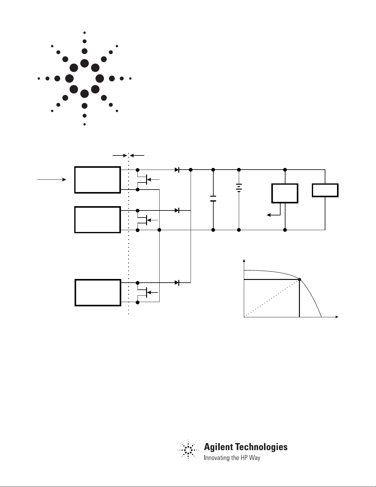
The sequential shunt regulator is
widely used for regulating the satellite
bus voltage. A simplified sequential
shunt concept is shown in Figure 1.
The Agilent Technologies E4350B/
E4351B Solar Array Simulators (SAS)
are ideal for this type of application.
Operating in this mode, the current
either flows into the load or into the
shunt control FETs. The shunt control
FET will be referred to as the shunt
or the switch for the remainder of the
paper. Figure 2 shows a typical solar
array I-V curve. As an example, let’s
assume operation at the maximum
power point. When the shunt is open,
the current to the load will be I
mp
(current at the maximum power
point). When the shunt is closed, the
current in the shunt is I
sc
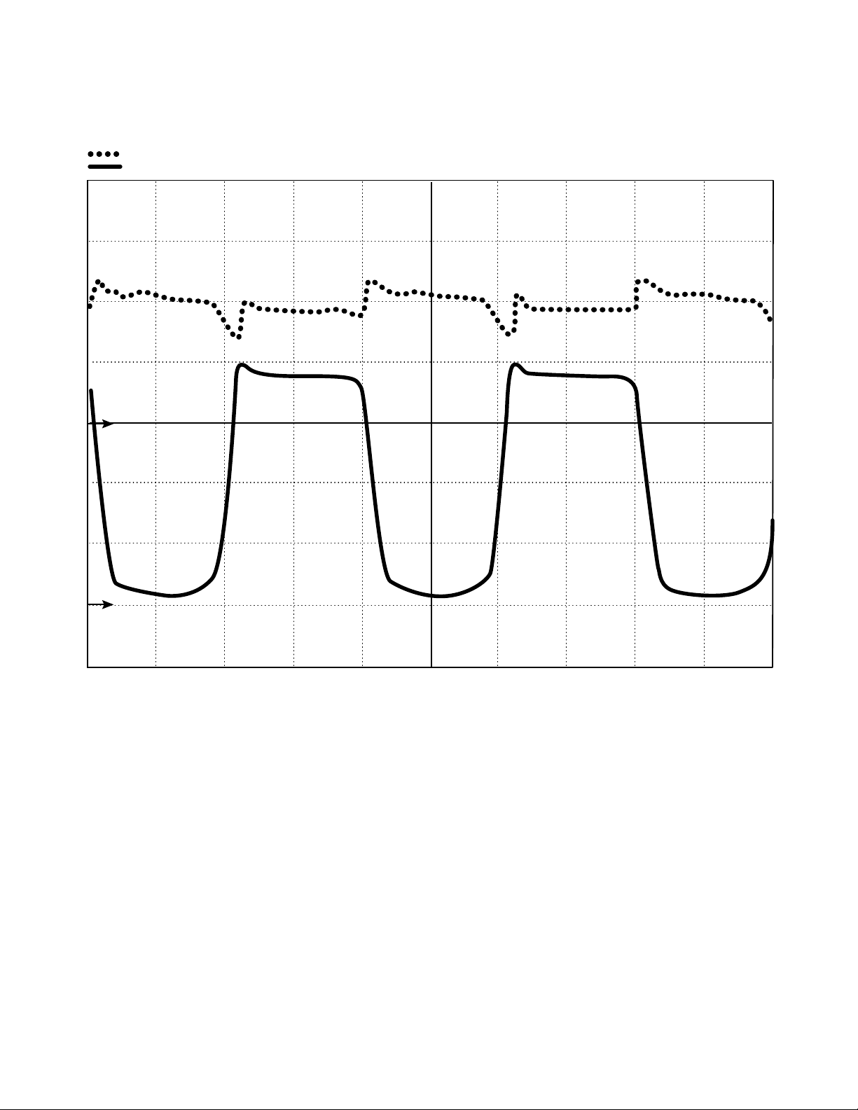
(short circuit current). Figure 3 shows the output waveforms across one SAS. The
output current of the SAS is basically
constant because the difference
between I
mp
and Iscis usually small
but the voltage changes from a short
(switch on) to V
mp
(switch off).
Figure 2
I
sc
= short circuit current
I
mp
= current at the maximum power
V
mp
= voltage at the maximum power
V
oc
= open circuit voltage
P
mp
= maximum power point
R
L
= load line
Agilent AN 1293
Sequential Shunt Regulation
Application Note
SAS #1
GPIB
SAS
Satellite
Control
Control
Control
Bus
Cap
Battery
Control
CKT
Load
Control
Signals
SAS #2
SAS #N
+
-
+
-
+
-
P
mp
R
L
V
mp
VocV
I
sc
I
mp
I
Figure 1
Page 2
2
If bus voltage = V
mp
, then Output
power delivered to the bus = (1-D) (N)
(P
mp
) where: D = On duty cycle of the
shunt FET, N = Number of SAS supplies, P
mp
= Maximum power point.
To satisfy the power demands of the
power system of the satellite, the
output voltage of the SAS has to rise
within 2 to 10 usec when the shunt
is opened and the operating point
changes from the short circuit point
to the operating load point on the
curve. The E4350B/E4351B low
output capacitance (<50 nF) allows
this fast rise time and also limits the
turn on switching losses in the shunt
switch. The E4350B/E4351B can
handle switching frequencies up to
50 KHz. Figure 3 shows the output
voltage and current of the E4351B
when the shunt switches at 50 KHz
with shunt FET rise and fall times of
2 usec. For this test, the E4351B is in
Simulator mode (refer to data sheet)
and the I-V curve defined by these
four parameters: I
sc
= 4.00A, Imp=
3.75A, V
mp
= 120V and Voc=130V.
The wire inductance in the test circuit is very small. As the inductance
increases, the voltage overshoot on
the output voltage will increase, but
will be limited by fast acting internal
clamp circuits. The overshoot and
undershoot in the current (Figure 3)
are due to the internal output snubber, as part of the output capacitance,
charging and discharging. Note that
in Figure 1, the bus capacitor across
the battery is required to smooth the
bus current and lower the ripple.
Figure 3
Channel 1 20.0V/div 60.0000V 10:1 dc 1M ohm
Channel 4 2.00V/div 0.00000V 100:1 dc 50 ohm
0
Sensitivity Position Probe Coupling Impedance
I
OUT 2A/DIV
V
OUT 20/DIV
0
-29.700 US
#AVG
-4.700 US
5.00 US/DIV
20.300 US
Repetitive
Page 3
3
Figure 1 shows diodes in series with
each output of the SAS (after the
shunt). These diodes isolate the supplies so that when one shunt is on,
the output of the other SAS’s is not
pulled low. The diodes should have
very fast recovery time, otherwise the
power dissipation in the diode and
the shunt FET will be high. Higher
levels of noise will also occur if slow
diodes are used, or if the FET rise
and fall times are too fast. The latter
can be controlled by adjusting the
FET gate resistor. Snubber (RC)
across the diodes may help reduce
the switching noise and voltage overshoots. A heatsink may be needed to
keep the diode cool and within the
temperature ratings.
Voltage and current ratings of the
shunt switch are determinedby the
V
oc
and Iscparameters.
The heatsink design for the switch will
depend on the switching frequency
and the duty cycle and the output
current. Higher switching frequency
and higher duty cycle (ON time) will
increase the power dissipation in the
shunt FET.
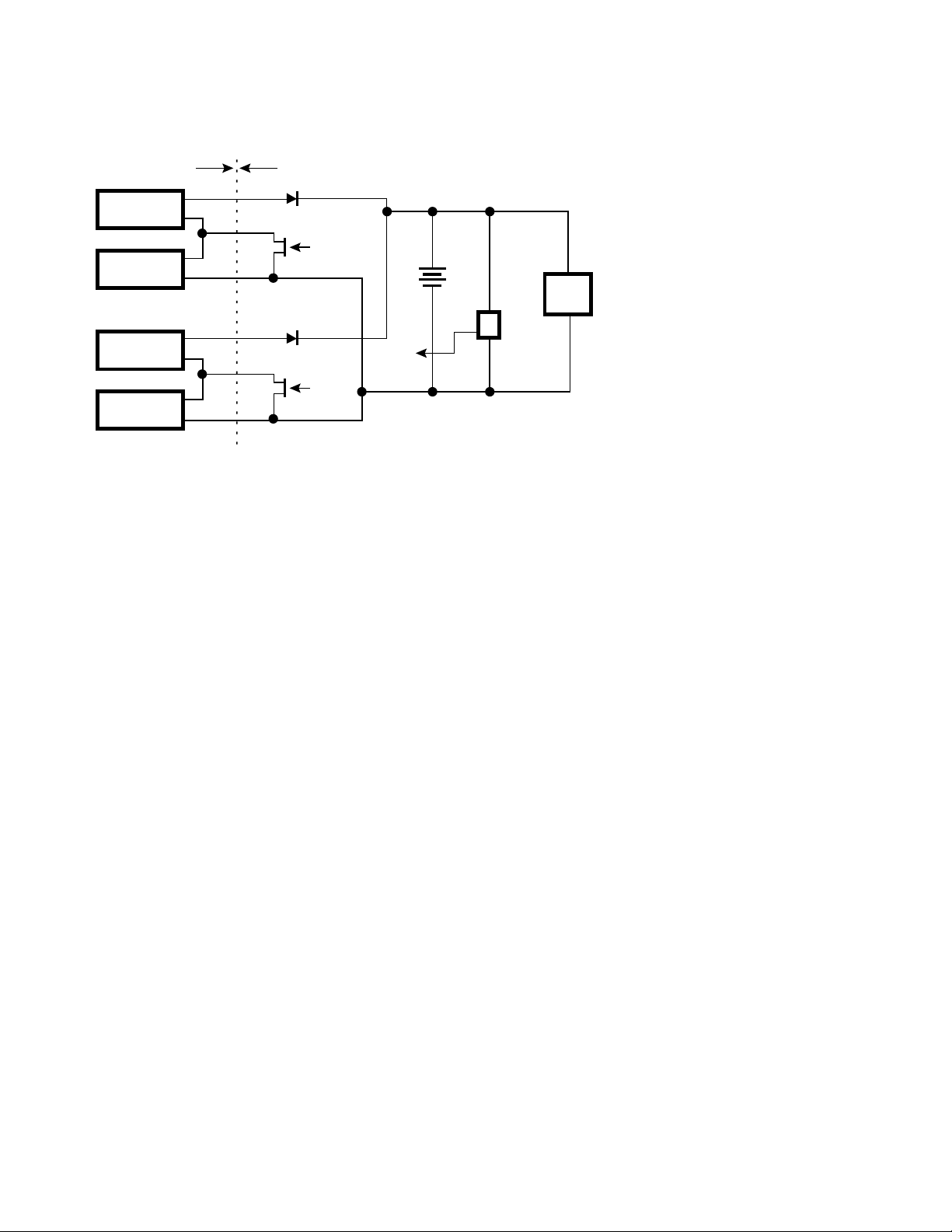
A different sequential shunt that
some customers use is shown in
Figure 4. In this configuration, the
bus voltage cannot be lower than the
output voltage of the upper SAS.
Since only one half of the string is
shunted, the bus voltage will always
have a minimum voltage that is at
least half of the string. The major
advantage of this technique is that it
reduces the power dissipation in the
FET by reducing the switching losses
because the voltage across the FET is
half. It may also make the selection of
the FET easier since a lower voltage
part can be used. Sometimes a linear
device is used instead of a switch in
order to have better control on the
voltage, but this results in higher
power dissipation in the linear
device.
In the sequential shunt configuration,
the number of strings is limited by
the total power required. When using
the E4350B/E4351B, strings may be
added or subtracted as necessary
for the particular application. Each
string is programmable over the
IEEE-488.2 bus using SCPI (standard
commands for programmable instruments) commands.
SAS #1
Figure 4
SAS Satellite
Bus
SAS #2
Control
SAS #n
SAS #n +1
Control
Load
Control
Page 4

By internet, phone, or fax, get assistance
with all your test and measurement needs.
Online Assistance
www.agilent.com/find/assist
Phone or Fax
United States:
(tel) 1 800 452 4844
Canada:
(tel) 1 877 894 4414
(fax) (905) 206 4120
Europe:
(tel) (31 20) 547 2323
(fax) (31 20) 547 2390
Japan:
(tel) (81) 426 56 7832
(fax) (81) 426 56 7840
Latin America:
(tel) (305) 269 7500
(fax) (305) 269 7599
Australia:
(tel) 1 800 629 485
(fax) (61 3) 9272 0749
New Zealand:
(tel) 0 800 738 378
(fax) (64 4) 495 8950
Asia Pacific:
(tel) (852) 3197 7777
(fax) (852) 2506 9284
Product specifications and descriptions in this
document subject to change without notice.
Copyright © 1997, 2000 Agilent Technologies
Printed in U.S.A. 6/00
5965-7329E
 Loading...