

Page 1
Agilent AN 1246
Pulsed Characterization of Power
Semiconductors Using Electronic Loads
Application Note
Electronic Load Improves Power
Semiconductor Measurements
An electronic load eliminates the selfheating problems associated with
measuring the on-state voltage drop
and transconductance (or current
gain) of power semiconductors.
On-state voltage drop and transconductance (or current gain) of power
FETs, BJTs, and IGBTs are temperature dependent, but are typically
specified at 25 °C. However, it is difficult to obtain an accurate measurement of these parameters because the
manufacturer’s test conditions can
cause the device to dissipate significant peak power, which will raise the
device temperature above 25 °C.
Sometimes the amount of peak power
exceeds the device’s static power rating by nearly 6:1! For example, an
IRF540 FET is rated at 150 W continuous, but the transconductance g
specified at a test condition of 17 A
and 50 V, or 850 W. If the device is
subjected to this test condition too
long it will self-heat, and its junction
temperature will no longer be 25 °C,
so measurements will be inaccurate.
is
fs
Electronic Loads
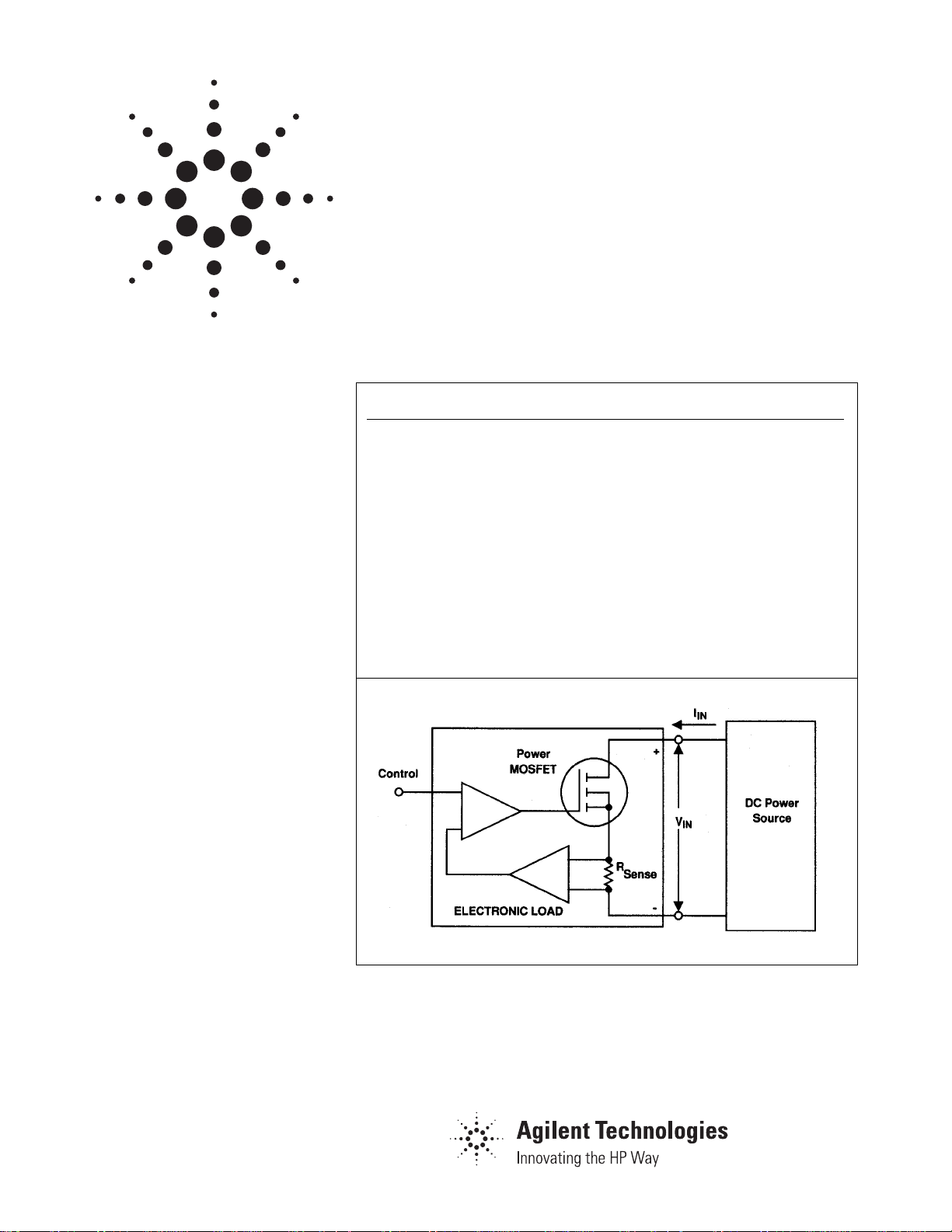
An electronic load (see figure) employs a power MOSFET as an electronically variable load that dissipates power. The electronic load senses MOSFET current (Iin), then amplifies it, compares it with
a reference, and feeds back the output of an error amplifier to the MOSFET gate. This forms a
closed-loop current control system. Therefore, the electronic load’s input current (IIN) is proportional to the control reference input. Input current, IIN, loads the DC power source (battery or power
supply).
Given a fixed control reference, the load acts as a series current regulator. If the control reference
is proportional to the load input voltage (VIN), the load behaves like a high quality power resistor.
Some load manufacturers also offer a constant voltage regulation mode in which the load
behaves like a power zener diode.
Both tests performed in this application use the electronic load’s constant current mode, which is
usually its highest performance mode. Applying the desired pulse waveform to the load’s control
reference input produces the pulsed input (IIN).
Most manufacturers minimize this
problem by characterizing parts with
an 80 µsec (or 300 µsec) current pulse.
If an IRF540 FET is measured at
40 µsec after power is applied, the
Page 2
transient thermal impedance is only
2% of its 1 °C/W DC rating. This
yields a junction-to-case (J-C) temperature rise of only 0.4 °C for measuring R
(on) at 17A (22W peak), but
ds
still yields a J-C rise of 17 °C when
measuring g
(850 W peak). It is not
fs
hard to see why pulsed current measurements are necessary. The narrower
the pulse and faster the measurement, the more accurate the results.
R
(on) is specified at a particular
ds
drain current with a fixed gate voltage. To measure R
(on), bias the gate
ds
with a voltage source, pulse the drain
with rated current, and measure the
drain voltage. R
For the R
ds
(on) is then Vds/Id.
ds
(on) test, a high current
pulse generator with programmable
amplitude, pulse width, repetition
rate, preferably programmable
rise/fall time, with adequate voltage
compliance is needed. A low power
voltage source to set the device under
test (DUT) gate voltage is also needed. Drain voltage is measured at
roughly the mid-point in time of the
drain current pulse, and the ratio of
drain voltage to current is R
ds
(on).
The device transconductance g
is
fs
specified as the incremental drain
current that results from an incremental increase in gate voltage, at a
specified operating drain current.
One method of measuring g
would
fs
be to pulse the gate voltage, apply a
static voltage bias to the drain, and
measure the pulsed drain current. An
alternate method is to apply a static
bias to the gate with the same voltage
source as before, apply a pulsed voltage bias to the drain, and measure
the drain current. For either method
DUT gate voltage is incremented up
from the threshold voltage (V
), and
t
drain current measured at roughly the
mid-point of the pulse until reaching
the specified test current. G
, the
fs
change in drain current for a small
change in gate voltage is then measured
by taking two subsequent measurements, and computing G
= ∆ Id/ ∆ V
fs
.
gs
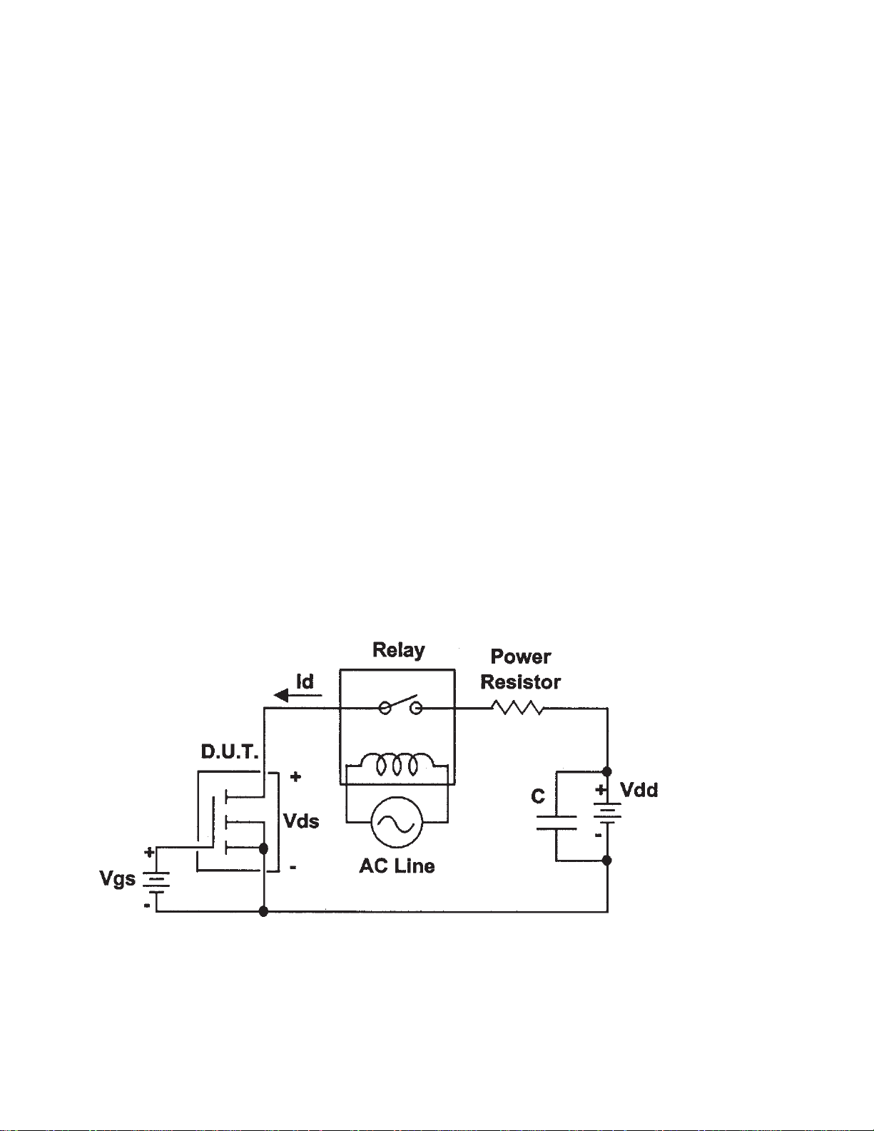
Generating High Current Pulses
At low power levels, self-contained
instruments called SMU’s (stimulusmeasurement units) are readily available for semiconductor device characterization. At high power levels, two
alternate methods to construct SMUequivalent systems can be considered.
An inexpensive, but limited and not
very well-controlled method of generating current pulses is to use a
relay as a switch to connect a voltage
source (V
), current-limiting power
dd
resistor, and the DUT in series as
shown in Figure 1.
An external filter capacitor may be
required across the power supply to
minimize voltage droop during the
high current pulse interval. The relay
is a mercury-wetted type for fast
switching and low contact bounce. It
is alternately closed and opened at a
low repetition rate (typically 60 Hz).
The circuit is designed to produce a
300 µsec test pulse. One disadvantage
of this implementation for the R
ds
(on)
measurement is that the test current
is dependent on power supply voltage
and power resistor value. Therefore,
the resistor and possibly the power
supply voltage need to be reselected
for each test current condition. This
is a laborious approach to obtain a
full set of device characterization data.
In addition, resistance temperature
coefficient and stability can be significant error sources at these power
levels. Also, relay contacts may wear
and fail prematurely when subjected
to repeated high current stresses.
Figure 1. Current pulse generator using a
relay switch for parameter measurement.
2
Page 3
The power supply voltage (V
) allows
dd
enough voltage drop for the DUT onstate voltage of Id*R
ds(on)
, the minimum required load operating voltage.
This is the voltage needed to drive
the wiring inductance and any supply
voltage droop occurring over the
pulse width.
V
= Id* R
dd
ds(on)
+ V
load
+
L•di/dt + droop
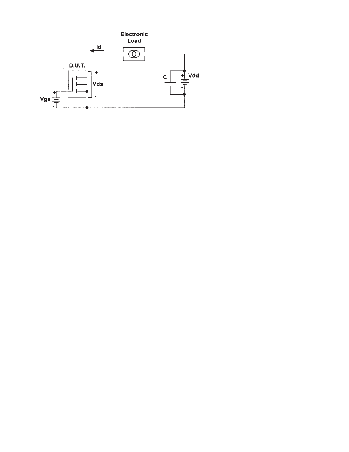
Figure 2. Electronic Load measurement
system.
In Figure 2 the relay and resistor
combinations from Figure 1 are
replaced by an electronic load. The
voltage source, V
is retained to cre-
dd
ate a pulsed constant current source.
An advantage of this approach is
that the electronic load can be reprogrammed for various test currents
without rewiring the circuit. The test
current can be set much more accurately and exhibits little or no temperature dependence or drift, and
there are no mechanical parts to wear
out. In addition, other test current
attributes, such as rise time, can be
programmed to virtually eliminate
the effect of parasitic wiring inductance on test results. Much narrower
pulse widths and variable repetition
rates within the electronic load’s
specifications, can be generated.
Most electronic loads also offer a
"current monitor" signal that produces an analog voltage proportional
to the current drawn. This signal may
be used directly for the current measurement rather than having to add
an accurate, high current shunt or
current probe.
Measuring Rds(on)
Apply the test set-up in Figure 2 to
measure R
MOSFET. The same technique applies
for measuring V
V
ce(sat)
supply replaced by a current source
for the BJT). The gate power supply
is set for the specified 10 V test condition, so the DUT exhibits a low
drain-to-source impedance, and the
electronic load controls the current
drawn from the drain power supply
(V
). Programmed for its constant
dd
current, triggered transient pulse
mode, the electronic load generates a
17 A, 80 µsec pulse with a 2.5 A/µsec
current slew rate. Trigger commands
are sent over GPIB from a BASIC
program at a 5-Hz rep rate to keep
static power dissipation so low (8 mW)
that the test could be run in free air
with no heat sink.
(on) of an IRF540 power
ds
for an IGBT, or
ce(on)
for a BJT (with the Vgspower
The Id*R
(on) term is less than 2 V
ds
at the 17 A test condition. The 6060B
electronic load is specified at 3 V minimum for AC operation. Allowing for
as much as 1 µH wiring inductance
with 2.5 A/µsec slew rate, requires
2.5 V for the L•di/dt term.
Assuming the power supply is too
slow to respond to the instantaneous
high current demand, the required filter capacitor value to limit the supply
voltage droop term to 2 V would be
C = (I
* tw)/∆V = 17 A * 80 µsec/2 V
d
= 680 µF. The 6032B power supply
chosen had adequate internal filter
capacitance, so no external filter
capacitance was required. V
dd
is programmed to 10 V for the test because
the total required minimum power
supply voltage was 9.5 V.
Current was first monitored with a
Textronix AM 503 P6302 current
probe amplifier to verify overall operation. It was not found necessary
for this test because the electronic
load settled within 20 µsec. V
was
ds
monitored at the DUT and fed to an
Agilent 54503A digitizing oscilloscope.
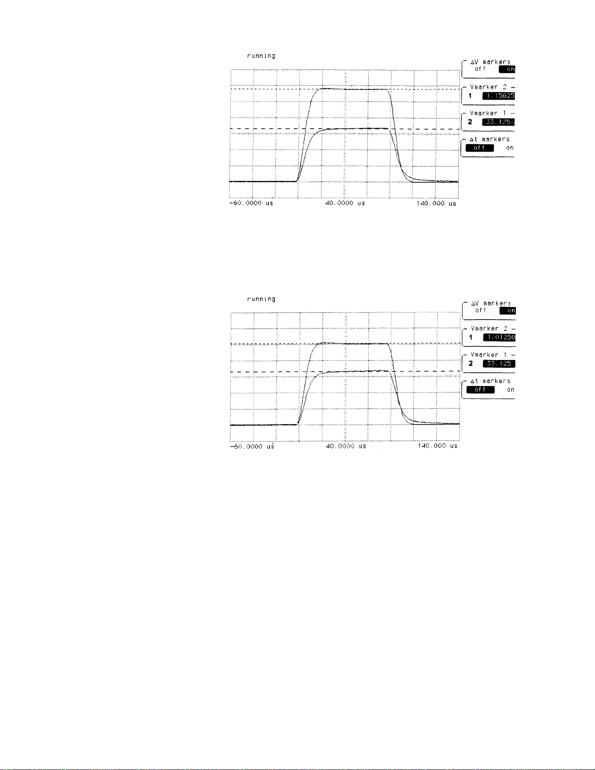
Figure 3 shows the actual waveforms.
R
measured 71 mOhms for this
ds(on)
test sample. The typ/max R
ds(on)
from
the IR data sheet is 60/70 mOhms for
this part, so actual test results fall
within the expected range of values.
3
Page 4
The test was then rerun on the same
test device with the gate voltage raised
from the specified 10 to 15 V, and
R
dropped from 71 to 66 mOhms
ds(on)
(Figure 4). R
vs Idplots for a
ds(on)
fixed gate voltage could also be conveniently acquired with this test
setup. This would allow a power supply designer to understand how much
quantitative thermal benefit has been
gained by driving a MOSFET switch
at a somewhat higher gate voltage. It
would also show what actual losses
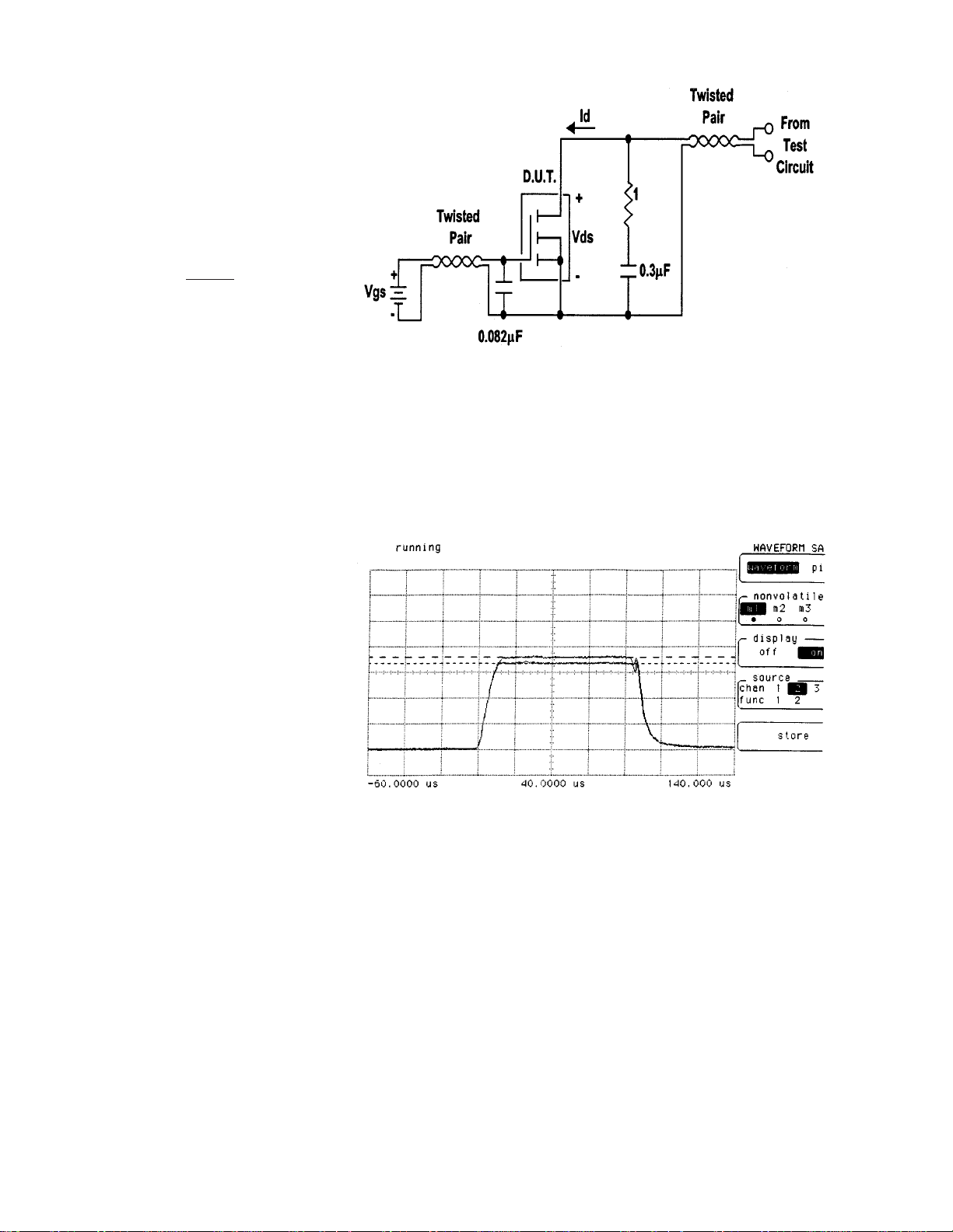
are to be expected at the actual circuit drain current. Even if relatively
short twisted-pair leads are used, bypass capacitors are necessary from
drain-source and gate-source to prevent very high frequency parasitic
oscillations due to test lead length.
Figure 5 shows the actual bypass
scheme used.
Figure 3. Vdsand Idmeasurement waveforms, gate V= 10 V, top trace: V
mV/div, bottom trace: I
at 5A/div, time
d
ds
at 200
base: 20 µsec/div.
MEASURING G
fs
Use the same test set-up given in
Figure 2 to measure gfs for the IRF540
power MOSFET. This technique can be
applied to measuring gfe for an IGBT,
and life for a BJT as well (with the
Vgs power supply replaced by a current source for the BJT). Use the second gfs test method described earlier.
For the gfs test, the electronic load is
essentially used as a switch, to apply
a pulsed drain voltage (V
dd-Vload
). A
gate voltage is established, and the
DUT itself determines the current
that flows based on its threshold voltage and transconductance. To cause
the electronic load to act as a switch,
program its current somewhat above
the test current. For example, 22 A
for a 17 A test current. This forces
the load into an unregulated condition, where it asks to draw more current than the DUT will allow. Slew
rate was set at 5 A/µsec for this test.
Figure 4. Vdsand Idmeasurement waveforms, gate voltage=15 V, top trace: V
ds
at 20 mV/div, bottom trace: Idat 5A/div,
time base: 20 µsec/div.
4
Page 5
To measure gfsat the specified test
current and drain voltage it is necessary to first iterate to find the V
gs
that produces the desired test current
for this particular DUT. V
is incre-
gs
mented up from the threshold voltage
(V
) until the desired test current (Id1)
t
is reached at a given V
V
is incremented again and a higher
gs
I
) results. Computing gfs:
d(Id2
)
(I
d2-Idl
g
= (Vg2-Vgl)
fs
gs(Vgs1
). Then
For the IRF540, V
for the test current of 17.9 A, and V
2 measured 6.0 V
gs
gsl
measured 5.9V, at a drain current of
16.7 A. G
was then computed as
fs
roughly 12, which again agrees quite
well with the min/typ values of 8/13
given in the IRF540 data sheet. Figure
6 shows oscilloscope waveforms for
both drain current conditions.
Practical Considerations
To keep from momentarily exceeding
the maximum power rating of the 300 W
electronic load, set the power supply
voltage (V
for the gfs test. The drain-source bypass capacitance (Figure 5), added to
prevent high-frequency oscillation of
the DUT, limits how fast the drain
voltage can increase. Therefore, it
places the maximum voltage across
the electronic load with full current
for the first part of each test pulse
(approximately 20 µsec for test condi-
tions listed). Because g
weak function of V
lower V
the test results. This was confirmed
by observing no change at all in drain
current when varying Vds from 20
to 50 V.
) to 30 V rather than 50 V
dd
is a very
fs
, testing at the
had no significant effect on
ds
ds
Figure 5. Capacitor bypass circuit.
Figure 6. Drain current, top trace: Id2, bottom trace: I
, top/bottom trace: 5A/div,
d1
time base: 20 µsec/div.
5
Page 6
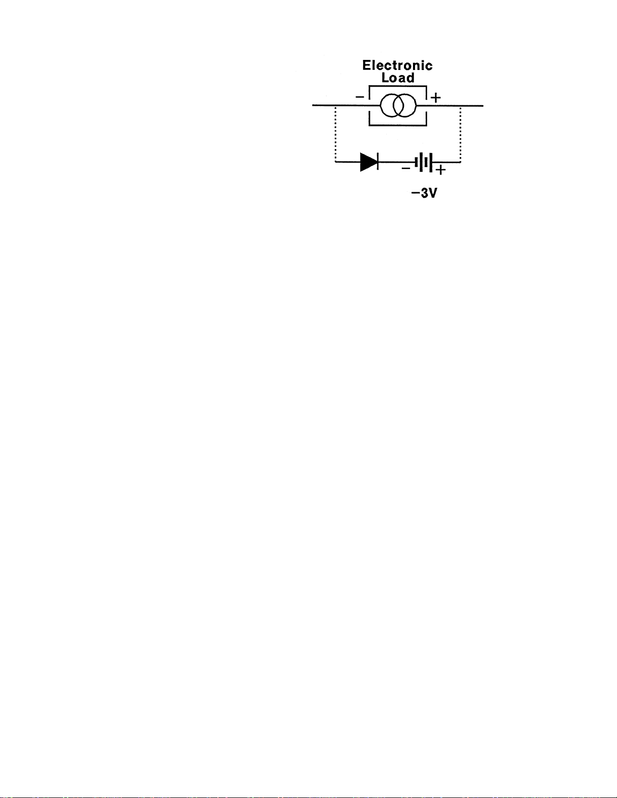
To keep the load voltage above its
minimum specified operating voltage,
connect a power supply and diode
combination (Figure 7) across the
electronic load for the g
test. The
fs
load functions as a switch for this
test, unlike the R
(on) test where the
ds
load itself regulates the DUT current.
Actual pulse-width will exceed programmed pulse-width by approxi-
mately 15 µsec if the 6060B load volt-
age falls below its minimum voltage
specification. This occurs because the
load becomes unregulated, and takes
some additional time to recover from
this condition. Depending on how
accurate pulsewidth control needs to
be, the additional power supply and
diode combination may be eliminated
with no other observed side effects.
Some necessary attributes of the
electronic load are:
• Minimal overshoots and under-
shoots
• Triggered or continuous program-
mable pulse generation
• Graceful recovery from being driv-
en unregulated during the gfs test
(if the additional power supply
and diode combination shown in
Figure 7 are not used).
• Programmable current slew rate,
which allows control over L di/dt
voltage spikes and minimizes
ringing
• Rated for the peak power it sees
during the test
Figure 7. Power supply and diode combination.
For the R
(on) test, peak power can
ds
be minimized by setting the drain
voltage supply (V
the g
test, the load only sees peak
fs
) fairly low. For
dd
power during the transitions, because
the DUT itself sees full power during
measurement. Peak load power can
be minimized by minimizing test lead
lengths and inductance, so a small
drain bypass capacitor can be used
(Figure 5).
Other useful Load features are an
"Imon" analog current port so that a
separate current shunt or current
probe is not required. However, some
flexibility is lost when using the
internal load shunt, because measurement common constraints and fixture
bypass capacitor currents (Figure 5)
needs to be considered. A trigger-out
feature for test stimulus and measurement synchronization is useful,
though the trigger features on the
oscilloscope used were adequate. A
load trigger-in feature allows another
load to be used to create pulsed
rather than static base current for
testing BJTs. This is synchronized
with the collector test current, thereby minimizing heating in both the
base and collector regions of the DUT.
The 6060B load used for these tests
had both the necessary and useful
features, and all required performance
attributes. As seen in Figures 3, 4,
and 6, current and voltage waveforms
are particularly clean and well-controlled, making it possible to perform
the desired pulsed measurements.
6
Page 7

By internet, phone, or fax, get assistance
with all your test and measurement needs.
Online Assistance
www.agilent.com/find/assist
Phone or Fax
United States:
(tel) 1 800 452 4844
Canada:
(tel) 1 877 894 4414
(fax) (905) 206 4120
Europe:
(tel) (31 20) 547 2323
(fax) (31 20) 547 2390
Japan:
(tel) (81) 426 56 7832
(fax) (81) 426 56 7840
Latin America:
(tel) (305) 269 7500
(fax) (305) 269 7599
Australia:
(tel) 1 800 629 485
(fax) (61 3) 9210 5947
New Zealand:
(tel) 0 800 738 378
(fax) (64 4) 495 8950
Asia Pacific:
(tel) (852) 3197 7777
(fax) (852) 2506 9284
Product specifications and descriptions in this
document subject to change without notice.
Copyright © 1993, 2000 Agilent Technologies
Printed in U.S.A. 9/00
5091-7636E
 Loading...