

Page 1

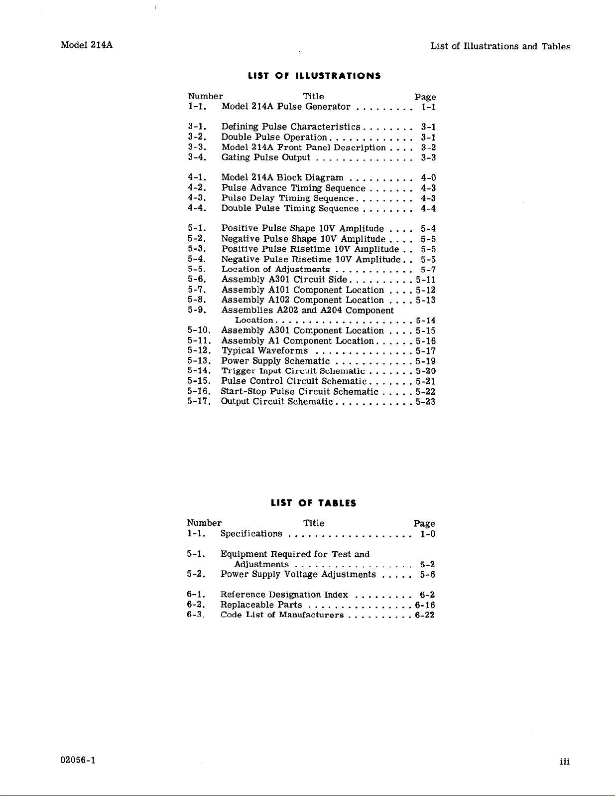
5 OPERATING
f
‘\
AND SERVICE
GENERATOR
MANUAL
214A
HEWLETT
m
-meT&~c~~R~
Y
Page 2

COPYRIGHT AND DISCLAIMER NOTICE
Copyright - Agilent Technologies, Inc. Reproduced with the permission of Agilent
Technologies Inc. Agilent Technologies, Inc. makes no warranty of any kind with regard
to this material including, but not limited to, the implied warranties of merchantability
and fitness for a particular purpose. Agilent Technologies, Inc. is not liable for errors
contained herein or for incidental or consequential damages in connection with the
furnishing, performance, or use of this material or data.
Page 3

CERTIFICATION
The Hewlett-Packard Company certifies that this instrument was
thoroughly tested and inspected and found to meet its published
specifications when it was shipped from the factory. The Hewlett-
Packard Company further certifies that its calibration measurements
are traceable to the U. S. National Bureau
allowed by the Bureau’s calibration facility.
of
Standards to the extent
WARRANTY AND ASSISTANCE
All Hewlett-Packard products are warranted against defects in
materials and workmanship. This warranty applies for one year from
the date of delivery, or, in the case of certain major components listed
in the operating manual, for the specified period. We will repair or
replace products which prove to be defective during the warranty
period. No other warranty is expressed or implied. We are not liable
for consequential damages.
For any assistance contact your nearest Hewlett-Packard Sales and
Service Office. Addresses are provided at the back of this manual.
Page 4

OPERATING AND SERVICE MANUAL
MODEL 214A
PULSEGENERATOR
SERIALS PREFIXED: 812.
02056-7 PRINTED: APR 1968
Page 5

Table of Contents Model 214A
TABLE OF CONTENTS
Section Page
I GENERAL INFORMATION. ........... l-l
l-l. Instrument Description ......... l-l
l-5. Instrument Applications ........ 1-2
1-7.
Equipment and Accessories
Available ................ l-2
l-9. Differences Between Instruments . . l-2
II PREPARATION FOR USE
2-l. Initial Inspection .............
2-3. AC Power Considerations
............
.......
2 - 1
2 - 1
2-l
2-4. Power Source Requirements ... 2-l
2-6.
Three-Conductor Power Cable . . 2-l
2-8. Ventilation Requirements ....... 2 -1
2-11. Rack/Bench Conversion ........
2-l
2-15. Repackaging for Shipment ....... 2 -1
2-16. Packaging Suggestions ....... 2 -1
2-18.
Returning for Service or Repair . 2-2
III OPERATING INSTRUCTIONS .......... 3-l
3-l. General ................... 3-l
3-3. Operating Considerations ....... 3 - 1
3-4. Duty Cycle Limitation. .......
3-l
3-7. Pulse Position vs. Rate ...... 3-l
3-9. Minimum Spacing with Double
Pulses ................
3-3
3-11. Gating of Pulses ........... 3-3
3-13. Operating Procedures. .........
3-3
3-14. Manual Trigger Mode ........ 3-3
3-16. External Trigger Mode ....... 3-3
3-18. Internal Trigger Mode ....... 3-3
IV PRINCIPLES OF OPERATION
.........
4-1
4-l. General ................... 4-1
4-3. Input and Rate Generator. ....... 4-l
4-4. External Trigger Operation .... 4-1
4-7. Manual Trigger Operation ..... 4-l
4-9. Internal Trigger Operation
.... 4-1
4-11. Trigger Blocking Oscillator. ... 4-l
4-13.
Gate Input Circuit ............
4-2
4-15. Advance, Delay, Double Pulse
4-17.
Modes ..................
Pulse Position Circuit .......
4-2
4-2
4-20. Pulse Width Multivibrator ..... 4-2
4-22.
Trigger Output Blocking
Oscillator. ............. 4-2
4-24. Start-Stop Pulse Blocking
Oscillators ............. 4-2
4-27. Pulse Advance Timing Logic ...
4-2
APPENDIX I MANUAL CHANGES. * . * . * * . * . * . I-l
Section
Page
4-29. Pulse Delay Timing Logic ..... 4-2
4-31. Double Pulse Timing Logic
.... 4-3
4-33. Forming and Controlling Output
Pulse. .................. 4-3
4-35. Start Pulse Spiker .......... 4-3
4-37. Stop Pulse Spiker. .......... 4-4
4-39. Pulse Output Circuit. ........ 4-4
4-41.
Pulse Output Amplitude Controls. 4-4
4-43. Reversing Pulse Polarity. ..... 4-4
V MAINTENANCE .................. 5-l
5-l. Introduction ................ 5-l
5-3. Performance Check ........... 5-l
5-5.
External Gating ............
5-l
5-6. External Triggering ......... 5-l
5-7. Pulse Amplitude and Width
.... 5-l
5-8. Pulse Position. ............ 5-2
5-9.
Double Pulse and Manual
Triggering ............. 5-3
5-10. Internal Rep Rate. ..........
5-3
5-11. Duty Cycle ............... 5-3
5-12. Pulse Droop .............. 5-4
5-13.
Overshoot, Preshoot, and Pulse
Top Variation ........... 5-4
5-14.
Rise Time and Fall Time
..... 5-4
5-15. Rate and Width Jitter ........ 5-5
5-16. Output Pulse to Trigger Output
Jitter ................ 5-6
5-17. Adjustments ................ 5-6
5-21. Power Supply Adjustment ..... 5-6
5-23. Rate Multivibrator .......... 5 -6
5-24.
Pulse Position Multivibrator
... 5-7
5-25. Output Bias Current ......... 5-8
5-26.
Pulse Width and Amplitude
.... 5-8
5-27. Overload Relay Adjust ....... 5-10
5-28. Troubleshooting. .............
5-10
5-30. Trigger Mode Checks ........ 5-10
5-31. Pulse Control Checks
5-32.
Output Circuit Checks.
........ 5-10
....... 5-10
5-33. Power Supply Checks ........ 5-11
5-35. Repair and Replacement
....... .5- 11
5-36. General ................. 5-11
5-38. Servicing Etched Circuit Boards. . 5- 11
5-40. Periodic Maintenance .......... 5-11
5-41. General ................. 5-11
5-43. Cleaning Air Filter ......... 5-11
VI REPLACEABLE PARTS .............
6-l
6-l. Introduction ................ 6-l
6-4. Ordering Information .......... 6-l
ii
02056-3
Page 6
Model 214A List of Illustrations and Tables
LIST OF ILLUSTRATIONS
Number Title
Page
l-l. Model 214A Pulse Generator ......... l-1
3-1.
Defining Pulse Characteristics. ....... 3-l
3-2, Double Pulse Operation ............. 3 - 1
3-3. Model 214A Front Panel Description .... 3-2
3-4. Gating Pulse Output ............... 3-3
4-l. Model 214A Block Diagram ..........
4-O
4-2. Pulse Advance Timing Sequence ....... 4-3
4-3. Pulse Delay Timing Sequence. ........ 4-3
4-4. Double Pulse Timing Sequence ........ 4-4
5-l.
5-2.
5-3.
5-4.
5-5.
5-6.
5-7.
5-8.
5-9.
5-10.
5-11.
5-12.
5-13.
5-14.
5-15.
5-16.
5-17.
Positive Pulse Shape 1OV Amplitude
Negative Pulse Shape 1OV Amplitude .... 5-5
Positive Pulse Risetime 1OV Amplitude . . 5-5
Negative Pulse Risetime 1OV Amplitude. . 5-5
Location of Adjustments ............
Assembly A301 Circuit Side. ......... 5-11
Assembly Al01 Component Location
Assembly Al02 Component Location .... 5-13
Assemblies A202 and A204 Component
Location.
....................
Assembly A301 Component Location
Assembly Al Component Location. ..... 5-16
Typical Waveforms ............... 5-17
Power Supply Schematic ............
Trigger Input Circuit Schematic ....... 5-20
Pulse Control Circuit Schematic.
Start-Stop Pulse Circuit Schematic ..... 5-22
Output Circuit Schematic. ...........
.... 5-4
5-7
.... 5-12
5-14
.... 5-15
5-19
...... 5-21
5-23
02056-l
LIST OF TABLES
Number Title Page
l-l. Specifications . . . . . . . . . . . . . . . . . . . 1-O
5-l. Equipment Required for Test and
Adjustments . . . . . . . . . . . . . . . . . . 5-2
5-2. Power Supply Voltage Adjustments . . , . . 5-6
6-l. Reference Designation Index . . . . . . . . . 6-2
6-2. Replaceable Parts . . . . . . . . . . . . . . . . 6-16
6-3. Code List of Manufacturers . . . . . . . . . . 6-22
. . .
111
Page 7

Section I
Table l-l
Model 214A
Table l- 1. Specifications
1
OUTPUT PULSE
Source Impedance:
lower ranges: approximately 1500 ohms on the
lOO-volt range.
Pulse Shape
Rise and Fall Time: <13 nsec on 20-volt and
lower ranges and the -50 volt range, < 15 nsec
on the +50 volt range.
with vernier set for maximum attenuation.
1OOV range typically 15 nsec.
Pulse Amplitude:
attenuator provides 0.2 to 100 volts in a 1,2,
5, 10 sequence (9 ranges). Vernier reduces
output of 0.2~ setting to 80 mv and provides
continuous adjustment between ranges.
Polarity: Positive or negative.
Overshoot: < 50/o, both leading and trailing edges.
Pulse Top Variations: < 4%.
Droop: < 6%.
Preshoot: < 2%.
Pulse Width: 50 nsec to 10 ms in 5 decade
ranges. Continuously adjustable vernier.
Width Jitter: < .05% of pulse width + 1 nsec.
50 ohms on the 50-volt and
Typically < 10 nsec
100 volts into 50 ohms. An
External
Repetition Rate: DC to 1 MC
Sensitivity: < 0.5~ pk
Slope: Positive or negative
Level: Adjustable from -40~ to +4Ov.
Delay: Delay between input trigger and leading
edge of pulse out is approximately 250 nsec in
Pulse Advance mode (approx. 420 nsec minimum in Pulse Delay mode).
External Gating: +8 volt signal gates pulse gen-
erator on. Maximum signal, +4Ov peak.
Double Pulse
Minimum Spacing: 1 usec on the .05 to lksec
pulse width range.
upper limit of Width range.
Trigger Output
Amplitude: > 1Ov open circuit.
Width: 0.05 psec, nominal.
Polarity: Positive or negative.
GENERAL
Maximum Duty Cycle: 10% on 100 and 50 volt
ranges; 25% on 20 volt range; 50% on 10 volt
and lower ranges.
Power: 115 or 23OvilO%, 50 to 60 cps,
Dimensions:
On all other ranges 25% of
325
watts.
Pulse Position: 0 to 10 ms advance or delay,
with respect to trigger output (5 decade ranges).
Continuously adjustable vernier.
Position Jitter: < 0.05% of advance or delay
setting +l ns (between trigger pulse and output
pulse).
REPETITION RATE AND TRIGGER
Internal
Repetition Rate:
continuously adjustable vernier.
Rate Jitter: < 0.5% of the period.
Manual: Push button single pulse, 2 cps maxi-
mum rate.
10 cps to 1 MC (5 ranges),
Weight:
(19,6 kg).
Net 35 lbs. (15,8 kg). Shipping 48 lbs.
J
1-o
02056-3
Page 8

Model 214A
Paragraphs l-l to l-4
Section I
SECTION I
GENERAL INFORMATION
l-l. INSTRUMENT DESCRIPTION.
1-2. The m@$ Model 214APulseGenerator (Figure l-l)
is a versatile instrument providing variable repetition rate, variable width, variable amplitude, positive or negative, pulses with a rise and fall time of
less than 15 nanoseconds. The complete specifications are given in Table l-l. Pulse power of up to
200 watts is available when using a 50-ohmload. The
Model 214A output impedance matches an external
system of 50 ohms on all ranges of 50 volts amplitude
and below, thus minimizing reflections. The maxi-
mum pulse amplitude is 100 volts (with a source
impedance of 1500 ohms) and the amplitude may be
set as low as 80 millivolts using the vernier and the
lowest range. For pulse amplitudes of 10 volts and
less, the duty cycle may be set as high as 50% (see
Table l-l for duty cycle limits at other amplitudes),
providing a square wave output.
l-3. Pulses may be obtained from the Model 214A
at a rate of dc to 1 MC using an external trigger source
or from 10 cps to 1 MC with an internal generator.
For external triggers, positive or negative signals
of 0.5 volt peak may be used and trigger slope and
level may be selected to determine the triggering
point on the waveform. A single pulse may be obtained
from an internal circuit each time a manual button
is pushed. Gating of pulses is done easily by applying
an external signal and an output occurs only when the
gating signal reaches a positive 8 volt level. Three
modes of pulse operation allow: (1) setting of the
output pulse to occur from 0 to 10 ms before (advance)
the trigger output, (2) setting of the output pulse to
occur from 0 to 10 ms after (delay) the trigger output,
or (3) a double pulse output with variable spacing
between the two pulses.
l-4. The Hewlett-Packard modular instrument enclosure system provides advantages in maintenance
and operation. Easy removal of instrument covers
allows access to all chassis and circuit components.
As a bench type instrument the modular design provides mechanical stability even when several instruments are stacked together. The bench type instrument is readily converted for use in standard width
02056-l
Figure l-l. Model 214A Pulse Generator
l-l
Page 9

Section I
Paragraphs l-5 to l-10
Model 214A
rack using hardware shipped with the instrument.
Paragraph 2-11 explains the details of converting to
either the rack or bench version,
l-5. INSTRUMENT APPLICATIONS.
l-6. With its variable pulse characteristics the
Model 214A is useful as a general purpose laboratory
or production line test instrument.
The high peak
current output available, 2 amps, is useful for testing
current driven devices such as magnetic memory
cores, high power modulators, and power amplifiers.
Fast rise and fall time combined with highpower out-
put pulses facilitate checking switching time of high
power semiconductors. The positiveor negative pulse
output, with identical characteristics, provides an
easy technique for checking either npn or pnp type
transistors. By gating the Model 214A output, a
burst of pulses may be obtained for making computer
logic measurements. The double pulse feature may
also be used for pulse resolution tests of amplifiers
and memory cores.
l-7. EQUIPMENT AND ACCESSORIES
AVAILABLE.
l-8. A complete line of electronic test equipment
is available from the Hewlett-Packard Company for
use in making test measurements with, or maintaining, the Model 214A. Also available are cables,
connectors, adapters and other accessory items for
use in various test or measurement applications.
For information on specific items, consult the &?
Catalog or your @ Field Engineer.
1-9. DIFFERENCES BETWEEN INSTRUMENTS.
l-10. The Hewlett-Packard Company uses a two-
section, eight-digit serial number to identify instruments (e.g. ~-00000). The serial number is located
on a plate attached to the instrument rear panel. The
first three digits are a serial prefix number, also
appearing on the first page of this manual, and the
last five digits identify a specific instrument. If the
serial prefix number of the instrument is higher than
that on the first page, change sheets included with the
manual will define differences between other instru-
ments and the Model 214A described herein. If the
change sheets are missing, your @J Field Engineer
can supply the information. Refer to Appendix I at
the back of this manual for changes required to adapt
this manual to an instrument with a lower serial
prefix.
Page 10

Model 2 14A
SECTION II
PREPARATION FOR USE
2-1.
INIT
IAL INSPECTION.
2-2.
Upon receipt of the Model 214A, verify that
the contents are intact and complete as ordered.
Inspect the instrument for any physical damage such
as a scratched panel surface, broken knob or connector,
possible reshipment,
material if reusable (see Paragraph 2-15), until a
satisfactory operational check (Paragraph 5-3) is
completed. If damage is found, file a claim with
the freight carrier and refer to the warranty page in
this manual. Section V outlines the recommended
adjustment and troubleshooting procedures needed
for normal maintenance or recalibration.
2-3. AC POWER CONSIDERATIONS.
2-4. POWER SOURCE REQUIREMENTS.
2-5. The Model 214A may be operated from an ac
source of 115 or 230 volts (&lO%), at 50 to 60 cps.
With the instrument power cord disconnected, move
the slide switch (located on the rear panel) until the
desired voltage numbers (115 or 230) are visible. A
narrow-blade screwdriver may be used to operate
the switch. Fuse Fl (holder on rear panel) should be
3.2 amperes, slow-blow for 115~ operation or 1.6
amperes, slow-blow for 230~ operation.
2-6. THREE-CONDUCTOR POWER CABLE.
2-7. To protect operating personnel, the National
Electrical Manufacturers’ Association (NEMA) re-
commends that the instrument and cabinet be grounded.
The Model 214A is supplied with a detachable three-
conductor power cable which, when plugged into an
appropriate receptacle, grounds the instrument to
the power line ground. The round pin on the power
cable is the ground connection. To retain the protection feature when operating the instrument from
a two-contact outlet, use a three-conductor to twoconductor adapter and connect the adapter wire to a
suitable ground.
2-B. VENTILATION REQUIREMENTS.
2-9.
GENERAL. The cooling fan and air filter are
located on the rear panel of the Model 214A. Leave
adequate clearance (at least 2 to 3 inches) behind and
at both sides of the instrument for free movement of
air. The path of air flow is through the filter and
intake fan then out of the perforated side covers. It
is important to keep the air intake area free of dust
and small particles which could clog the filter.
Section V provides maintenance information for fan
and filter. In a rack installation be sure that recirculation of warm air within the rack cabinet does
not produce an ambient temperature high enough to
affect instrument operation.
02056-l
incurred in shipping. To facilitate
etc.,
keep the original packing
Paragraphs 2-1 to 2-1’7
Section II
2-10. COATING FILTER. Before placing the instrument in use, the air filter should be coated with a
filter adhesive preparation. A recommended pre-
paration is No. 3 Filter Coat, made by Research
Products Company, and available in sprayer cans at
heating-supply stores. This may also be obtained by
contacting your @ Field Engineer (see maps at back
of this manual) or by ordering directly from @
Customer Service. Hewlett-Packard stock number
is 3150-0002.
2-11. RACK/BENCH CONVERSION.
2-12. The Model 214A is shipped as a bench-type
instrument (even when ordered as a rack type) with
plastic feet and tilt stand in place. The @ modular
instrument enclosure system allows easy conversion
to either bench or rack
mode.
Refer to the appropri-
ate following procedure for conversion.
2-13. CONVERSION TO RACK MODEL.
a. Detach the tilt stand and all the plastic feet.
Tilt stand removes by pressing away from the front
feet. Remove feet by depressing metal release
button and sliding feet free.
b. Using a thin-blade tool, loosen and remove the
plastic trim strip (with adhesive back) from eachside
of the instrument (directly behind front handles).
Removal of strip exposes threaded nuts pressed in
the side casting.
c. Attach the rack-mounting flanges, with the screws
provided, in the space where the trim strip was
adhered. Each flange extends slightly below the
front panel when attached correctly.
d. If the instrument is to be placed in a rack above
or below another @ modular instrument, attach the
filler strip between the front panels. Insert Model
214A in the rack and secure flanges to rack.
2-14. CONVERSION TO BENCH.
a. Remove instrument from rack, detach rackmounting flanges and filler strip, if used between
front panels.
b. Attach trim strip (in slots where rack flanges
were located), plastic feet, and tilt stand. A fifth
plastic foot at center-front of the instrument provides
extra stability when the Model 214A is stacked atop
another @ modular bench-type instrument.
2-15. REPACKAGING FOR SHIPMENT.
2-16. PACKAGING SUGGESTIONS.
2-17. To package an instrument for shipment, some
types of original packing materials may be reused,
or your @ Field Engineer will provide assistance in
obtaining suitable packaging. The types of original
2-l
Page 11

Section II
Paragraphs 2-18 to 2-19
Model 214A
packing materials which may be reused are: (1) foam
enclosure pads, (2) cardboard layers separated by
foam supports, and (3) laminated cardboard cut to
desired packing shape. Original packing materials
which are a cardboard “accordion-like” filler are
not recommended for shipment since the useful
cushioning qualities are usually gone after one use.
If packing materials listed above are not available,
first protect the instrument surfaces with heavy
paper or sheets of cardboard flat against the instru-
ment. Then place instrument in a durable carton,
pad all sides with approximately 4 inches of new
packaging material designed specifically for package
cushioning, mark carton clearly for proper handling,
and insure adequately before shipping.
2-18. RETURNING FOR SERVICE OR REPAIR.
2-19. Contact your Hewlett-Packard Company Field
Office for shipping instructions. All correspondence
should refer to an instrument by model number and the
full (eight-digit) serial number.
2-2
02056-l
Page 12

Model 214A
Section III
Paragraphs 3-l to 3-8
SECTION III
OPERATING INSTRUCTIONS
3-1. GENERAL.
3-2. The Model 214A is self-protected and no combination of front panel control settings or connections
to external circuits can damage the instrument, providing the overload relay circuitry is operating properly.
duty cycle specified in Table l-l are exceeded. The
limits and combinations of settings which result in an
overload indication are described in Paragraph 3-4.
Other specific operating considerations are given in
Paragraphs 3-7 and 3-9. Figure 3-3 illustrates and
explains the function of all the front panel fixtures.
The ac power connector, fuse, and line voltage switch
are on the rear panel. Proper fusesize is: 3.2 amps
slow-blow for 115~ and 1.6 amps slow-blow for 230~
operation. Setting line switch and other ac power
information is given in Paragraph 2-3.
3-3. OPERATING CONSIDERATIONS.
3-4. DUTY CYCLE LIMITATION.
3-5.
panel control settings. Duty cycle is defined as the
ratio of duration of pulse (i.e. pulse width) to the
total duration of one complete cycle. Figure 3-1
shows the relationship which determines the duty cycle.
The time for one cycle is defined as the period, and
the period is related to repetition rate by:
Thus the product of pulse width and frequency times
100 determines the percent duty cycle. For example
if INT. REP. RATE is set to l-10, VERNIER set to
give a rate of 6 kc (or if the external trigger rate is
6 kc), and PULSE WIDTH and VERNIER are set to
give a pulse 70 psec wide, the percent duty cycle is:
The same limits on duty cycle apply for external
An overload will be indicated if the limits on
Duty cycle of operation is determined by front
Period -
(70 x 10-6) (6 x 103) x 100 = 42%
1
Rep Rate
trigger operation or internal repetition rate. The
limits are 50% for PULSE AMPLITUDE settings of
10 volts or less, 25% on 20 volts amplitude, and 10%
on 50 to 100 volt amplitude. The maximum duty
cycle will decrease slightly at repetition rates slower
than 20 cps on the 5Ov and 100~ PULSE AMPLITUDE
ranges.
relay reacts if there were a higher average voltage
than that actually present.
3-6. If maximum duty cycle is exceeded for any
pulse amplitude, the front panel light, OVERLOAD,
will flash on and off and an internal relay will be heard
as a clicking sound. No damage will occur to the
instrument when this overload circuit is operating
properly. When an overload is indicated it may be
stopped by reducing either the frequency or the PULSE
WIDTH setting. Usually this may be done easiest by
turning the Width VERNIER counterclockwise, or by
reducing the Width range setting. In DOUBLE PULSE
operation the duty cycle limit is one half that for
PULSE ADVANCE or PULSE DELAY. The expression
for duty cycle using DOUBLE PULSE is given in
Figure 3-2.
At these slow repetition rates the overload
11 n r--/-
~-PEl%N--~
t------
P/EK&ENCY
-----I
r-------1
I
%DUTY CYCLE = ‘“‘&l”ob”‘” x 100
:
PULSE WIDTH X FREQUENCY X 100
Figure 3-l. Defining Pulse Characteristics
02056-l
I
I
I
I.--
z,..-.-
% DUTY CYCLE= 2 ’ PULSE W’DTH X 100
= 2 X PULSE WIDTH X FREOUENCY X 100
Figure 3-2. DOUBLE PULSE Operation
3-7. PULSE POSITION VS. RATE.
3-8. In either PULSE ADVANCE or PULSE DELAY
operation, the PULSE POSITION setting should always
be less than the period (i.e. 1 divided by the frequ ency) .
the period is:
and the PULSE POSITION range combined withVERNIER setting should not exceed40 psec. For DOUBLE
For example if the repetition rate is 25 kc,
Period = 25 kc = 40 ysec
PERIOD
2141--*-
1
3-l
Page 13
Section III
Figure 3-3
Model 214A
I- i
SLOPE.Allows setting for triggering to
1.
occur on either negative-going or positivegoing slope of external trigger-source waveform.
TRIGGER INPUT. Connector for external
2.
triggering signals.
3. EXT. TRIG. LEVEL. Sets voltage level on
external trigger-source waveform at which
triggering occurs.
4. GATE INPUT (+). Connector for gating volt-
age which then allows pulse outputs only when
input is at +8 volts or more; 40V maximum.
5. NORM./GATED. Set to GATED when the
duration of pulse output is to be controlled
by a gating voltage.
6. PULSE ADVANCE/PULSEDELAY/DOUBLE
PULSE. Set to PULSE ADVANCE for pulse
output before trigger output. Set to PULSE
DELAY for pulse output after trigger output.
DOUBLE PULSE gives two pulses atoutput.
7. TRIGGER OUTPUT polarity. Determines
polarity of trigger output pulse.
8. TRIGGER OUTPUT connector. Provides 10
volt synchronizing pulses across 1000 ohms.
9. OVERLOAD. Indicator lights when duty
cycle limit is exceeded.
10. PULSE OUTPUT polarity.
polarity of main pulse output.
11. PULSE OUTPUT connector. Provides output pulse with characteristics set by front
panel controls (see Table l-l for specifi-
cations).
3 4 6 i 6
Determines
IO II
12. POWER switch and indicator. Switch controls ac power to instrument; indicator lights
in ON position. 115-230 volt switch on rear
panel.
13. PULSE AMPLITUDE. Controls amplitude
range of pulse output.
14. VERNIER. Provides continuous overlapping
adjustment between setting of PULSE AMPLITUDE and next lower range.
15. PULSE WIDTH. Changes limits of VER-
NIER control over output pulse width.
16. VERNIER. Provides continuous, semicalibrated, adjustment between limits set
by PULSE WIDTH switch.
17. PULSE POSITION. Changes limits ofVERNIER control over output pulse position with
respect to the trigger output pulse.
18. VERNIER. Provides continuous, semi-
calibrated, adjustment between limits set
by PULSE POSITION switch.
19. INT. REP. RATE. Changes limits of VER-
NIER control over internal repetition rate
circuit.
20. VERNIER. Provides continuous adjustment
between limits set by INT. REP. RATE
switch.
21. TRIGGER MODE. Selects mode of generat-
ing pulses. MANual push button, EXTernal
trigger source, or INTernal repetition rate.
22. MANUAL. Pushbutton provides singlepulse
output when TRIGGER MODE is set to MAN.
3-2 02056-2
_--...
Page 14

Model 214A
Paragraphs 3-9 to 3-19
Section III
PULSE operation, the minimum allowable PULSE
POSITION setting depends on the PULSE WIDTHused;
this is explained in Paragraph 3-9.
3-9. MINIMUM SPACING WITH DOUBLE
PULSES.
3-10. In DOUBLE PULSE operation, the PULSE
POSITION control sets the spacing between the start
of the first pulse and the start of the second pulse.
For proper operation without affecting pulse shape,
there are minimum spacing limits between the two
pulses, and these limits depend on the PULSE WIDTH
setting.
between pulses is 1 psec. For other PULSE WIDTH
settings, the minimum spacing is 25% of the upper
limit of range selected. For example, if PULSE
WIDTH is set to 100-lK, the minimum spacing
between pulses is 25% of 1K microseconds, or 250
microseconds.
characteristics as set by the Model 214A controls in
DOUBLE PULSE mode. Note from Figure 3-2 that
the setting of PULSE POSITION and PULSE WIDTH
controls the actual spacing between pulses. The
spacing between pulses is then the PULSE POSITION
setting minus the PULSE WIDTH setting.
3-11. GATING OF PULSES.
3-12. By applying a positive signal voltage to the
GATE INPUT (+) connector and sliding the switch to
GATED, pulses will occur at the output only when the
gating signal is at +8 volts or greater. The maximum
gating signal amplitude is +40 volts. To ensure that
output pulses occur when the gate signal just reaches
+8v, a fast rise time input should be used. If a gating
sine wave signal is used, a larger amplitude (but less
than 40 volts peak) will generally provide better results.
and repetition rate must be locked together. Figure
3-4 illustrates the result of gating the pulse output.
3-13. OPERATING PROCEDURES.
3-14. MANUAL TRIGGER MODE.
3-15. When TRIGGER MODE is set to MAN. and the
MANUAL button is pushed, a single pulse output will
occur. Other front panel controls are set to obtain
For a 0.05-l setting the minimum spacing
Figure 3-2 shows the output pulse
For synchronized pulse trains, the gating signal
the desired pulse characteristics. The same operating
considerations apply as explained in Paragraphs 3-4,
3-7, and 3-9. The maximum rate for pushbutton
pulses is 2 cps.
3-16. EXTERNAL TRIGGER MODE.
3-17. With TRIGGER MODE set to EXT., an external
triggering signal from dc to 1 MC with 0.5 volts peak
amplitude is required to generate pulses in the Model
214A.
proceed as follows:
to TRIGGER INPUT.
gering level on input waveform. Polarity of EXT.
TRIG. LEVEL must agree with SLOPE setting.
using an external gating signal.
DELAY/DOUBLE PULSE. PULSE ADVANCE or
PULSE DELAY means the output pulse will occur
advanced or delayed in time, with respect to the
trigger output pulse. DOUBLE PULSE provides two
pulses out at a rate determined by the TRIGGER
MODE circuits.
nect coaxial cable to external circuit being triggered.
these amplitudes are volts into a 50 ohm load at the
PULSE OUTPUT connector. The 100 v range will not
produce a pulse without the 50 ohm termination.
NIER. Observe duty cycle limit for amplitude range.
coaxial cable to external test circuit.
NIER as desired. With PULSE ADVANCE or PULSE
DELAY operation. PULSE POSITION setting is the
spacing between the pulse output and the trigger output
pulse. With DOUBLE PULSE, PULSE POSITION sets
the spacing between the two pulses.
position, width, and amplitude characteristics.
Refer to Paragraphs 3-4, 3-7, and 3-9 and
a. Set TRIGGER MODE to EXT. and connect signal
b. Select + or - SLOPE setting.
c. Set EXT. TRIG. LEVEL to obtain desired trig-
d. Set GATED/NORM. switch to NORM. unless
e. Select setting for PULSE ADVANCE/PULSE
f. Select polarity of TRIGGER OUTPUT and con-
g. Select PULSE AMPLITUDE range. Note that
h. Select PULSE WIDTH range and adjust VER-
i. Select polarity of PULSE OUTPUT and connect
j. Select PULSE POSITION range and adjust VER-
k. Adjust VERNIERS if necessary to obtain exact
nnnnnnn nnn
MODEL 214A PULSE OUTPUT
2 I
GATE INPUT SIGNAL
Figure 3-4. Gating Pulse Output
02056-3
1
214*-*-
3-18. INTERNAL TRIGGER MODE.
3-19. With TRIGGER MODE set to INT.. the Model
214A will generate pulses at a rate set by the INT.
REP. RATE range and VERNIER. This repetition
rate is adjustable from 10 cps to 1 MC. Refer to
Paragraphs 3-4, 3-7? and 3-9 and proceed as follows:
a. Turn instrument POWER switch to ON and allow
several minutes for warmup.
b. Set TRIGGER MODE to INT.
c. Set INT. REP. RATE range and VERNIER to
approximate position for frequency desired (maximum frequency is fully clockwise).
d. Complete steps d through k of Paragraph 3-16.
3-3
Page 15

El 00,
.4 /iSEC
+
0,
DELAY
CIRCUIT
V2028 B DL201 --o V203 El T202
0,
\
\
POSITION POSITION
MONOSTABLE
b-+ MULTIVIBRATOR -
V20lA,V202A,
VI048
--oI \-
0
,-. l
\
\
BLOCKING
OSCILLATOR
VZOIB 8 T201
\
TRIGGER
OUTPUT
BLOCKING
OSCILLATOR
-\
\
\
\ ’
<
\
-c* DIODE
<
/
\
[PULSE DELAY 1
lDOuBLE PULSE 1
\
\
\
1
CR208
, DIODE -
CR207
PULSE ADVANCE
\
\
,-
0
START
1
1 v204A 8. DL202 1 1 V205A 8 T203 1 1 1
I
PULSE
Q’ “‘;KING
1ATl-N
1 I
STOP SIGNAL
Figure
,;;;iR
V301 8. T301
1
I
4-l. Model 214A Block Diagram
BISTABLE
MULTIVIBRATOR
AND POWER
AMPLIFIER
v304, v305,0301
POLARITY
AND
ATTENUATION
Page 16

Model 214A
Paragraphs 4-l to 4-12
SECTION IV
PRINCIPLES OF OPERATION
4-1. GENERAL. 4-7. MANUAL TRIGGER OPERATION.
4-2. The complete circuit operation is shown in
Figure 4-1.
lowing general sequence: a trigger pulse from the
rate circuit (VlOZ), functioning either as a Schmitt
trigger or an astable multivibrator, is applied to
blocking oscillator V103, which triggers both the
Position Multivibrator (V201A, VZOZA, V104B) and
blocking oscillator V203 for the trigger output pulse.
The position Multivibrator triggers Position Blocking
Oscillator V201B which in turn triggers both start
and stop pulse circuits.
are used to switch a bistable multivibrator-power
amplifier combination (V304, V305, Q301) which
forms the output pulse. The details of each block
are contained in the schematics, and the following
circuit description explains the operation of each
circuit, both as to basic type and to the part it plays
in the sequence of forming the output pulse.
4-3. INPUT AND RATE GENERATOR.
4-4. EXTERNAL TRIGGER OPERATION.
4-5. With TRIGGER MODE set to EXT. position, a
signal of at least 0.5 volts peak will cause Differential
Amplifier VlOl to amplify the difference between the
levels at the control grids, pins 2 and 7. TRIGGER
SLOPE switch SlOl routes the trigger input to one
grid of VlOl and also transfers the external trigger
level circuit of R105 to the other grid. Resistor R105
sets the grid bias which must be overcome by the
trigger input at the other grid to obtain an output at
the plate, pin 6 of V101. The output from VlOl is
coupled through S103A, through a low-impedance
network (DSlOl, R116, and C107), and S103B to R125
and the grid of V102.
The output pulse is formed by the fol-
The start and stop pulses
4-8. With TRIGGER MODE set to MAN. position,
V102 again functions as a Schmitt Trigger circuit as
in external operation, with the parallel RC network
R129-Cl10 coupling between plate and grid. When
MANUAL switch S102 is energized, the side of capacitor Cl06 toward the switch charges toward +150 volts
through R120. This positive-going, slow rising ex-
ponential voltage is coupled to the grid (pin 2) of V102
and the left half of the tube conducts. The right half
of V102 now cuts off and a positive pulse to +15OV is
the output coupled to the grid of V103.
4-9. INTERNAL TRIGGER OPERATION.
4-10. With TRIGGER MODE set toINT. position, V102
functions as an astable multivibrator. The free-
running rate of this circuit is controlled by range
capacitors, Cl13 through C117, couplingbetweenplate
(pin 1) and grid (pin 7), and by VERNIER, R137.
Breakdown diode CR101 sets the bias at the grid of
the left half of V102. This circuit has no stable state
and is always changing between two states: (1) lefthalf cutoff, right-half conducting or (2) left-half conducting, right-half cutoff. The rate at which this
changing of states occurs is primarily a function of
the capacitors between plate and grid since this determines the exponential rise and decay time of the
grid (pin 7). When the grid (pin 7) voltage rises
exponentially enough to cause the right half to conduct,
the output at pin 6 is about +125 volts. Then as the
voltage at pin 7 decays exponentially, the right half
cuts off and the output at pin 6 is at the supply voltage,
+15Ov. A regenerative action occurs as the right half
of V102 just starts to conduct and the left half starts
to cutoff: the increase in voltage at the plate (pin 1)
is coupled through the range capacitor to speed turn
on of the right half. Symmetry Adjust, R133, changes
the grid bias of pin 7 to nearly equal the bias at pin 2
making the two halves of the waveform equalin width,
Section IV
4-6. In external trigger operation, V102 functions
as a cathode-coupled binary, or Schmitt Trigger,
circuit. The plate to grid coupling network is from
pin 1 through S103B and the parallel RC combination,
R129-C110, to the grid, pin 7. The left half of V102
is normally off and the right half conducting so the
output at pin 6 is at a positive level (about 125 volts),
less than the +150 supply. As the signal at pin 2
becomes positive enough (upper hysteresis limit),
the left half of V102 conducts and regenerative action
cuts the right half off. When the input at pin 2 decreases enough (lower hysteresis limit), the left half
of V102 is cut off and the circuit returns to the original
state. The output at pin 6 then is a positive pulse each
time the signal at pin 2 causes the left half to conduct,
and the rate at which this occurs is exactly that of
the external trigger signal (1 MC limit on input frequency). The output pulse from pin 6 is coupled
through Cl22 to pin 2 of Blocking Oscillator V103.
02056-2
4-11. TRIGGER BLOCKING OSCILLATOR.
4-12.
Tube V103 and transformer TlOl function as an
amplifier-blocking oscillator, when the output of
V102 is not being gated by the circuit of V104A (see
Paragraph 4- 13). Normal operation of the blocking
oscillator is as a monostable circuit being triggered
by an amplified signal. The left half of V103 amplifies
the positive pulse at its grid and the resulting plate
pulse is coupled through transformer TlOl, reversed
in phase, to the grid of the right half. This puts the
right half of V103 in conduction and a regenerative
action drives the plate (pin 6) voltage down abruptly
and the grid voltage (pin 7) abruptly positive. Next
the action reverses and as the plate voltage becomes
more positive, the grid goes negative and regeneration
turns the tube off agian. The output is taken from the
cathode (pin 8) and the pulse drives other circuits de-
pending on which pulse mode (advance, delay, or
double) is used (see Paragraph 4-15).
4-l
Page 17

Section IV
Paragraphs 4-13 to 4-30
Model 214A
4-13. GATE INPUT CIRCUIT.
4-14. When switch S105 is in the NORM. position,
Gate Cathode Follower V104A is conducting enough so
CR103 is biased off, and the pulse at pin 2 of V103 is
unaffected in operation.
However, when S105 is moved
to GATED, V104A is cut off, biasing the cathode of
CR103 more negative than its anode and CR103 conducts, changing V103 input impedance so the rate pulse
does not develop enough signal to trigger the blocking
oscillator. By applying a positive signal of at least
8 volts (but less than 40) V104A will again conduct,
cutting off CR103 and the pulse at V103 triggers the
blocking oscillator (explained in Paragraph 4-l 1).
4-15. ADVANCE, DELAY, DOUBLE PULSE
MODES.
4-16. Three modes of pulse operation are obtained
by switching the timing pulse from the Trigger Blocking Oscillator V103 through combinations of circuits.
These circuits are described below first in terms of
general operation (Paragraphs 4-17 through 4-26)
and second, as each is used in either PULSE AD-
VANCE, PULSE DELAY, or DOUBLE PULSE (Para-
graphs 4-27 through 4-32).
4-17. PULSE POSITION CIRCUIT.
4-18. POSITION MULTIVIBRATOR. The circuits of
tubes V201A and V202A form a monostable multi-
vibrator which controls the position relationship between the output pulses and trigger output or between
both output pulses in DOUBLE PULSE operation. This
multivibrator substitutes cathode-coupling with a
common cathode resistor for the usual coupling between plate of V202A and grid of V201A, but still is
a monostable circuit. The width of the multivibrator
pulse is controlled by range capacitors, C201 through
C205, and the VERNIER control R207. By controlling
the time V202A is cut off, with the range capacitor
and VERNIER, the delay before triggering theposition
blocking oscillator V201B is also controlled (V201B
is triggered as V202A starts conducting; see Para-
graphs 4- 19). Tube V104B acts as a screen biasing
supply for V202A.
The output at pin 9 of V202A is a
variable width positive pulse which is coupledthrough
C209 to pin 6 of V201B.
4-19. POSITION BLOCKING OSCILLATOR. The signal from V202A triggers Position Blocking Oscillator V201B at the plate. This signal is coupled
through T201 to the grid (pin 7) and the circuit functions
in the same way as V103 right half, described in
Paragraph 4-11. The output is takenfromthe cathode
as a positive pulse about 30 volts in amplitude.
4-20. PULSE WIDTH MULTIVIBRATOR.
4-21.
The circuits of tubes V206A and V204B form a
monostable, cathode-coupled multivibrator, and the
circuit functions the same as that described in Paragraph 4-18. The time for whichV204Bremains cutoff
is determined by range capacitors C225 through C229
and VERNIER, R257. The output at pin 9 of V204B is
used to drive the stop pulse blocking oscillator V206B
(see Paragraph 4-26). The time delay obtained from
the width multivibrator thus determines how long since
4-2
the output pulse started before the stop pulse blocking
oscillator returns the pulse to zero (this time is the
pulse width).
4-22. TRIGGER OUTPUT BLOCKING
OSCILLATOR.
4-23. Tube V203 and transformer T202 function as an
amplifier-blocking oscillator in a nearly identical
circuit as described in Paragraph 4-11 for the circuit
of v103.
A signal at pin 2 of V203 is amplified and
coupled from the plate through T202 to the grid of the
right half. For a positive trigger output, S203 routes
the cathode signal to 5201 and for a negative trigger
out, S203 routes the signal from pin 1 of T202 to 5201.
4-24. START-STOP PULSE BLOCKING
OSCILLATORS.
4-25. START PULSE BLOCKING OSCILLATOR. The
circuit of V205A and T203 is another blocking oscillator working the same way as described in Paragraph 4-11. The signal which triggers V205A plate
has been amplified by V204A and delayed by 0.14
microseconds by DL202. The output from thecathode
of V205A is a positive pulse of about 35 volts which
drives the input to V301.
4-26. STOP PULSE BLOCKING OSCILLATOR. The
blocking oscillator of V206B and T204 also is of the
same type already described in Paragraph 4-11. The
signal to trigger V206B comes from the width multivibrator circuit when V204B starts conducting. The
output from the cathode of V206B is a positive pulse
of about 35 volts and it drives the input to V303, the
Stop Pulse Spiker.
4-27. PULSE ADVANCE TIMING LOGIC.
4-28. Figure 4-2 shows the timing logic for PULSE
ADVANCE mode of operation. The timing pulse from
V103 goes directly through diode CR207 to the start-
stop pulse circuits (through V204A to V205A, and
through the width multivibrator to V206B). The timing
pulse also goes through CR201 to the grid of V201A
to operate the position multivibrator. The resulting
waveform from the position blocking oscillator is
coupled through C216 to pin 2 of V203. Now the posi-
tion multivibrator is used to effectively delay the trig-
ger output, i.e. the main pulse output occurs in
advance of the trigger.
The pulse width multivibrator
and start-stop pulse blocking oscillators function the
same as described previously.
4-29. PULSE DELAY TIMING LOGIC.
4-30. Figure 4-3 shows the timing logic for PULSE
DELAY mode of operation. The V103 timing pulse
goes directly to Cathode Follower V202B andis taken,
delayed by 0.4 microseconds by DL201, throughS202B
to the trigger output blocking oscillator, to cause a
trigger output pulse. The timing pulse has also triggered theposition multivibrator circuit throughCR201.
The output from V201B goes through CR208 and S202B
to the width multivibrator and start-stop blocking
oscillators.
This time the position multivibrator has
been used to effectively delay the start of the pulse
output with respect to the trigger output.
02056-l
Page 18

Model 214A
Section TV
Paragraphs 4-31 to 4-36
RATE
GVEi%%R.
POSITION
V%A
P”X!oN
V2blB
TRIGGER
OUT PUT
PULSE
WIDTH
M.V.
V204B
STOP
svp:oK3E
PULSE
OUTPUT
OUTPUT
AS SEEN
)N SCOPE
SEQUENCE OF EVENTS
PULSE ADVANCE
t‘l
1
I
I
I
,
I
I
I
h
r
1
l
t
1
l
t
t
w
t
SEQUENCE OF EVENTS
PULSE DELAY
to
RATE
GvEIYiRR.
Rk%:
VI03
rRLGGER
DUTPUT
‘OSITION
M.V.
V202A
‘“sB!To!oN
V201B
ssTp?KRET
v30 I
2%
M.V.
V204B
STOP
SPIKE
v303
PULSE
OUTPUT
OUTPUT
AS SEEN
IN SCOPE
b
t5
1 1
h
h
f
h
l
t
b
t
c
b
t
t
b
t
b
Figure 4-2. PULSE ADVANCE Timing Sequence Figure 4-3. PULSE DELAY Timing Sequence
4-31. DOUBLE PULSE TIMING LOGIC.
4-32. Figure 4-4 shows the timing logic for DOUBLE
PULSE mode of operation. The V103 timingpulse goes
directly through CR201 to the position multivibrator
and directly through CR207 to the start pulse and stop
pulse circuitry (i.e. through V204A and also through
the width multivibrator). This causes one pulse output. Then the delayed timing pulse from the position
multivibrator and blocking oscillator comes through
CR208 to trigger the start-pulse circuitry a second
time and another pulse output is formed. The delayed
timing pulse from V201B determines the position in
time at which the second pulse occurs (i.e. the time
between leading edge of pulses). The pulses have the
same variable width since both are controlled by the
width multivibrator.
4-33. FORMING AND CONTROLLING
OUTPUT PULSE.
4-34. The fast rise and fall time of the output pulse is
achieved by rapid charging of the input capacitance
represented by the grid of tubes V304 and V305, then
02056-l
rapidly discharging this capacitance to end the pulse.
A large current spike waveform is used and the output
tubes are held on during the pulse by a bistable type
multivibrator circuit. The amplitude of the output
pulse is controlled by varying the output tube screen
supply, by changing the bias levels of the output circuits, and some attenuation at the output,
4-35. START PULSE SPIKER.
4-36. The positive pulse from V205A is coupled
through L301, C301, and CR301 to the control grid of
v301. The input circuit of V301 changes the dc level
of the start pulse and smoothes the transition from
triggered on state to the steady stateduring the output
pulse. Diode CR301 discharges the input circuit after
the start spike occurs and C302 discharges through
R301 to increase the fall time of the spike. The rise
time of the spike is sharpened by clipping diode CR303.
Tube V302A is a screen supply for V301. The output
of V301 is a current spike which is increased to about
0.5 amp by current step-up transformer T301 and
coupled to the input circuit of V304/5 to charge
input capacitance.
up
the
4-3
Page 19
Section IV
Paragraphs 4-37 to 4-44
Model 214A
SEQUENCE OF EVENTS
DOUBLE PULSE
h
P°K!oN
I
2@ START
SVP21E
PULSE
*K”
v2oie
2~~~r:p h L
v303
PULSE
OUTPUT
Figure 4-4. DOUBLE PULSE Timing Sequence
1
I
214&--B-,
spike input. The steady state cutoff bias of V304/5 is
set by a voltage divider network including breakdown
diode CR326. To keep the output tube conducting after
the start pulse, CR326 is taken out of the breakdown
area by transistor Q301. Transistor Q301 is triggered
on by the other winding of T301 (pins 1 and 2) and held
on by bias developed across CR327 and CR328. This
clamps the collector voltage of Q301 to the emitter,
reducing CR326 voltage to less than breakdown. With
Q301 conducting, V302B now supplies a steady 11 ma
current to keep diodes CR324/5 conducting, holding
V304/5 on.
Then to turn V304/5 off and end the
output pulse, the negative spike from T302 through
the top winding (pins 1 and 2) discharges the input
capacitance rapidly and the other transformer winding
(pins 3 and 4) turns Q301 off. This restores the bias
on CR326 and the circuit returns to its original state,
ready for the next start spike from V301. The output
pulse is taken across a 50 ohm resistancein the plate
circuit of V304/5 for all ranges except 100~. This
50 ohm source impedance, consisting of R405 through
R408 in parallel, absorbs reflections from an external
system mismatch.
4-41. PULSE OUTPUT AMPLITUDE CONTROLS.
4-42. The circuits changedby switch S401 control the
output pulse amplitude in various ways. s401c
switches different breakdown diodes (CR320-322) into
the control grid circuit of the output tubes. S401D
changes the bias on screen supply tube V302A in the
start pulse spiker circuit. S401A and S401B are in
the screen supply for the output tubes and this circuit
also affects the pulse amplitude.
Increasing the
Amplitude VERNIER R360, charges C325 from the
cathode of V307 for a quick response to an increase
in control voltage. To get a quick response for a
decrease in control voltage, V308 discharges C325.
Other sections of S401, at the output, switch in
attenuator resistors on lower pulse amplitudes.
4-37. STOP PULSE SPIKER.
4-38. The positive pulse from V206B is coupled
through L303, and CR308 to the control grid of V303.
The input circuit of V303 is nearly identical to that of
V301 and the same result is obtained in a negative
current spike at the plate. The output of V303 is
coupled by current step-up transformer T302, but
reversed in phase to that from T301 which initiated
the pulse, to the input circuit of V304/5 to discharge
the input capacitance.
4-39. PULSE OUTPUT CIRCUIT.
4-40. Parallel output tubes V304/5 are turned on by
the current spike from the top winding (pins 3 and 4)
of T301 and then held on by a type of bistable multivibrator circuit which includes the output tubes.
Diodes CR324 and CR325 sharpen the rise time of the
4-4
4-43. REVERSING PULSE POLARITY.
4-44. Either positive or negative output pulses are
obtained merely by reversing the connections between
center conductor and shield of the coaxial cable carrying the pulse. Switch S402 reverses these connections. This method of reversing polarity is
pas-
sible because a floating power supply is usedallowing
the ground reference to be established at any level.
Inductors L308, L401, and L402 isolate the voltage
supply and prevent the supply from bypassing the
pulse.
Negative pulse outputs occur when the plates
of the output tubes drive the center conductor of the
coaxial cable and the shield is tied to the OV, isolated
supply reference. Positive pulses occur by reversing
these connections and placing the center conductor
at the OV isolated reference voltage.
02056-l
.l.-l-_. .--”
-_
Page 20

Model 214A
Paragraphs 5-l to 5-7
Section V
SECTION V
MAINTENANCE
5-1. INTRODUCTION.
5-2. This section covers maintenance, troubleshooting, and adjustment of the Model 214A Pulse
Generator. The performance check, Paragraph 5-3,
may be used in incoming inspection or after adjustments have been made to verify that the instrument
meets its specifications (Table l- 1).
5-3. PERFORMANCE CHECK.
5-4. The performance check is intended to determine whether or not the instrument is operating within
its specifications.
to Paragraph 5-17.
If adjustment is necessary, refer
Test equipment recommended
for the performance check is listed in Table 5-1,
items 1 through 13. Similar instruments having the
listed characteristics may be substituted.
5-5. EXTERNAL GATING.
a. Connect Model 214A PULSE OUTPUT to High
Frequency Oscilloscope Channel A INPUT,
b.
Connect external Power Supply to Model 214A
GATE
INPUT.
C.
Set Model 214A:
INT. REP RATE. . . . . . . . . . . . . l-10
Int. Rep. Rate VERNIER
fully cw
TRIGGER MODE. . . . . : : : : : : . . . INT
GATE INPUT . . . . . . . . . . . . . GATED
PULSE WIDTH. . . . . . . . lo- 100
Width VERNIER . . . . . . . : : : : Midrange
PULSE AMPLITUDE . . . . . . .
PULSE POSITION . . . . . . . . . .
2 VOLTS
lo- 100
Position VERNIER. . . . . . . . . . fully cw
d.
Set Oscilloscope and Plug-In:
SWEEP TIME. , . ,
Channel A SENSITIVITY : : : .
TRIGSOURCE . . . . . . . . . : : . . .
20 &SEC/CM
1 V/CM
INT
e. Increase voltage output of Power Supply from 0
volts until 214A gates on. Gating voltage should be
8 volts or less.
5-6. EXTERNAL TRIGGERING.
Connect output of Audio Oscillator to Model 2 14A
a.
TRIGGER INPUT.
b. Connect Model 214A PULSE OUTPUT to Oscillo-
scope Plug-In Channel A INPUT.
c. Set Model 214A:
PULSE AMPLITUDE. . . . . . .
10 VOLTS
Amplitude VERNIER . . . . . . . . . . . . cw
TRIGGER MODE . . . . . . . . . . . . . EXT
PULSE WIDTH . . . .
.05-l
WidthVERNIER . . . . . ...:::... 3
d. Set Oscilloscope and Plug-In:
Channel A SENSITIVITY 2v/cm with 50 ohm-
load or 5v/cm without 50 ohmload
SWEEP TIME . . . . . . . . . . 0.1 psec/cm
TRIG SOURCE . . . . . . . . . . . . . . INT
e. Set Oscillator frequency to 200 kc andOscillator
amplitude for l/2 volt peak-to-peak.
f. Model 214A shouldtrigger on both + and - slope
by adjusting EXT TRIG LEVEL.
5-7. PULSE AMPLITUDE AND WIDTH.
a. Connect aBNC Tee to High Frequency Oscillo-
scope Plug-In Channel A INPUT. A 50-ohm, 1%
resistor witharating of at least 10 watts (such as the
hp 50-ohm load recommended in Table 5-1, Item 10)
should be connected as a load to the Tee. Connect the
Tee to the Model 214A PULSE OUTPUT with a BNC
to BNC cable.
b. Connect Oscilloscope TRIGGERINPUT toMode
214A TRIGGER OUTPUT with BNC to BNC cable.
c. Set Model 214A:
INT REP RATE. . . . . . . . . . .
. Ol-. 1
Int. Rep. Rate VERNIER. . . . . . Midrange
PULSE POSITION . . . . . . . . . . . l-10
Position VERNIER . . . . . . . . . . . . . 1
PULSE WIDTH . . . . . . . . . . . lK- 10K
Width VERNIER. . . . . . . . . . . fully ccw
PULSE AMPLITUDE . . . . . .
100 VOLTS
Amplitude VERNIER . . . . . . . . . fully cw
TRIG MODE. . . . . . . . . . . . . . . . INT
d. Set Oscilloscope and Plug-In:
Channel Selector . . . . . . . . CHANNEL A
Channel A SENSITIVITY . . . . .
SWEEP TIME . . . . . . .
20 V/CM
0.1 MSEC/CM
Int SWEEP MAGNIFIER . . . . . . . . . . Xl
TRIG SOURCE . . . . . . . . . . . . . . EXT
e. There should be at least 100 volts (5 cm) of
vertical display.
f. Set Model 214A PULSE WIDTH to .05-l.
PULSE POSITION . . . . . . . . . . . . O-l
Pulse Position VERNIER . . . . . . . . CCW
g. Set Oscilloscope:
SWEEP TIME. . . . . . . . . 0.1 /JSEC/CM
Int SWEEP MAGNIFIER . . . . , . . . . X10
h. There should be at least 50 nanoseconds (5 cm)
of horizontal display measured at half amplitude of
pulse.
i. Set Model 214A:
PULSE AMPLITUDE , . . . . . 0.2 VOLTS
PULSE WIDTH . . . . . . . . . . .
lK- 10K
Width VERNIER . . . . . . . . . . . fully cw
Rep Rate VERN . . . . . . . . . . . fully ccw
j. Set Oscilloscope and Plug-In:
Channel A SENSITIVITY . . . . . 05 V/CM
SWEEP TIME. . . . . . . . .
2 I&EC/CM
Int SWEEP MAGNIFIER . . . . . . . . . . Xl
k. There should be at least lOmilliseconds (5 cm)
of horizontal display.
m. Set Model 214A Amplitude VERNIER fully ccw.
02056-3
5-l
Page 21

Section V
Paragraph 5-8
Model 214A
Table 5-l. Equipment Required for Tests and Adjustments
Item
Equipment Name or Part Req’d Required Ref. Para.
1 Power Supply
Model
‘@ 723A
No.
1 Performance 5-5
Check
Audio Oscillator c@ 200CD 1 Performance 5-6 0.5 volt peak-to-peak,
Check 200 kc
Variable Attenuator @ 355D
1 Performance 5-12 thru 5-14 50-ohms,
Check
Sampling Oscillo- @ 185B
scope and Plug-in
‘@ 187B
5 50 -ohm Load ~$3 908A 1
1 Performance 5-13 thru 5-16 800 MC Bandwidth, dual
1. Check
Performance 5-13, 5-14 Type N connector, 50
Check & Adj ohms, SWR<l. 05, l/2 W
6 50-ohm Tee @ 10204B
1
Performance 5-13 thru 5-16 Type N 50 ohm Tee for
Check
7 BNC to Type N @10122A 1 Performance
Cable
Check male, 50 ohms * l/2 ohm
8 BNC to Dual Banana @llOOlA 1 Performance 5-6
Cable
Check 50 ohm cable
Required
Characteristics
At least 8V output
120 db attenuation
channel, Sensitivity
5 mv/cm
Sampling Oscilloscope
Probe
5-13 thru 5-16 Type N male to BNC fe-
BNC male to dual banana
9 BNC Female to Type N@ 1250- 1 Performance 5-15 BNC female to Type N
N Male Adapter
0067 Check male
10 50-ohm Load @5060- 1 Performance 5-7 thru 5-12 50 ohms, l%, 20watts
0426 Check
11 50 ohm Tee @1250- 1 Performance 5-7 thru 5-11; BNC male to BNC female
0072 Check and 5-26 to BNC female
Adjustments
12 BNC to BNC Cable @10503A 2 Performance 5-7 thru 5-14; BNC male to BNC male
Check and 5-26, 5-2’7 50 ohm Cable
Adjustments
13
High Frequency @ 175A 1
Oscilloscope, Plug- c@ 1750B 1
Ins and Probes
14
DC Voltmeter @412A
@1780A 1
Performance 5-5 thru 5-12; 40 MC Bandwidth, dual
Check and 5-23 thru5-27 channel
Adjustments
1
Adjustments 5-21, 5-26 Range 0 - 600 volts,
accuracy 1%
15 DC Milliammeter ~$3 428B 1 Adjustments 5-25 Range 0 - 50 ma, clip on
Probe, + 3% accuracy
n, There should be 1. 6 cm ( 80 mv ) or less of
vertical display.
5-8. PULSE POSITION.
a. Connect a BNC Tee to Oscilloscope Plug-in
Channel A INPUT. Connect 50-ohm load (at least
10 W) to Tee. Connect the Tee to the Model 214A
PULSE OUTPUT with a BNC to BNC cable.
b. Connect a BNC Tee Oscilloscope TRIGGER
INPUT. Connect the Tee to the Model 214A TRIGGER
OUTPUT with BNC to BNC cable. Connect the Tee to
Oscilloscope PLUG-in Channel B INPUT with BNC to
BNC cable.
5-2
c. Set Model 214A:
PULSE AMPLITUDE ......
a ... 10 VOLTS
Amplitude VERNIER ........... fully
PULSE WIDTH ............... lo- 100
Width VERNIER .............. fully ccw
TRIGGER OUTPUT .... ,
........ , , .. +
PULSE OUTPUT.. ................. +
PULSE POSITION .............. lo-100
Position VERNIER ............. fully ccw
ADVANCE/DELAY/DOUBLE . . PULSE DELAY
INT. REP. RATE ...............
Int. Rep. Rate VERNIER ......... fully
02056- 3
ccw
l-10
ccw
---._-- --
Page 22

Model 214A
Section V
Paragraphs 5-Q to 5-11
d. Set Oscilloscope and Plug-In:
Channel A SENSITIVITY , . . . . . . . . 1 V/CM
Channel B SENSITIVITY . , . , . . . . . 5 V/CM
Channel Selector . . . . . . . . . . . ALTERNATE
TRIGGERSOURCE............. EXTAC
TRIGGER SLOPE. . . . . . . . . . . . . . . . . . . +
SWEEP TIME . . . . . . . . . . . . . 10 @EC/CM
Int SWEEP MAGNIFIER . . . . . . . . . . . . . Xl
e. Position Channel A and Channel B traces on
Oscilloscope graticule.
f. By adjusting Model 214A Position VERNIER
from fully ccw to fully cw, the pulse on Channel A
should sweep 100 p set (10 cm).
g. Reverse cables to Model 214A PULSE OUTPUT
and TRIGGER output.
h. Set ADVANCE/DELAY/DOUBLE to PULSE AD-
VANCE.
i. By adjusting Model 214A Position VERNIER
from fully ccw to fully cw the trigger spike displayed
on Channel A should sweep 100 p set (10 cm).
j. Reverse cables to Model 214A PULSE OUTPUT
and TRIGGER OUTPUT (original position).
5-9. DOUBLE PULSE AND MANUAL
TRIGGERING.
a. Connect a BNC Tee to Oscilloscope Plug-in Chan-
nel A INPUT. Connect 50-ohm load (10 ,W) to Tee.
Connect the Tee to the Model 214A PUISE OUTPUT
with a BNC to BNC cable.
b. Connect Oscilloscope TRIGGER INPUT to the
Model 214A TRIGGER OUTPUT with BNC to BNC
cable.
c. Set Model 214A:
PULSE AMPLITUDE . . . . . . . , . . . . .
10 V
Amplitude VERNIER. . . . . . . . . . , . . fully cw
TRIG. MODE. . . . . . . . . . . . . . . . . . . . INT.
PULSE WIDTH . . . . , . . . . . . . . . . . . .05- 1
Width VERNIER. . . . . . . . . . . . . . . . . . . 3
PULSE POSITION . . . . . . . . . . . . . . l-10
Position VERNIER . . . , . . . . . . . . . fully cw
ADVANCE/DELAY/DOUBLE . DOUBLE PULSE
d. Set Oscilloscope and Plug-In:
Channel Selector . . . . . . . . . . . CHANNEL A
Channel A SENSITIVITY . . . . , . . . . 2 V/CM
SWEEP TIME . . . . . . . . . . . , . . 1 pSEC/CM
Int SWEEP MAGNIFIER . . . . . . . . . . . . . Xl
e. Adjust Model 214A Position VERNIER fully ccw.
Spacing between pulses should be 1 psec (lcm) or
less.
f. Set Model 214A TRIGGER MODE to MAN.
position.
g. One complete cycle should be observed on oscil-
loscope CRT each time MANUAL push button is
pressed.
5-10. INTERNAL REP RATE.
a. Connect a BNC Tee to Oscilloscope Plug-In
Channel A INPUT. Connect 50-ohm load (.lO W) to Tee.
Connect the Tee to the Model 214A PULSE OUTPUT
with a BNC to BNC cable.
02056- 4
b. Connect Oscilloscope TRIGGER INPUT to the
Model 214A TRIGGER OUTPUT with BNC to BNC
cable.
Set Model 214A:
PULSE AMPLITUDE.
Amplitude VERNIER.
PULSE WIDTH.
Width VERNIER.
...............
............... fully cw
...........
........... fully cw
10 VOLT
lK- 10K
PULSE OUTPUT.. ................. +
INT. REP. RATE. .............
Rate VERMER
PULSE POSITION
...............
................
.Ol - .l
fully ccw
Q-1
Position VERNIER ............. fully ccw
ADV/DELAY/DOUBLE ..... PULSE DELAY
Set Oscilloscope and Plug-In:
Channel Selector . . . . . . . . . . . CHANNEL A
Channel A SENSITIVITY . . . . . . . , . . XV/CM
SWEEP TIME . . . . . . . . . . . . . 20 MSEC/CM
There should be no more than 2 pulses displayed
in 10 cm of sweep.
f.
Set Model 214A:
PULSE WIDTH . . . . . . . . . . . . . . . .05 - 1
Width VERNIER. . . . . . . . . . . . . . . . . . .
INT. REP. RATE. . . . . , . . . . . . . . 100 - 1K
Int. Rep. Rate VERNIER . . . . . . . . . . fully cw
Set Oscilloscope SWEEP TIME to 1 ysec/cm.
g.
h.
At least 10 pulses should be displayed in 10 cm
of sweep.
5-11. DUTY CYCLE.
a. Connect a BNC Tee to Oscilloscope Pl<g-in
Channel A INPUT. Connect 50-ohm load (10 W) to
Tee. Connect the Tee to the Model 2 144 PULSE OUTPUT with a BNC to BNC cable.
b. Connect Oscilloscope TRIGGER INPUT to the
Model 214A TRIGGER OUTPUT with BNC to BNC
CABLE.
C.
Set Model 214A.
TRIGGER OUTPUT
TRIGGER MODE
PULSE WIDTH.
..................
.................
INT.
................ 10-100
Width VERNIER. .............. fully ccw
INT. REP. RATE
Rate VERNIER
............... 1 - 10
...............
fully ccw
PULSE OUTPUT ...................
PULSE AMPLITUDE
Amplitude VERNIER,
PULSE POSITION
Position VERNIER
d.
Set Oscilloscope and Plug-in:
Channel Selector
Channel A SENSITIVITY
Channel A INPUT.
TRIGGER SLOPE.
TRIGGER SOURCE.
SWEEP TIME
.............
Int SWEEP MAGNIFIER
Adjust Position VERNIER until leading edge of
e.
pulse lines up with first vertical line of Oscil-
first
.......... 10 VOLTS
...........
fully cw
............. 10 - 100
.............
fully ccw
........... CHANNEL A
..........
.................
2V/CM
DC
..................
...............
EXT.
16 @KC/CM
............. Xl
loscope graticule.
5-3
3
+
-
+
Page 23

Section V
Paragraphs 5-12 to 5-14
Model 214A
f. Adjust Int. Rep. Rate VERNIER until leading
edge of second pulse lines up with last vertical line
of Oscilloscope graticule.
g. Adjust width VERNIER; no overload should
occur until pulse width is at least 50 psec (5 cm).
h. Set:
Model 214A Width VERNIER . . . . . . fully ccw
Model 214A PULSE AMPLITUDE . . 20 VOLTS
Oscilloscope Channel A SENSITIVITY
. . . . . . . ..**............
5 V/CM
i. Adjust width VERNIER; no overload should
occur until pulse width is at least 25 psec (2.5 cm).
j. Set:
Model 214A Width VERNIER. . . . . , , fully ccw
Model 214A PULSE AMPLITUDE . . 50 VOLTS
Oscilloscope Channel A SENSITIVITY
. . . .
10 V/CM
Osciil&cbpd &V&&‘&ME : : . . . 2 kSEC/CM
k. Adjust width VERNIER; no overload shouldoccur
until pulse width is at least 10 psec (5 cm).
m. Set Model 214A PULSE AMPLITUDE to 1OOV.
With pulse width at 10 psec (5 cm) the Model 214A
should not overload.
TRIGGER SLOPE. . . . . . . . . . . . . . . . . . . -
TIME SCALE. . . . . . . . . . . . . . . 1 @EC/CM
TIME SCALE MAGNIFIER . . . . . . . . . . Xl0
c. Connect PULSE OUTPUT to the 120 db Variable
Attenuator with BNC to BNC cable.
d. Connect the Attenuator output to the Model
10204B 50-ohm Tee with a BNC to type N cable.
e. Connect the Tee to Channel A probe of Sampling
Oscilloscope.
f. Terminate the Tee with 50-ohm load (I/2 watt).
g. Connect Model 214A TRIGGER OUTPUT to
Sampling Oscilloscope trigger INPUT.
h. Set Attenuator to 20 db.
i. Obtain 10 cm of vertical deflection by adjusting
Attenuator and Sampling Oscilloscope vertical sensitivity controls.
j. Adjust DELAY control of Sampling Oscilloscope
for 3 cm of delay on screen as shown in Figures 5-I
and 5-2.
OVERSHOOT,
,PULSE TOP VARIATIONS
5-12. PULSE DROOP.
a. Set Model 214A:
INT. REP. RATE . . . . . . . . . . . . . . .
Rate VERNIER . . . . . . . . . . . . . . . . . .
PULSE AMPLITUDE . . . . . . . . . . . . . .
Amplitude VERNIER . . . . . . . . .
.Ol-.1
ccw
50V
5ov output
PULSE WIDTH . . . . . . . . . . . . . . . . lK-1OK
b. Set Oscilloscope and Plug-in:
SWEEP TIME 0 . . . . . . . . . . . .
VERTICAL SENSITIVITY . . . . . . .
I MSEC/CM
5 V/CM
c. Connect the Model 214A PULSE OUTPUT to the
Oscilloscope vertical INPUT using BNC to BNC cables
and terminated with a 50 ohm (1Ow) load.
d. Adjust Oscilloscope SENSITIVITY VERNIER to
obtain 6 cm of vertical deflection.
e. Adjust Model 214A width VERNIER until the
pulse width is 5 msec (5 cm).
f. Pulse droop should be less than 3.6 mm.
5-13. OVERSHOOT, PRESHOOT, AND PULSE
TOP VARIATION.
a. Set Model 214A:
PULSE AMPLITUDE . . . . . . . . . . 10 VOLT,C:
Amplitude VERNIER
PULSE WIDTH . . . . . . . . . . . . . . . .
1ov output
.05- 1
Width VERNIER. . . . . . . . . . . . . . . Midrange
MT. REP. RATE . . . . . . . . . . . . . . . lo-100
Rate VERNIER . . . . . . . . . . . . . . . . . . ccw
TRIGGER OUTPUT . . . . . . . . . . . . . . . . . -
b. Set Sampling Oscilloscope:
CHANNEL SELECTOR .,......CHANNELA
VERTICAL SENSITIVITY. . . . . . . 100 MViCM
TRIGGER . . . , . . . . . . . , . . . EXT NORMAL
5-4
J-i++
PRESHOOT
Figure 5-l. Positive Pulse Shape 1OV Amplitude
k. Positive and Negative pulse overshoot should be
less than 5 mm (5%).
m. Positive and Negative pulse preshoot should be
less than 2 mm (2%~).
n. Positive and Negative pulse top variation should
be less than 4 mm (4%).
5-14. RISE TIME AND FALL TIME.
a. Connect PULSE OUTPUT to Attenuator with
BNC to BNC cable.
b. Connect the attenuator output to the Model 10204B
50-ohm Tee with a BNC to type N cable.
c. Connect the Tee to Channel A probe of Sampling
Oscilloscope.
02056- 5
Page 24

Model 214A
Section V
Paragraph 5 - 15
Figure 5-2. Negative Pulse Shape 1OV Amplitude
d. Terminate the Tee with 50-ohm load (l/2 W).
e. Connect Model 214A TRIGGER OUTPUT to
Sampling Oscilloscope trigger INPUT.
f. Set Model 214A:
PULSE WIDTH . . . . . . . . . . . . . . . .
Width VERNIER. . . . . . . . . . . . . . . midrange
INT. REP. RATE.. . . . . . . . . . . . . .
lo-100
Rate VERNIER . . . . . . . . . . . . . . . Midrange
TRIGGER OUTPUT . . . . . . . . . . . . . . . . . +
PULSE AMPLITUDE . . . . . . . . . . 50 VOLTS
Amplitude VERNIER . . . . . . . . .
5ov output
PULSE POSITION . . . . . . . . . . . . . . l- 10
Pulse Position VERNIER . . . . . . . . . . ccw
g. Set Sampling Oscilloscope:
CHANNEL SELECTOR . . . . . . ..CHANNELA
VERTICAL SENSITIVITY
200 MV/CM
TRIGGER . . . . . . . . . . . : : : : ‘EXT NORMAL
TRIGGERSLOPE................... -
TIME SCALE
TIMESCALEMAGNI&Ek:::::.....
100 NSEC/CM
. x20
h. Set Attenuator to 30 db.
i. Obtain 10 cm of vertical signal as shown in
Figures 5-3 and 5-4.
j. Rise and fall time of positive pulse should be
less than 15 nsec (3 cm).
k. Rise and fall time of negative pulse should be
less than 13 nsec (2.6 cm).
m. Set:
PULSE AMPLITUDE . . . . . . . . . . 20 VOLTS
Amplitude VERNIER . * * * * * . * * . 20V output
Sampling Oscilloscope VERTICAL
SENSITIVITY . . . . . . . . . . . . . 200 MV/CM
n. Rise and fall time of both positive and negative
pulses should be less than 13 nsec.
p. Set:
PULSE AMPLITUDE . . . . . . . . . . 10 VOLTS
Amplitude VERNIER . . - * * * - a . . 1OV
OUtpUt
Sampling Oscilloscope VERTICAL
SENSITIVITY. . . . . . . . . . . . . . 100 MV/CM
02056-4
.05-l
Figure 5-3. Positive Pulse Risetime 1OV Amplitude
Figure 5-4.
Negative Pulse Risetime 1OVAmplitude
q. Rise and fall time of both positive and negative
pulses should be less than 13 nsec.
5-15. RATE AND WIDTH JITTER.
a. Connect PULSE OUTPUT of Model 214A to
Model 10204B 50-ohm Tee with BNC to type N cable.
b. Connect 50-ohm Tee to Sampling Oscilloscope
trigger INPUT using type N to BNC adapter.
c. Set Model 214A:
INT. REP. RATE.. . . . . . . . . . . . . . 100-IK
Rate VERNIER. . . . . . . . . . . . . . . . Midrange
PULSE AMPLITUDE . . , . . . . . . . . . 1 VOLT
Amplitude VERNIER . . . . . . . . . . . . . . . cw
PULSE OUTPUT . . . . . . . . . . . . . . ..a . . -
PULSE POSITION , . . . . . . . . , . . . . . . . ccw
Position VERNIER. . . . . . . . . . . . . . . . . ccw
PULSE WIDTH . . . . . . . . . . . . . . . . . .05-l
Width VERNIER. . . . . . . . . . . . . . . . . . . 10
5-5
Page 25

Section V
Paragraphs 5-16 to 5-23
Model 214A
d. Set Sampling Oscilloscope:
TRIGGER SLOPE . . . . . . . . . . . . . . . . . . -
TIME SCALE . . . . . . . . . . . . .
TIME SCALE MAGNIFIER . . . . . . . . . . . X50
e. Looking at leading edge of second pulse, rate
jitter should be less than 10 nsec (1 cm).
f. Set Sampling Oscilloscope:
TIME SCALE . . . . . . . . . . . . 100 NSEC/CM
TIME SCALE MAGNIFIER. . . . , . . . . . . X100
g. Looking at trailing edge of pulse, width jitter
should be less than 1.5 nsec (1.5 cm).
5-16. OUTPUT PULSE TO TRIGGER OUTPUT
JITTER.
a. Connect Model 214A PULSE OUTPUT to Model
10204B 50-ohm tee with BNC to type N cable.
b. Connect Sampling probe to Tee.
c. Connect Model 214A TRIGGER OUTPUT to
Sampling Oscilloscope trigger INPUT.
d. Set Model 214A:
INT. REP. RATE. . . . . . . . . . . . . . . lOO-1K
Rate VERNIER. . . . . . . . . . . . . . . . fully ccw
PULSE WIDTH . . . . . . . . . . . . . . . . 5 &SEC
PULSE POSITION . . . . . . . . . . . . . . . .
Position VERNIER . . . . . . . . . . . . . . . . .
ADVANCE/DELAY/DOUBLE . . . . . . . DELAY
PULSE AMPLITUDE. . . . . . . . . . . . . 1 VOLT
Amplitude VERNIER . . . . . . . . . . . . . . .
TRIGGER OUTPUT . . . . . . . . . . . . . . . . . -
e. Set Sampling Oscilloscope:
TRIGGER SLOPE. . . . . . . . . . . . . . . . . . .
TIME SCALE . . . . . . . . . . . . . . . . 100 nsec
TIME SCALE MAGNIFIER. . . . . . . . . . . X100
f. Looking at leading edge of pulse, jitter shouldbe
less than 1.5 nsec (1.5 cm).
5-17. ADJUSTMENTS.
5-18. Paragraphs 5-22 through 5-27 give a complete
I.
adjustment procedure for the Model 214A. Since some
adjustments interact with others, follow the procedures in the step sequence given. If difficulty is
encountered in making any adjustment, refer to Paragraph 5-28 for troubleshooting procedures.
5-19. EQUIPMENT REQUIRED. Test equipment recommended for the adjustment procedure is listed in
Table 5-1, items 11 through 15. Similar instruments
having the listed characteristics may be substituted.
.5pSEC/CM
O-1
cw
10
5-20. LOCATION OF ADJUSTMENTS.
shows the location of all internal adjustments in the
Model 214A.
5-21. POWER SUPPLY ADJUSTMENTS.
5-22. Measure and adjust each supply with dc voltmeter in the order given in Table 5-2, using wire
colors to locate each voltage test point and reference
point. The -350 volt and -505 volt supplies are not
regulated and may vary as much as &100/o at normal
line voltage.
5-23. RATE MULTIVIBRATOR.
a. Set Model 214A controls as follows:
TRIGGER MODE . . . . . . . . . . . . . . . . . INT.
INT. REP. RATE . . . . . . . . . . . . . . . . 1-10
Rate VERNIER . . . . . . . . , . . . . . . midrange
ADVANCE/DELAY/DOUBLE
. . . . . . . . . . .
PULSE ADVANCE
PUL& ‘P’O’SITION . . . . . . . . . . . . . . . .
Position VERNIER. . . . . . . . . . . . . . . . . ccw
WIDTH.. . . . . . . . . . . . . . . . . . . . . 0.05-1
Width VERNIER. , . . . . . . . . . . . . . . . . . ccw
b. Set Oscilloscope and Plug-in controls as follows:
Channel Selector , . . . . . . . . . . . CHANNEL A
SENSITIVITY (VERNIER ,@ CALIBRATED)
. . . . . . . . . . . . . . . . . . . .
AC/DC Coupling . . . . . . . . . . . . . . . . . . AC
POLARITY . . . . . . . . . . . . . . . . . . . . . +UP
TRIGGER SLOPE. . . . . . . . . . . . . . . . . . . +
TRIGGER LEVEL . . . . . . . . . . . . . . . . . . +
TRIGGER SOURCE . . . . . . . . . . . . . . . INT.
SWEEP MODE. . . . . . . . . . . . . . . . PRESET
-
SWEEP TIME (VERNIER in CAL.)
HORz’Z%TAL’ D&LA; : : : : : : . . . . . . . X1
c. Attach oscilloscope probe to pin 1 of V102 (tube
side of R126, 860 0 ) of the Model 214A. The waveform amplitude should be about 30 volts (3 cm). If
no waveform appears, turn symmetry adjustment
R133 fully ccw.
d. Set INT. REP. RATE VERNIER to obtain one
complete cycle in 10 cm on scope.
e. Adjust Symmetry Adj R133 to obtain a symmetrical waveshape. Turn VERNIER to retain one
cycle in 10 cm while setting symmetry with R133.
f. Set Model 214A INT, REP. RATE to lOO-1K
and Rate VERNIER fully ccw.
g. Set scope SWEEP TIME to 2 nSEC/CM.
Figure 5-5
O-1
1 VOLT/CM
20 @EC/CM
Table 5-2. Power Supply Voltage Adjustments
SUPPlY
Voltage Wire Color
-150
+ 150 red
Voltage Test Point Reference Point Adjustment
Wire Color
vi0 blk (chassis) R26
blk (chassis) R13
-200 wht-yel-vio wht-blk-blu (Ov) R45
-350
-505 wht -blk-vio
wht -vio wht-blk-blu (Ov) None
wht-blk-blu (Ov)
None
I
5-6 02056-4
Page 26

Model 214A
SCREEN
MAX DELAY
ADJ R250 ADJ ADJ
SHUNT
CURRENT OVERSHOOT
R363
c319
Section V
Paragraph 5 -24
BIAS CURRENT
ADJ R344
05-l
MIN DELAY
ADJ R260
.05-l
MAX DELAY
ADJ C229
MIN DELAY
ADJ R259
O-l
MAX DELAY
ADJ C205
O-l
MIN DELAY
ADJ R210
---- .__
MAX DELAY HIGH FREQ SYMMETRY
ADJ R20l ADJ RI35 ADJ RI33
Figure 5-5. Location of Adjustments
h. Connect scope probe to pin 8 of V103 (tube side VERNIER fully ccw.
of R144. 150 R ).
greater than 100 psec (5 cm).
i. Adjust Max Rep Rate Cl13 to set spacing between pulses of about 11 psec (5.5 cm).
amplitude should be about 35 volts.
j. Set scope SWEEP TIME to 1 PSEC. CM. Rotate
Model 214A INT. REP. RATE VERNIER fully cw.
k. Adjust High Freq. Adj. R135 to obtain 11 periods/
10 cm on scope.
m. Repeat ative procedure starting with step f
Pulse
5-24. PULSE POSITION MULTIVIBRATOR.
a. Set Model 214A control as follows:
TRIGGER MODE . . . . . . . . . . . . . . . . . INT.
INT. REP. RATE.. . . . . . . . . . . . . . . . l-10
Rate VERNIER . . . . . . . . . . . . . . . midrange
PULSE POSITION . . . . . . . . . . . . . . lo-100
Position VERNIER. . . . . . . . . . . . . . fully cw
ADVANCE/DELAY/DOUBLE
to minimize interaction between Cl13 and R135.
TRIGGER &UT&T : : : : : . . . . . . . . . . . . +
n. To check above adjustment, set scope sweep
time to 2 jlSEC/CM, Model 214A INT. REP. RATE
to lo-100 and VERNIER fully cw. Pulse spacing
should be less than 10 jlsec (5 cm). Next set scope
sweep time to 20 pSEC/CM and Model 214A rate
02056-2
PULSE OUTPUT . . . . . . . . . . . . . . . . . . . +
PULSE WIDTH . . . . . . . . . , . . . . . . . . l-10
Width VERNIER
PULSE AMPLITUDE’ : : : : : : : : : : : : : : .
AMPLITUDE VERNIER . . . . . . . . . . . . . ccw
WIN DELAY
ADJ R.&‘_O_9
MAX REP
RATE Cl13
214A-A-13A
Pulse spacing should now be
PULSE ADVANCE
ccw
10
5-7
Page 27

Section V
Paragraphs 5-25 to 5-26
Model 214A
b. Set Oscillocope and plug-in controls as follows:
Channel Selector . . . . . . . . . . . ALTERNATE
SENSITIVITY Channel A (VERNIER in
CALIBRATED). . . . . . . . . . . . 1 VOLT/CM
SENSITIVITY Channel B (VERNIER in
CALIBRATED). . . . . . . . . . . . 5 VOLTS/CM
AC/DC Coupling (Channels A & B) . . . . . . DC
POLARITY (Channels A & B) . . . . . . . . . +UP
TRIGGER SLOPE . . . . . . . . . . . . . . . . . . +
TRIGGER LEVEL . . . . . . . . . . . . . . . . . . +
TRIGGER SOURCE . . . . . , . . . . . . EXT. AC
SWEEP MODE . . . . . . . . . . . . . . . PRESET
SWEEP TIME (VERNIER in CAL.)
. . . . . . . . . . . . . . . . . . . .
20 @EC/CM
HORIZONTAL DISPLAY . . . . . . . . . . . . . Xl
c. Connect channel A scope probe to pin 3 of V205
(grn wire at end of R244, 15Oa).
d. Use BNC to BNC cable to connect Model 214A
TRIGGER OUTPUT to oscilloscope channel B INPUT.
e. Connect divider probe to pin 8 of VlO3 (tube
side of R144, 150 n ) and probe cable to scope TRIG
INPUT.
f. Check to see that when PULSE POSITION VER-
NIER is fully clockwise, arrow on knob points to
the black dot on the front panel. If not, loosen set
screws,
slip knob to proper position, and tighten
screws.
g. Set PULSE POSITION VERNIER to 10.
h. Adjust Max Delay Adj R201 to obtain 100 psec
(5 cm) spacing between the channel A and channel B
displayed pulses.
i. Set PULSE POSITION VERNIER to 1. Change
scope sweep time to 1 pSEC/CM.
j, Adjust Min Delay Adj R209 to obtain 10 psec
(10 cm) spacing between channel A and channel B
pulses.
k. Repeat above procedure starting with step g
to minimize interaction between R201 and R209.
q. Adjust O-l Max Delay Adj C205 to obtain 1 ysec
(5 cm) spacing between channel A and channel B
pulses.
r. Change scope sweep time to .l pSEC/CM;
Model 214A Position VERNIER to 1.
s. Adjust O-l Min Delay Adj R210 to obtain .l ~sec
(1 cm) spacing between channel A and channel B
pulses.
t. Repeat above procedure starting with step n
to minimize interaction between C205 and R210.
Note that with the semi-calibrated VERNIER, resetting to exactly 1 or 10 is difficult and this error may
seem like interaction between the two adjustments.
5-25. OUTPUT BIAS CURRENT.
a. Set Model 214A TRIGGER MODE switch to
EXT. (or set GATE INPUT to GATED position).
This is to ensure that no signal can trigger output
tubes V304 and V305 during this adjustment pro-
cedure.
CAUTION
If step a is not followed, damage to Model
214A circuit components may result.
b. Refer to Figure 5-6 and locate the wire loop
on the bottom side of the output circuit board, A301.
The current flowing in this loop is to be measured
and an adjustment made if necessary.
c. If using a @ Model 428B, clip the current probe
around the wire loop,
with arrow on the probe
pointing to the nearest side panel. If a conventional
milliammeter is used, the wire loop must be opened
and the milliammeter inserted in series.
To open
the loop, either unsolder one end of the wire from
the circuit board, or slide the insulation to one end
and clip the wire.
d, AdjustR344foranindicationof from49to45 ma.
Note
It may appear that interaction is occurring
because the VERNIER has not been reset
to the same point as before. Since VERNIER is semi-calibrated by front panel
markings, consider errors in resetting to
“1” or
“10” for above adjustment check.
m. Set VERNIER to ccw extreme and pulse spacing
should be less than 5 psec; at cw extreme greater
than 110 psec.
n Make the following changes in settings of Model
2 14A:
INT. REP. RATE . . . . . . . . . . . . . . . lOO-1K
Rate VERNIER . . . . . . . . . . . . . . . midrange
PULSE POSITION . . . . . . . . . . . . . . . . . O-1
Position VERNIER . . . . . . . . . . . . . . . . . . 10
p. Change scope SWEEP TIME to .2 ySEC/CM.
Other scope settings remain
same
as for previous
steps.
5-8
e. If the wire loop has been opened, carefully
resolder wire to the circuit board or solder the
two ends of the wire together.
5-26. PULSE WIDTH AND AMPLITUDE.
Set Model 214A controls as follows:
a.
TRIGGER MODE
INT. REP. RATE
Rate VERNIER
NORM./GATED
PULSE POSITION
Position VERNIER.
.................
INT.
................. l-10
............... fully ccw
................
...............
NORM.
l-10
............ fully ccw
ADVANCE/DELAY/DOUBLE
...................
TRIGGER OUTPUT
PULSE WIDTH
Width VERNIER
..................
................ lo-100
............... fully cw
PULSE AMPLITUDE
Amplitude VERNIER
PULSE OUTPUT
................... +
................
...........
PULSE DELAY
midrange
02056-3
+
5
Page 28

Model 214A
Section V
Paragraph 5-26
b. Set Oscilloscope and plug-in controls as follows:
Channel Selector
SENSITIVITY (VERNIER in CALIBRATED)
. . . . . . . . . . . . . . .
AC/DC Coupling * * . * * . * * * . . * . * DC
Polity . . . . . . . . . . . . . . . . +Up
1 -VOLT/CM
TRIGGER SLOPE . . . . . . . . . . . . . . . +
TRIGGERSOURCE~*~~~~~*~ EXT.AC
SWEEP MODE . . * * * . * * * * . PRESET
SWEEP TIME (VERNIER in CAL. )
. . . . . . . . . . . . . . .
20 @EC/CM
HORIZONTAL DISPLAY * * * . . * . * * * Xl
c. Attach a5Oohm coaxialcable to the Model 214A
PULSE OUTPUT. Connect the other end of the cable
to a BNC, T-connector at the scope channel A input.
Attach a 50 ohm termination (procedure assumes use
of a termination capable of dissipating at least l/2
watt) to the T-connector. Use a coaxial cable and connect the Model 214A TRIGGER OUTPUT to the scope
TRIG. INPUT.
d. Check to see that the arrow on the PULSE
WIDTH VERNIER points to the black dot on the front
panel when fully cw. If not, loosen set screws, slip
knob to proper position, and tighten screws.
e. Set PULSE WIDTH VERNIER to 10.
f. Adjust Max Delay Adj R250 to obtain a pulse
width of 1OOusec (5 cm) observed on the scope.
g. Change scope sweep time to 2 wSEC/CM. Set
214A PULSE WIDTH VERNIER to 1.
h. Adjust Min Delay Adj R259 to obtain a pulse
width of lOu.sec (5 cm) observed on the scope.
i. Repeat above procedure starting with step e
to minimize the interaction between R250 and R259.
In checking for interaction, consider the error involved in resetting to the same 1 or 10 VERNIER
position used before.
j. Set Model 214A PULSE WIDTH to 10, width
VERNIER to 9, PULSE AMPLITUDE to 10,amplitude
VERNIER to fully cw. Change scope SENSITIVITY
to 2 VOLTS/CM.
k. Adjust 1OV amplitude R355 to obtain a 11 V
(5.5 cm)pulse observed on the scope (be sure PULSE
AMPLITUDE VERNIER is fully cw).
m. Change Model 214A TRIGGER MODE to EXT.,
and PULSE AMPLITUDE to 50.
n. Connect a dc voltmeter across resistor R352;
negative lead at tube side of R352. 1200 ohms. aositive lead clipped to the upright metal shield for-tubes
V304 and V305.
p. Set R353, 50 V Amplitude, to mid-position and
adjust Screen Shunt Current Adj R363 until voltmeter
indicates 12 volts.
Disconnect voltmeter.
q. Set Model 214A TRIGGER MODE to INT. and
PULSE AMPLITUDE to 20. Change scope SENSI TIVITY to 5 VOLTS/CM.
r. Adjust 20 V Amplitude R354 to obtain a 21 V
(4.2 cm)pulse observed on the scope.
With VERNIER
ccw pulse amplitude should decrease to about 10 V.
s.
Set Model 214A controls as follows:
PULSE OUTPUT . . . . . . . . . . . . . . . _
PULSE AMPLITUDE* * * * 20, VERNIER cw
t.
Set Oscilloscope controls as follows:
SENSITIVITY. . . . . . , . . . 5 VOLTS/CM
VERNIER. . . . . . . . . . . . . . . . . (-‘AL
U.
Adjust Model 214A PULSE AMPLITUDE VER-
NIER for 4 cm display (20 V). Observe overshoot
.~
at end of trailing edge of pulse.
v. Adjust C319 for 4-4.5 mm (4-4-1/2%)overshoot.
Note
C319 should not be adjusted for less than
40/o overshoot as over-compensation may
result in rise time deterioration.
w. Set Model 214A PULSE AMPLITUDE to 50 and
VERNIER fully cw. Change scope SENSITIVITY to
10 VOLTS/CM.
x. Adjust 50 V Amplitude R353 to obtain a 52 V
(5.2 cm)pulse observed on the scope.
Turning VERNIER ccw should aecrease pulse amplitude to about
20 volts.
y, Set Model 214A PULSE WIDTH to .05-l, Width
VERNIER to 10, Rate VERNIER fully clockwise
and PULSE AMPLITUDE VERNIER for 50V amplitude.
Set scope sweep time to .21-~ SEC/CM.
z. Adjust .05-l Max Delay Adj C229 to obtain
width of 1 ysec (5 cm) observed on the scope.
aa. Set Model 214A PULSE WIDTH VERNIER to
1. Change scope SWEEP TIME to . 1 (rSEC/CM,
HORIZONTAL DISPLAY to X10, and adjust HORIZONTAL POSITION to center trace.
bb. Adjust .05-l Min Delay Adj R260 to obtain a
pulse width of 1OOnsec (10 cm) observed on the scope.
Width of pulse is measured at half amplitude point.
Set scope HORIZONTAL DISPLAY back to Xl.
cc. Repeat above procedure starting with step y to
minimize interaction between C229 and R260.
In
checking for interaction consider the error involved
in resetting VERNIER to same 10 position.
dd. Set the ADVANCE/DELAY /DOUBLE switch to
PULSE DELAY.
ee. Set the oscilloscope SWEEP TIME for 10
nsec/cm.
ff. Set the PULSE WIDTH VERNIERfor a 50 nsec
pulse width.
gg. Set the ADVANCE/DELAY/DOUBLE switch to
PULSE ADVANCE.
hh. The width of the displayed pulse is 50*5 nsec
at the 50% amplitude point.
ii. If necessary, select a new value for resistor
R143 so that the pulse advance mode meets specification. The selection of R143 should be between 200
and 430 ohms.
02056-4
5-9
Page 29

Section V
Paragraphs 5-27 to 5-32
Model 214A
5-27. OVERLOAD RELAY ADJUST.
a. Set Model 214A controls as follows:
TRIGGERMODE............. INT.
INT. REP. RATE * . . * . * . . * - * * l-10
Rate VERNIER. . . * . . . - . . . . midrange
NORM./GATED . * . * * * . . * * * . NORM.
PULSE POSITION . . * . + * * * . * . . l-10
Position VERNIER. * . . . . . . * . midrange
ADVANCE/DELAY/DOUBLE
. . . . . . . . . . . . . .
. PULSE DELAY
TRIGGEROUTPUT **********.*. +
PULSE AMPLITUDE * . . . * * * * * . * * 10
Amplitude VERNIER. f . * . * * * 1OV output
PULSE WIDTH. . . . . . . . . . . . . lo-100
Width VERNIER * * * * * * - * * * - iUlb
CC%’
PULSE OUTPUT. . . . . . . . . . . . . . . +
Set oscilloscope and plug-in controls as follows:
b.
Channel Selector * * . . . . . . . CHANNEL A
SENSITIVITY (VERNIER
. . . . . . . . . . . . . . . .
AC/DC Coupling . * . * * . * * * * * * . * DC
Polity. . . . . . . . . . . . . . . . .+Up
t0
CALIBRATED)
1 VOLT/CM
TRIGGER SLOPE . . * . * * * . * * * . * . +
TRIGGER LEVEL * * . * . . * * * . * . * . +
TRIGGER SOURCE * * * * * . * . . . EXT. AC
SWEEP MODE * * * * * . . * . . * * PRESET
SWEEP TIME (VERNIER in CAL. )
. . . . . . . . . . . . . . .
* 10 ySEC/CM
HORIZONTAL DISPLAY . * . * * . * . * * Xl
c. Attach a 50-ohm coaxial cable to the Model 214A
PULSE OUTPUT. Connect the other end of the cable
directly to the scope channel A input through a 50-ohm
load. Connect a coaxial cable between the Model 214A
TRIGGER OUTPUT and the scope TRIG. INPUT,
d. Adjust Model 214A PULSE POSITION VERNIER
and scope HORIZONTAL POSITION control until the
leading edge of the pulse is at the left edge of the
scope graticule.
e. Adjust Model 214A INT. REP. RATE VERNIER
until the leading edge of the second pulse is at the
right edge of the scope graticule.
f. Adjust Model 214A PULSE WIDTH VERNIER to
obtain a pulse 55 ;Isec (5.5 cm) wide observed on the
scope.
This corresponds to a duty cycle of about 55%.
g. If overload relay Kl is clicking (front panel
OVERLOAD light should also operate), rotate Over-
load Adj R30 clockwise until it stops.
Then rotate R30
counterclockwise until relay Kl just begins operation.
h. Rotate PULSE WIDTH VERNIER ccw to stop
overload relay operation.
Relay should operate again
as pulse width reaches about 55tisec (5. 5 cm).
5-28. TROUBLESHOOTING.
5-29. The information suggested in Paragraphs 5-30
through 5-34 is provided as a front panelcheck toaid
in locating-possible faulty components in the shortest
possible time.
In each solution it is assumed that
active components such as tubes, transistors and
diodes are defective, which may not be true in every
case. Waveforms, dc voltages and ohmmeter checks
in that order can be used to locate faulty passive com-
ponents such as resistors and capacitors. 111 locating
any problemin the Model 214A, check power supply
voltages first since they affect several circuits.
5-30. TRIGGER MODE CHECKS.
a. If the Model 214Acan be triggeredwith TRIGGER
MODE set to INT. but not in EXT. or MANUAL posi-
tions, replace DSlOl.
b. If the Model 214A can be triggered with TRIGGER
MODE setto INT. or MANUAL but not in EXT. posi-
tions, replace V101.
c. If the Model 214Acan be triggered with TRIGGER
MODE set to EXT. or MANUAL but not in INT. posi-
tions, replace CRlOl.
d. If the Model 214A can not be triggered in any of
the TRIGGER MODE positions, check waveforms 1
through 4 in that order to locate faulty component.
e. If the Model 214A will not gate on a minimum of
8 volts, check V103.
f. If V103, pin 8, has no output,check the -7.8 v
bias on V103 pins 2 and 7, and check the cathode potential on CR103 (should
be
positive).
5-31. PULSE CONTROL CHECKS.
a. If a trigger can be obtained at the TRIGGER OUTPUT when PUIS E ADVANCE/PULSE DELAY/DOUBLE
PULSE control is set to PULSE ADVANCE or DOUBLE
PULSE, but not when set to PULSE DELAY, replace
v202.
b. If a trigger can not be obtained with PULSE,
ADVANCE/PULSE DELAY/DOUBLE PULSE control
in any position, replace V203 or check waveforms 10
through 12.
c. If PULSE POSITION control does not reposition
pulse, check waveforms 4 through 8 to locate faulty
component.
d. If PULSE WIDTH control does not vary pulse
width, check waveforms 17 through 22 to locate faulty
component.
e. If pulse width or pulse position suddenly changes
greatly when the VERNIERS are varied, replace diodes
CR202/203 or CR212/213, depending on which circuit
is faulty.
f. If there are no start or stop spikes (plates of
V301 and V302) check diodes in grid circuits (CR301,
302, 303, and CR306, 307, 308 and 309).
5-32. OUTPUT CIRCUIT CHECKS.
a. If a pulse is present at TRIGGER OUTPUT but
not at PULSE OUTPUT, check waveforms 13 through
16 and 23 through 26 in the Start-Stop Pulse circuits,
and dc voltages in the output circuit to locate faulty
components.
b. If output pulse amplitude will increase but does
not decrease, replace V308.
c. If output pulse will not hold its amplitude (sags),
check for blown fuse F2, or C325 for leakage.
d. If the output pulse appears as two spikes (start
and stop spikes), check Q301, CR326, CR327, and
CR328.
5-10
02506-4
Page 30

Model 214A
Paragraph 5-33 to 5-44
Section V
e. Poor rise time is usually caused by weak V301
or faulty diodes CR324 and CR325.
f. If Amplitudepots, R353, R354, or R355 willnot
adjust the 10 v, 20 v, or 50 v ranges, respectively, to
the required amplitude, first check diodes CR320 thru
CR322. Thencheckbias adjustments R344 (par. 5-25)
and R363 (par. 5-26, steps m through p) for proper
bias on output tubes, V304 and V305.
g. If excessive overshoot exists on high amplitude
ranges, replace CR324 or CR325.
5-33. POWER SUPPLY CHECKS.
5-34. The power supplies can be checked for malfunc-
tions by making dc voltage measurements. If front
panel control settings are made, as indicated in
Schematic Notes, before measurements are made,
f’O” reference and chassis ground will be the same.
5-35. REPAIR AND REPLACEMENT.
S-36. GENERAL.
5-37. Refer to Figures 5-6 through 5-11 for locations
and identification of components on etched circuit
boards in the Model 214A.
For components not identified in these figures, determine the circuit location
intheinstrument and refer to the schematic diagrams
for reference designator.
Section VI contains a com-
plete list of reference designators for electrical com-
ponents and the Hewlett-Packard Company stock
number for the item.
5-38. SERVICING ETCHED CIRCUIT BOARDS.
5-39. Etched circuit boards used in the Model 214A
have components onone side of the board with aplated
conductive layer of metal through component holes.
@ Service Note M-20D also contains useful information
on etched circuit repair.
The important steps and
considerations are:
a. Usea lowheat (30 to47.5 watts, less than800”F
idling temperature), slightly bent chisel tip (l/16 to
l/8 inch diameter) soldering iron, and a small diameter, high tin content solder.
If a rosin solder is used,
clean the area thoroughly after soldering.
b. Components may be removed by placing the
soldering ironon the component lead on either side of
the board andpullingup onthe !ead. If heat is applied
to the component side of the board, greater care is
required to avoid damage to the component (especially
true for diodes).
If heat damage may occur, grip the
lead with a pair of pliers toprovide a heat sink between
the soldering iron and component.
c. If a component is obviously damaged or faulty,
clip the leads close to the component and then unsolder
Ihe leads from the board.
d. Large components such as potentiometers and
tube sockets may be removed by rotating the soldering
iron from lead to leadand applying steady pressure to
lift the part free (the alternative is to clip the leads of
a damaged part).
e. Since the conductor part of the etched circuit
boards is a metal plated surface, covered with solder,
use care lo avoid overheating and lifting the conductor
from the board. A conductor may be cemented back
in place with a quick-drying acetate base cement (use
sparingly) having good insulating properties. Another
method for repair is to solder a section of good conducting wire along the damaged area.
f. Clear the solder from the circuit board hole
before inserting a new component lead. Heat the
solder in the hole, remove the iron, and quickly insert
a pointed non-metallic object, such as a toothpick.
g. Shape the new component leads and clip to
proper length. Insert the leads in the holes andapply
heat and solder, preferably on the conductor side.
S-40. PERIODIC MAINTENANCE.
5-41. GENERAL.
5-42. The air intake fan motor needs little lubrication
or preventive maintenance.
About once a year, place
one or two drops of light oil on the shaft at the front
and rear bearing supports.
It is also recommended
as preventive maintenance that the interior of the instrument be cleared of any accumulated dust when
necessary.
y -\
/
iV306’
/
‘\./’
A301
OUTPUT ASSY
CIRCUIT SIDE
STOCK NO. 00214 -66503
Figure 5-6. Assembly A301 Circuit Side
02506-4
2141-b.-!
5-43. CLEANING AIR FILTER.
5-44. Inspect the air filter (rear of instrument) regu-
larly and clean it before dust can restrict air flow.
Air flows from outside the instrument in through the
filter.
a. Remove the filter and wash it inwarm water and
detergent.
b. Dry the filter thoroughly and coat with filter
adhesive preparation recommended in Paragraph
2-10.
5-11
Page 31

Section V
Figure 5-7
Model 214A
5-12
i?
-- OCD
Ok-- I
Figure 5-7. Assembly Al01 Component Location
Rl59 -.-..
-,., - -_
--
I
-R2l!j -m +R265 a..-.- ----
--.
02056-3
_.._ _ _.-- ..---_. --
Page 32

Model 214A
Section V
Figure 5-8
02056-l
,
II
Cl04
RI26
LlOl
Cl10 Cl10
RI32 RI32
LlO2 LlO2
RI33 I RI33
RI35
Cl08
RI28
2
d
CIC
I
R 127
Figure 5-8. Assembly Al02 Component Location
I
II
5-13
Page 33

Section V
Figure 9
Model 214A
5-14
-
I
B
R210 R209
-.
-Ii LR260 R25g
Figure 5-9. Assemblies A202 and A204 Component Location
214A-A-7
?-
02056-l
Page 34

Model 214A
Section V
Figure 5-10
02056-3
2 I4A-A-106
ON OTHER
SIDE
Figure 5-10. Assembly A301 Component Location
5-15
Page 35

Section V
Figure 5-11
Model
214A
rm
I
Kl
i
a
R6
I
32
\
,
RI3
Cl0
\
I
RI4
:
V6 a
CR6
- CR5-
0
20
RII
I
I
i
. .
I
I I
cu
lo
a
CII
CR7
c9
R31
214A-A-6A 1
5-16
Figure 5-11. Assembly Al Component Location
02056- 2
Page 36

Model 214A
+150v
--
v
v
v
v
i-J
i
J-II!
.I MSECKM
.I USEWCM
r-
-l
V
.IUSEC/CM
I-
.I USEWCM
- +15ov
- +125V
- +Iv
- -7.av
- +1e5v
- +15ov
- +9ov
- +3ov
- ov
v J(
.I USECICM
yy f-- - +150v
v
.I USEC/CM
.I USEWCM
I.+-
.I USEC/CM
1 I:‘,,
- +75v
- +lBv
- ov
- +12v
- -7.6V
v fuL -
.I MSECKM
- +66v
v
- +1oov
- +45v
- -7.8V
- -50v
+35v
v
77
.I USECKM
.I USEC/CM
n -
JL-0,
.I USEC/CM
Section V
Figure 5-12
v ~-/J--l/- - +150v
.I MSECKM
v HH.h - +Iav
.I MSEC/CM
v Au - +150v
.I MSECKM
II
v J/- -
.I USECKM
J --ov
.IUSEC/CM
Figure 5-12. Typical Waveforms (see Schematic and Schematic Notes)
- +57v
- +3v
- +5ov
- +42V
-7.ev
- -45v
1 fzn_ - +15ov
.I USECKM
L
.I USEC/CM
L
.I USEC/CM
.I MSECKM
- +1oov
- +45v
- -7.6V
- +35v
- ov
v
w
v
v
- +5v
A-
.I USECKM
- -25V
7-y::
.I USECKM.
- ov
.5 USEWCM
lJ--
.I USECKM
50 USECICM
- -25V
- +15ov
- +105v
02056-I
5-17
Page 37

Section V
SCHEMATIC DIAGRAM NOTES
1. Except as indicated: capacitance in microfarads; inductance in microhenries; resistance
in ohms.
Touching test probe at this point causes transient pulse and OVERLOAD indication. To
2.
avoid: turn power off, attach test probe, turn power on, and take measurement.
DC Voltage Measurement Conditions:
3.
a.
Set SLOPE, TRIGGER OUTPUT, and PULSE OUTPUT to -.
b. Set GATE INPUT switch to NORM.
c. Set PULSE ADVANCE/PULSE DELAY/DOUBLE PULSE to PULSE ADVANCE.
d. Set TRIGGER MODE to EXT.
e. Set all remaining switches, controls, and VERNIERS to 12 o’clock position (i. e. indi-
cator on knob points toward top of front panel).
f. Voltages shown are typical values, may vary f 10% from that shown. Voltages should
be measured with a high impedance dc voltmeter.
Model 214A
4. Waveform Measurement Conditions:
a. Set SLOPE, TRIGGER OUTPUT, and PULSE OUTPUT to -.
Set GATE INPUT switch to NORM.
b.
c. Set PULSE ADVANCE/PULSE DELAY/DOUBLE PULSE to PULSE ADVANCE.
d. Set TRIGGER MODE to INT.
e. Set all remaining switches, controls, and VERNIERS to 12 o’clock positions (i.e. indi-
cator on knob points toward top of front panel).
Waveforms shown are typical and were measured using a 1O:l divider probe and the
f.
oscilloscope with plug-in units indicated in Table 5-2.
Test points are indicated by
number in triangle and keyed to Figure 5-12.
Schematics are drawn showing switches in following positions:
5.
TRIGGERMODE . . . . . . . . . . . . . . . . . . . . . . . . . . . . . . . . . . .
INT.
lNT. REP. RATE . . . . . . . . . . . . . . . . . . . . . . . . . . . . . . . . . . lOO-1K
ADVANCE,DELAY, DOUBLE.,................ PULSE ADVANCE
PULSE POSITION . . . . . . . . . . . . . . . . . . . . . . . . . . . . . . . . . . . . O-1
PULSE WIDTH . . . . . . . . . . . . . . . . . . . . . . . . . . . . . . . . . . .
0.05-l
PULSE AMPLITUDE . . . . . . . . . . . . . . . . . . . . . . . . . . . . . . . . . . 100
P/O = Part of
6.
= Isolated Voltage Supply
vI
7. Switch sections are identified by letters following the schematic designator (e.g. S4OlC).
Letters refer to a specific switch wafer, where A = front side of wafer nearest front panel,
B = rear side of wafer nearest panel, C = front side of second wafer, etc.
5-18
_.._--
02056-l
“-^ ._ .-._ -.--.----
Page 38

Model 214A
COPYRIGHT ,963 BY HEWLETT- PACKARD CO
>,a, PYR SUP -812
FLI
LINE
FILTER
PI r---
WHT-
L--l
REFERENCE DESIGNATORS
Al Al
El El
Cl-4.6-11
Cl-4.6-11
CRI-7 CRI-7
DSI. 2
DSI. 2
FI
FI
FLI
FLI
JI
JI
KI
KI
PI.2
PI.2
RI -6.6. IO-
RI -6.6. IO- 14. 16-16.
SIA,B.Z
SIA,B.Z
TI
TI
VI-6
VI-6
WI
WI
14. 16-16.
20-23. 25-27.
20-23. 25-27.
30-34. 36-39.
30-34, 36-39,
41,42,44-46.46
41,42;44-46.46
1 7
RED(b
I
L----------------.
ELK E
I RED ‘2
GRN 5
ELK
YEL 1
TI
I
I
I
I
WHT-RED-GY -“’
ELK
I
I
I
I
I
I
I
-4c---+
I
:
I
I
I
I
I
I
6.5V@ 7.2A
$0 )
I \
6.3V@ 4.5A
:
r2
I
I
!j WHT-VIO-GY I‘)? c
I
F”
I
I
I
I
I
I
I
I
I
I
I
I
I
I
I
I
I
I
I
I
I
WHT-BRN-RED
TO Al a A301
HEATERS AT
-23.7,yJDC
TO Al 8 A301
HEATERS AT
;
TO Al01
1)
/go ?
WHT
-200VDC
-!q ; -
BRN
‘,
Y
DELETED:
02056-4
BRN. -v
RED
TO Tl TO TI
PINS I78 IE PINS I9 a20
Page 39

Section V
Figure 5- 14
Model 214A
Figure 5- 14. Trigger Input Circuit
5-20
.
02056-4
Page 40

Section V
Figure 5-13
; c;B” \\
40 ,/
. ..-J
ILK
I
/
I
WHT-ELK-VI0
G o-7
.-505v
Figure 5- 13. Power Supply
5- 19
Page 41

JIOI
I
1
REFERENCE DESIGNATORS
I
AIOI, I02
cIoI-llo,ll3-ll7.
120 -123.125-127
CRIOI -105
I
DSIOI
LIOI-IO5
I
JlOl.102
I %l-1O5.106-113,115-11*.
120-122. 125-130.
132-136. 141-144,
I
146-152.155-159.
247,240
SIOI- 105
I
TIOI
VIOI- 104A
I
L
DELETED:
I
I
I
TO-T1
PIN I
-
Page 42

Model 214A
REFERENCE DESIGNATIONS
I
AIOI. 202. 204
C201 -210 , 213 -216, 218, 220-223,
225-229. 231-235
CR201 -204,206-210.212-214
OL201,202
J2Ol
A201 -205. 207-211, 215-219. 221-223.
225. 227, 220,230 -235,237-239,
241-244, 250-255,257-261,
265-269. 271-273
S2Ol- 204
T20l-204
VlO4B. 201-206
I
DELETED:
I
I
“rezi?
%G+-
9lPF
.Ol
IOOOPF
02056-3
Page 43

Section V
Figure 5-16
BISTABLE MULTI VI BRATOR
Bi POWER AMPLIFIER
0301.v304 8 v305
Model 214A
WHT-RED-EL1
----
Figure 5- 16. Start-Stop Pulse Circuit
5- 22
-Iv
WHT-ELK-VI0
PINS PINS PINS
17819 19820 21822
--..(,
02056-3
Page 44

Section V
Figure 5- 15
YEL-VI0
IELK
I --------l
QV
--W
T
I
GRN
-
~
STAR.1
PULSE
TO L301
V
1269
.-
0235
Figure 5- 15.
V2068
112 6DJ8
Pulse Control Circuit
I
%P+
I
PULSE
TO L303
ELK
Z-iLJs
5-21
Page 45

REFERENCE
A301
C301-304,306,307. 309-311.
315,317,316,320-325,326
CRJOI-304 306-310 313-315,
317,316,3kO-322,324-326
DS301-303
~301. 303,305,306
0301’
R~OI-303.307-3ll.313-315.317-323
325-331.333-336,340,341,343-35(
5401
T30 I, 302
DESIGNATIONS
V3Ol-306
DELETED:
COPYR,GHT ,963 BY HEWLETT-PACKARD CO.
Z,4&-o”TP”T LYP.B M” -704
c3oe
c30;
R304
R324
R339
Page 46

Model 214A
-01
1 \
Y
25n
1
r---------------------------
\
\
\
\
T-----------
50n ,
ON TWC
/
L401
2.5MH
\
\
\
\
\
\
\
\
\
02056-2
Page 47

Section V
Figure 5- 17
ZOAXIAL
) TOROIDS
A
\
\
-----------1
---7---------r---~---
\
\
\
\
\
\
\
\
\
\
\
-T-----T---
_1( “+ - - + 2,: - - - -2
0 0
0 0
* 0
9%
p;10’ ’
R413
150
_I
WHT-BLK-RED
a353
250K
REFERENCE DESIGNATORS
rTi$z-j
L308,401.402
R35l-355,357,358.360-
364.366-369.401.402.
404-408,41 I-419
5401,402
V307,308
DELETED:
COPYRIGHT 1963 BY HEWLETT-PACKARD CO.
2141-OUTPUT- 550
Figure 5- 17. Output Circuit
5- 23/5- 24
Page 48

Model 214A
Paragraphs 6-1 to 6-6
Section VI
SECTION VI
REPLACEABLE PARTS
6-1. INTRODUCTION.
6-2. This section contains information for ordering
replacement parts.
Table 6-1 lists parts in alphanumerical order of their reference designations and
indicates the description and s@$ stock number of each
part, together with any applicable notes. Table 6-2
lists parts in alpha-numerical order of their @ stock
number and provides the following information on
each part:
a. Description of the part (see list of abbreviations
below),
b. Typical manufacturer of the part in a five-digit
code; see list of manufacturers in Table 6-3.
c. Manufacturer’s part number.
d. Total quantity used in the instrument (TQ column),
REFERENCE DESIGNATORS
A = assembly
B = motor
= capacitor
C
CP = couoli”E
CR
= diode _
DL
= delay line
DS
= device signaling (lamp)
A = amperes
= automatic frequency control
A.F.C
AMPL = amplifier
B. F. 0. = beat frequency oscillator
BE CU = bervllium couoer
BH = binier head ..
BP = bandpass
BRS = brass
= backward wave oscillator
BWO
CCW = counter-clockwise
CER = ceramic
= cabinet mount only
CM0
COEF = coefficient
COM = cO”imOn
COMP
= composition
= co”“ector
CON??
= cadmium plate
CP
CRT = cathode-ray tube
cw = clockwse
DEPC
= deposited carbon
DR
= drive
ELECT = electrolytic
ENCAP = encapsulated
EXT = external
F = farads
FH = flat head
FIL H = fillister head
FXD = fixed
01194.9
E
= mix electronic part Ml? = mechanical part
= fuse P = plug
F
FL
= filter
J
= jack R = resistor
K
= relay RT = thermistor
= inductor S
L
M
= meter T
ABBREVIATIONS
GE
= germanium
GL
= glass
GRD
= ground(ed)
H
= henries
HEX
= hexagonal
= mercury
HG
HR
= hour(s)
IF
= intermediate freq
IMPG
= impregnated
INCD
= incandescent
= include(s)
EiCL
INS
= insulation(ed)
INT
= internal
K
= kilo = 1000
LIN = linear taper
LK WASH = lock washer
LOG = logarithmic taper
= low pass filter
LPF
M = milli = 10s3
MEG = “leg = IO-6
METFLM = metal film
MFR = manufacturer
MINAT = miniature
MOM = momentary
MTG = mounting
MY = “mylar‘
N = “ano (10-9)
6-3. Miscellaneous parts are listed at the end of
Table 6-1.
6-4. ORDERING INFORMATION.
6-5. To obtain replacement parts, address order or
inquiry to your local Hewlett-Packard Field Office
(see maps at rear of this manual for addresses).
Identify parts by their Hewlett- Packard stock numbers.
6-6. To obtain a part that is not listed, include:
a. Instrument model number.
b. Instrument serial number.
c. Description of the part.
d. Function and location of the part.
= terminal board
TB
Q
N/C =
NE =
NI PL =
N/O =
NPO =
NRFR =
NSR =
OBD =
OH =
ox =
P =
PC =
PF =
PH BRZ =
PHL =
PIV =
P/O =
POLY =
PORC =
POS =
POT =
PP =
PT =
RECT =
RF =
RH =
= transistor
= switch
= transformer
normally closed
neon
nickel plate
normally open
negative positive zero
(zero temperature
coefficient)
not recommended for
field replacement
not separately
replaceable
order by description
oval head
oxide
peak
printed circuit
picafarads =
lo-l2 farads
phosphor bronze
Phillips
peak inverse voltage
part of
polystyrene
porcelain
position(s)
potentiometer
peak-to-peak
point
rectifier
radio frequency
round head
TP = test point
V = vacuum tube, neon
W = cable
X
Y
RMO = rack mount only
RMS = root-mean-square
S-B = slow -blow
SCR = screw
SE
SECT = section(s)
SEMICON = semiconductor
SI = silicon
SIL = silver
SL = slide
SPL = special
SST = stainless steel
SR = split ring
STL = stec1
TA = tantalum
TD = time delay
TGL = toggle
TI = titanium
TOL = tolerance
TRIM = trimmer
TWT = traveling wave tube
u = micro= 10F6
VAR
VDCW = dc working volts
w/
W = watts
WW = wirewound
w/o
bulb, photocell, etc.
= socket
= crystal
= selenium
= variable
= with
= without
02056-l
6-l
Page 49

Section VI
Table 6-l
Reference
Designation
Al
A2
I
A3
@ Stock No.
F
00214-66501
00214-61902
00214-61903
Table 6-1. Reference Designation Index
Description #
f
ETCHED CIRCUIT ASSEMBLY (POktR SUPPLY)
TRIGGER MOCt SlllITCti ASSEhBLY
INCLUDES A102 AhD S103
SWITCH ASSEMeLY
INT. REP. RATE INCLUDES A7
--_
Model 214A
Note
A4
A5
A6
A?
A8
A9
Al00
Al01
Al02
A103
A201
A202
A203
A204
A205
A300
A301
81
Cl
c2
c3
c4
c5
THRU
TIIRU
THRU
00214-61904
00214-69503
OOZtY-66001
3100-0414
00214-61904
00214-66502
00214-66504
00214-66506 ETCHED C
00214-66506
00214-66503 ETCHED CIRCUIT AbSEMBLY (OUTPUT)
3140-0052
0180-0030
Ol70-0055
0180-0030
0170-0055
SWITCH
INCLUDES ~202 S201 AND MOUNT~~D COHP
ATTENUATOR ASSEhtiLY
INCLUDEb CABLEStCONNECTORS~S401
COAXIAL COIL ASSEMt3LY
INCLUOES LLCOl,L402,R4Ol,R402.
SWITCH:ROTARY
INCLUDES R137 PAHT OF A3
SW ITCH ASSEMBLY
PULSE WlDTh INCLbDES A204tS204
NOT ASSAGNLD
ETCHED CIRCUIT ASSEMBLY TRIGGERCIRCUIT
ETCHED
TRIGGER MOOEtPART OF A2
NOT ASSlGNED
PULSE POSITION tPAR1 OF A4
NOT ASSIGNED
ETCHED CIRCUIT ASSEMBLY
PULSE WIDTHvPART OF A8
NOT ASSIGNED
MOTOR :
C: FXD ELEC'I 120 X40 UF 450VDC‘;.
CtFXD MY OmlUF 20% ZOOVDCW
CtFXD ELECT 120 X40 UF 45OLDCW
C
tFXU MY
NOT ASS1 GNED
AssEt+%Y:PuLsE
LIRCUIT
IHCU
ASSEMBLY
T ASSEMBLY
POSITION
l/175 HP,. 3470 RPM
O.lUF 20%
ZOOVDCW
Cb
c7
C0
c9, ClO,Cll
Cl2 - Cl00
Cl01
c 102
c 103
Cl04
c 105
Cl06
Cl07
Cl08
Cl09
6-2
0180-0030
0100-0024
0160-0043
0150-0012
0140-0152
0150-0012
0140-0199
0150-0052
0150-0012
0160-2128
0140-0152
0170-0055
0150-0012
CtFXD ELECT 120 X40 UF 45OVbCY
CtFXD ELECT 40UF 45OVDCW
“c;‘F”x”D Fi\E” OeOSlUF, 10% 40c1VOCw
NOT ASSIGNED
CtFXO MICA
C tFX0 CER 0.01UF 20% 1OOOVDCk
CtFXD MICA 240PF 5% 300VfCYI
C tFxD CER 0905 UF 20% YOOVDCk
CtFXO CER CI.OlUF
CtFXD MYLAR Os33UF 20X 2OOVDCW
CtFxU MICA AOUO PF 5% 300 bQCW
C tFXU MY OqlUF 20% ZOOVDCW
CtFXD CER
.OlUF 20% 1OOOVDCW
1000
PF 5% 300 VDCW
20% 1OOOVCKW
O.OlLF 20% 1OOOWCw
# See list of abbreviations in introduction to this section
02056-5
_-_... ,.. . ..--.-
Page 50

Model 214A
Reference
J3e signation
Section VI
Table 6-l
Table 6-1. Reference Designation Index (Cont’d)
@ Stock No. Description # Note
Cl10
Cl11
Cl12 NOT ASSIGNED
THRU
0140-0116
CllY 0130-0001
Cl14 0160-0208
Cl15
Cl16
0140-0152
0160-0207 CIFXD MYLAR OaOlUF 5a 200VDCW
Cl17 0170-0019
Cl18
Cl19 NOT ASSAGNUED
Cl20 0140-0204 ClFXD 47PF 5% hP0 5Oi, VDcW
Cl21
c 122
Cl23
THRU
0 150-0052 CIFXO CER C;t05 UF 20% 400VK~
0140-0215 C:FXD
0 150-0052 CIFXO CER Ot05 UF 20% 4OOVuCr
Cl24
C 125 0140-0152
Cl26 0140-0176
C 127 0140-0196
c12a THRU
c200 NOT ASSIGNED
c201 0170-0019 CIFXD MY
c202 0160-0207 CaFXD MYLAR OaOluF Sk 200V~Cr
c203 0140-0152
C204
C205 0130-0014 ClVAR
C206
C207 0 150-0052
C208 O 150-0052 ClFXO CtR Ot05 UF 20% 4OOVGCW
C209 0140-0176 CtFXD
c210 0150-0052 CIFXO CEH 0~05 UF 20% 4OOVDCw
c211
c212 NOT ASSIGNED
c213 0 150-0052 ClFXD CtR Ot05 UF 20% 400vDCw
C214 0 150-005~ C:FXO CrR OeO5 UF 20% 4OOVOCu
THRU
0160-0208
0140-0194
ClFkO MICA 39 PF 21b 500 vLxn
C IVAR
ClFXO MICA 91PF 2% 300WVGC
CCFXD HXCA 1000 PF 5% 300 vGCW
CIFXO H’I
NOT ASSAGNED
C:FXO MlCA
CIFXO MlCA 100 VLjCw
CIFXO MiCA
ClFXD MLCA 1000 PF 5% 3O(i VbCW
CtFXO MICA YlPF 2% 3OOWVDC
7-45 5OuvDCw FF
0.1
UF 5% 2OOVDcw
HiCA
8OPF 2% >OOVDCW
1000
PF 5% 300 VGCW
PF 2% 300
150 PF 5% 300 VDCn
0.1 UF 5%
CER PF 5-25 NPO
2OOVDCC
C:FXD MICA 110 PF 5%
ClFXD CLR bF 0905 20% 400v~&e
MICA
100 Pf 300 r%
VDCn
C215 0 150-0052
C2i6 0 140-0176 ClFXO
C217
C218
OlSO-0012
C219
c220 0140-0176 C:FXD MICA
c221 0150-0052 CtFXD CfR 0905 UF 20% YOOVUCL
c222 0 150-0052 CIFXO CER Ot05 UF LO& 4OoVDCW
c223
C224 NOT ASSIGNED
C225 0170-0019 CSFXD MY 0.1 UF 5% ZOOVDCW
C226
C227 0140-0152
C228 0 160-0208 CIFXD MICA 91PF 2% 300YVDC
C229 0130-0014
c230 NOT ASSLGNEO
c231 0 150-0052 C lFXD
0140-0194 C:FXD
0160-0207 ClFXCl MYLAR
CIFXO CtR 0905
MICA PF
NOT ASSlGNkb
CtFXD CER O.OlLiF
NOT ASSAGNLC
MICA 110 PF 5%
ClFxO MICA 1000 5% 300 vOCw PF
C~VAR CER 5-25 PF NPO
CLR 0905 UF 20% 4OWDCw
bF 20% 4OUVDCrr
100
2% 300 VOCw
20% 1OOOVDCl
100
PF 2% 300 VGCw
OeOlUF 5% 200vDCw
jr See list of abbreviations in introduction to this section
02056-2 6-3
Page 51

Section VI
Table 6-l
Model 214A
Table 6-l. Reference Designation Index (Cont’d)
Reference
Designation
c232
c233 OLUO-0176
C234
c235
C236
THRU
~$3 Stock No.
0150-0052
0150-0052
0140-0194
c300
C301 0140-0200
c302
0140-0175
C303 0150-0052
c304 0150-0052
c305
c306
c307
0 140-0200
0 150-0052
C308
c309 0140-0193
c310 0150-0052
c311
C312
c314
c315
THRU
0 150-0052
0150-0121
C316
c317 0160-0127
C318 0180-0049
c319
c320 0150-0050
0130-0017
c321 0150-0050
c322
C323
0140-0176
0150-0052
C324 0150-0052
C325 0180-0046
C326
THRU
C327
C328 0150-0052
C329 0150-0052
Description #
CIFXO CcR O.OSUF 20% YOOVDCk
ClFXD MACA 100 PF 2% 300 VDCti
C ,FXD CtR 0905 UF 20% 4OGVUCL
C:FXD MICA 110 PF 5%
NOT ASSIGNED
C:FXD MICA 390 PF 5% 3OOVDCW
ClFXD MACA 39 PF 210 300 VDCb
C ZFXO CER Ot05 ~JF 20% 40CVDCh
CIFXO CER Ot05 bF 20% 4OOVDCw
NOT ASSIGNED
ClFXD MICA 39OPF 5% 3OOVLCb+
C:FXO CER 0*05 UF 20% 4OcIVL)Cw
NOT ASSiGNED
C:FXD MICA 82 FF 5% 300 VDCW
ClFXO CER Ot05 bF 20% 4OOV(rC*
ClFXO CER 0~05 t,F 2OW 40OVUCd
NOT ASSIIGNCD
CIFXD CER
NOT ASSiGNEL
c IFXD CER 1.0 UF 2m 25VDcW
CIFXO ELECT 2OUF SOVDCW
C: V/G? 8-50
C:FXO CER
CIFXO CER 1OOOPF 6O(r VDCW
CIFXD HZCA 100 PF 2% 300 VirC*
CIFXO CCR 0905 UF 20% 400VLKw
CIFXD CER 0105 UF 20% 4OOVUCW
C IFxO ELECT 600UF 2OOVOCYr
NOT ASSIGNED
CtFXO CtR 0~05 bF 20% 4OOVDCd
CtFXU Ct;R 0~05 bF
o.lUF 50
PF
lOOOFF 600
20% 40oVC;Cti
VDCW
VUCk
Note
c330 0150-0052
c331
0180-0051
C332 0180-0154
CR1
CR2 1901-0030
CR3 190 l-0030 SEMICON DEVICE OIOUE JUNCTI’W
CR4 1901-003G
CR5
CR6
CR7 1901-0036
CR8
CR100 NOT ASSAGNCD
ThRU
1901-0030
1901-0036
1901-0036
CR101 1902-0065
CR102 1910-0002
CR103
CR104
CR105
1910-0016
1901-0040
1902-0074 SEMICON DEVICE: SI DIODE 7.1V
CIFXU CER 0~05 UF 20% 400VGCil
ClFXD ELECT 8UF 35vVOCIw
CIFXD ELECT 43OUF +lOO-l(r% ZSOVUCv(
SEMICON DELICE ClOilE JUNCTIW
SEMICON DEVICE DIOI)E JUNCTIOiv
SEMICON OEVICE DIOLiE JUNCTION
SEMICON DEVICE DIObE
SEMICON DEVICL
SEMICON DEVICE
SEMICONOUCTCR GkVICEIDIODEv AVALAKHE
SEMICON rlEVICt DIODE lN38B
SEMICON DEVICE DlO#E GERhANIUM
SEMICON DEVICE
CIOiJE
CIODE
DIODt
SILICOi\r
CR106 THRU
CR200 NOT ASSIGNED
# See list of abbreviations in introduction to this section
6-4
02056-5
Page 52

Model 214A
Section VI
Table 6-l
r-
Table 6- 1. Reference Designation Index (Cont’d)
Reference
Designation
CR20 1 1910-0016 SEMIcON DEVICE:DIOuk GERMANIUM
CR202 1910-0016
CR203 1901-0040 SEnICON DEVICErDIODE SILICON
CR204
CR205 NOT ASSIGhkG
CR206 ~910-0002
CR207 1910-0016 SEMICON DEVICE:CIOOE GCRhANluM
CR200 1910-0016 SEMICON DEVICE:DIOUE GERHANXUM
CR209 1910-0016 SEMICON DEVICkXUIOUE GERMANIUM
CR210
CR211 NOT ASSIGNLG
CR212 1910-0016 SEMICON DEVICEtUIODE GERhAhIuM
CR213 1901-0040
CR214 SEHICON DEVICE:DIODE lN3613
CR215 THRU
CR300 NOT ASSIGNEC
CR301
CR302
CR303
CR304 1901-0050 1 SEMICON DEVICLrDlOOE SILICON
CR305 ’ NOT aSSiGNEG
CR306
CR307 1902-0056 SEMICON OEVICEISI DIODE 23.7V LO&
CR308 190 l-0040 SEMICON DEVICE:DlODE SILICON
CR309 1901-0050 SEMICON DEVICErGIODE SILICON
CR310 1901-0050 ( SEMICON DEVICE:UIODE SILICOh
@ Stock No. Description #
SEMIcON DEVICE:DI0uE GERMANIUM
1910-0002 SEMICON DEvICE:DIODE 1N38B
SEMICON DEVlCk :GlOUt INS&B
1901-0050 SEMICON 0EVIC~:DIOOE SILICON
~910-0002
1910-0016
1910-0016
1901-0050
1910-0016
SEMICON DEVICE:CIOuE SILICON
SEHICON DEVICElDIODE GLRhANlUM
1 SLMICON DEVICElClODE GERMANIUM
SEMXCON DEVICEtDlODE SlLXCON
SEMICON DEVICE:DlOut GERMANIUM
Note
CR311 THRU
CR312 NOT ASSIGNED
CR313 1901-005~ SEmICON DEVICE:DIOUE SILICOl\
CR314
CR315 190 l-0050 SEMICON DEVICE:DIOUE SILICON
CR316 NOT ASSIGNED
CR317 190 l-0050 SEMICON DEVICErUIOuE SILICON
CR3l8
CR319
CR320 1902-0224 SEMICON DEVICErDIODE AVALANCHE
CR321 1902-0048 SEWICON DEVICE:DIODE BREAKDOVN
CR322
CR323
CR324
CR325
CR326
CR327
CR328
DL20 1
DL202
DSl
OS2
1910-0016
1910-0016
1902-0048
1901-0041
1901-0041
1902~005fi
1901-0041
1901-0041
9190-0006
9190-0007
1450-0048
1450-0048
SEMICON DEVICE:DlODE GER~ANILIM
SEHICON DEVICE~DIOuE GERMANIUM
NOT ASSIGNED
SEMICON DEVIC~rDIOOE BREAKuO~N
NOT ASSIGNED
SEMICON DEVICE:DIODE SILICON
SEHICON DEVICE rDiODE SILICON
SEMICON 0EVICL:Sl 3IODE 14.7V AON
SEMICON DEVICErDIOOE SILICON
SEMICON DEVlCE:DIODE SILICON
DELAY LINE:1000 OHM O.YUSEC
DELAY LINE: 1000 OHM 0.14USEC
LAMP#PILOT K2H
POWER INDICATOR
LAMP:PILOT NEZh
OVERLOAD INDICATOR
02056-Z
jr: See list of abbreviations in introduction to this section
6-5
--.. _
Page 53

Section VI
Table 6-l
Reference
Designation
Model 214A
Table 6-1. Reference Designation Index (Cont’d)
@ Stock No. Description # Note
Q.53
DSlOO
DSlOl
OS102 THRU
OS300
OS301
OS302
DS303 2 140-0030
Fl 2llO-0014
Fl
F2
FL1
Jl
J2
J 100 NOT ASSIGNED
JlOl
J102
J103
J200 NOT ASSIGNEO
J201
J202 TWRU
J400 NOT ASSIGNfC
J401 1250-0140 CONNECTClR IbGUY
Kl
LlOl 91409009B COIL:FXD RF 2-2 UH
L102 9140-0115 COILIFXO RF 22Uh
LlO3
LIO4
I-105
L106
THRU
THRU
THRU
T;IRU
NOT ASSI6Ntt.i
2140-0083
2 140-0030
2 140-0030
2 1 lo-0006 FUsElCARTRILGE
2110-0046 FUSEICARTRIGCE l/2 AMP
9110-0082
1250-0083
1250-0083
12 So-0083
0490-0047 RELAYIDPDT 4AHP
9170-0013 BEAD:
9 140-0023 COILrFXO RF 55 UH
9170-0013
LAkP- N&ON
NOT ASS I GNEC
LAMP:GLuIY T2 BULB 10 UA 65V
LAMP:GLbY 12
LAMP:GLc.Vr 12 BULB 10 UA 65V
FUSE I CARTR 1CGE 4 AMP 125V tdAX sLOwi BLOtd
115V OPERATIOF;
ZJOV OPERATION
FILTER:LINE
NOT SEPARATELY REPLACEA6LE PART OF FL1
bbL& 10
JONNECTOR: BNC
'CONNECTOR: BNC
XONNECTOR: BNC
TOROID
BEAD:TOROID
NOT ASSIGNED
L300
L301 00214-66002
L302 NOT ASsIGtdD
L303
L304
L305
00214-66902 FIXED Co1L160 Uh
9170-0016
FIXEL, COIL&O UH
NOT ASSIGNED
BEAD I MAGNET
IC
UA 65V
2 AMP SLObt
10%
BLOW
L306
L307
L3OB 91 lo-0063 REACTORJAUCIU
L309
L400
L401 NOT SEPARATELY REPLACEABLE FARTOF A6
L402
2
THRU
QlOl 1854-0003
4102 THRU
4300 NOT ASSiGNED
9170-0016 BEADJMA~NETIC
NOT ASSIGNED
NOT ASSIGNED
NOT SEPARATELY REPLACEABLE PaRTOF A6
NOT SEPARATELY REPLACEABLE PART OF #I
NOT SEPARATELY REPLACEABLE PART GF hl
TRAhSISTOR:WN
# See list of abbreviations in introduction to this section
SILICON
6-6
02056-4
Page 54

Model 214A
Reference
Designation
Section VI
Table 6-l
Table 6-l. Reference Designation Index (Cont’d)
($3 Stock No. Description # Note
Cl301
Rl
R2
z:
RS
R6
R7
:t
RIO 0687-1841
Rll
R12
R13 2100-0094
R14
RlS
Rlb 0687-1051
RI7
Ale 0687-4711
Rl9 NOT ASSIGNED
R20
R21 0687-1841 R:FXO COHP 18OK OHMS
R22
R23
A24 NOT ASSAGNED
R25
A26
R27
R2B
R29 NOT ASSlGNtD
R30 2100-0281 RtVAR
THRU
R31
5080-0443
0687-8251
0687-1021
06870102i
0819-0016
0693-6801
0693-6801
0687-1841
0687-1541
0727.0228
0727-0228
0815-0012 RIFXD Wrl tOO0 OhMS 5%
0687-2231
0687-1841
0607-1041
0727.0208
2100-0094
0727-0220
0687-3931
TRANSISTOR:PNP SILICCN
RIFXD COMP kim2M OHMS 10% 1/2ti
RlFXO COHP 1000 OHMS IO% l/2*
RIFXD COMP 1000 OHMS 10% 1/2w
RlFxO WY 1500 OHMS 5% 1Oti
RlFXO CGHP 68 OHMS
RIFXD CCHP 6(1 OHMS 10% 2w
NOT ASSIGNED
RIFXD CuMP 18OK OHMS
NOT ASSAGNED
RlFXli COHP
R,FXD CQMP
RIFXO DtPC 252K OHM
RlVAR CUMP 50K OHMS 30% LIN l/SW
RlFXO D&PC 252K OHM 1% 1/2w
NOT ASSIGNED
R:FXO COMP
RIFXO COMP 470 OHM
RIFXD CWP 22K OHMS
RIFXD CLMP 18OK OHMS
RIFXO C(rMP
RIFXO
RIVAR COMP SOK OHMS 30% LIN 1/5W
R:FXD DtPC 183K OHM
RIFXD COMP 39K OHMS
18OK
15Ok OHMS 10% 1/2w
1HEG
1OOK
&PC
1OOK OHM
WY
100
OkMS
10% 2yI
OHMS
OHM 10% 1/2ul
10% l/21
OHM 10% 1/2y1
20% LIk 1 1/4w
10% 1/2w
10% 1/2w
1% 1/2w
10~
10% l/;Lw
10% l/ZY
10% l/2*
1% 1/2w
1% 1/2w
10% 1/2w
R32
R33
R34 0813-0009 RIFXD
R35
R36
R37 0687-1021 RlFXO COMP
RM
R39 0690-1001 R:FXD COMP
R40 NOT ASSlGNEO
R41
R42 0687-8231 RlFXO COMP B2K OHMS
R43 NOT ASSIGNED
R44
RYS
R46
R47 NOT ASSIGNED
R48
A49 THRU
R
100
0767-0010
0687-1551
0687-1021
0690-1001
0687-4741
0727-0229
2100-0094
0727-0219
0687-3931
RiFXD MET FLH 15K OHMS 5% 3w
RBFXD COHP
NOT ASSlGNED
R:FXO CbMP
R:FXO COMP 10 GhHS
RlFXD COMP 470K OH&S
1*5MEGOHMS 10% 1/2W
WW
125 OHMS
1000
1000
10
10%
OHMS
OHMS 10% 1/2~
OHMS
2W
10% 1/2W
10% lw
10% lls
10% 1/2w
10% l/zw
R:FXD OEPC 265K OHM
RlVAR COMP 50K OHMS 309 LIti
RIFXO DEPC 182K OHM
RCFXD COMP 39K OHMS 10% 1/2ri
NOT ASSIGNED
1% 1/2w
1%
1/2h
i/51
ti See list of abbreviations in introduction to this section
02056-S 6-7
Page 55

Section VI
Table 6-l
Reference
Designation
@ Stock No.
Table 6-1. Reference Designation Index (Cont’d)
Description #
Model 214A
Note
RlOl
RlO2 0687-1051
R103
R104
R105
H106
R107 NOT ASSIGNEO
R108
R109 0687-2211
THRU
RllO 0761-0011
klll
RI12
Rl13
R114 NOT ASSlCNkO
Rl15 0687-1051 RcFXO COHP IHEG OHM 10% 1/2W
R116 0687-1541
Rl17
Rll8
Rll9
RI20
R121
R122 0687-5631 RIFXO CukP 56K OHM
R123
R 124 NOT ASSIGNED
R125
R126
R127
Rl28
R129
R130
RI31 NOT ASSIGNEO
R132
THRU
0687-4741 RtFXD CuHP 470K OHMS
0686-1045
0686-5135
2100-0074
0687-2211 RIFXCI COHP 220 OHM 10% l/2%
0686-1315
0686-1315
0767-0009
0687-2741
0687-4741
0687-4731
0761-0005
0687-4701
0727-0092
0761-0005
0764-0006
0727-0226
0727-0245
0686-2735
RtFXD CGHP 1MEG OHM
RIFXD COHP 1OOK OHM 5% 1/2W
RtFXO COMP 5lK OHMS 5% 1/2W
RtVAR CbMP lMEG OHM 30% LIN l/4%
RIFXU CUMP 220 OHM
RlFXD Ht;T FLH 3300 OHM 5k
RIFXO COMP
R:FXO COHP 130 OHM 5% 1/2W
RlFXD NET FLM 12K OHM 3W
RIFXD CL/HP
RtFXO CuMP 270K OHMS 10%
RIFXO COMP 470K OHMS
NOT ASSlGNEO
RlFxO COMP 47K OHM
RlFXO MtT OX 2200 OHM 5% lk
RIFXD COMP 47 OHMS
RlFXO OEPC 860 OHM
RtFXO MtT OX 2200 OHh 5%
R:FXO MET FLM 18K OHM 5% 2vr
R:FXD OEPC 250K OHM 1% 1/2k
RIFXO DEPC SOOK OHM
R:FXD COhP 27K OHM 5% 112)
130
OHM 5% 1/2W
1SOK
10% 1/2W
10% l/2&
OHMS
10% 1/2W
10% 1/2W
10%
1% 1/2W
1% 1/2W
10% 1/2W
10% l/2*
1/2W
10% l/2*
1/2W
1yI
lti
R133
R 134
Rl35
RI36 0687-3931 RlFXO COHP 39K OHMS
R137 NSR PART OF A7
R138 0750-0018 R:FXO MET FLM 15K OHMS 5% 1/2W
RI39
R140 NOT ASSIGNED
R141
RI42 0687-5611 RlFXD COMP 560 OHM 10% l/2%
RI43
R 144
R145 NOT ASSIGNED
Rl46
Rl47
R148 0687-4741 R:FXO COMP
RlU9
THRU
2100-0379
0689-6835
2100-0426
0687-1001 RIFXO COMP 10 OHM
0687-3311
0690-1511 RlFXLI COMP 150 OHMS
0606-4755
0687-5641
076 l-0006
RIVAR COMP 1OK OHM 30% LIN 1/4W
RIFXD CONP 68K OHMS 5% 1W
RlVAH COMP 2SOK OHM 30% l/4%
10%
RlFXO COMP 330 OhMS
RIFXO COMP 4.7 HcGOHM 5% 1/2ir
RtFXO COMP 566K OHMS
RIFXD MET FLM
470K
OHMS 10% l/2%
10K
OHM
10% 1/2Y
l/ZW
10% 1/2U
10%
IW
10% l/21
5% 1~
RlSO 0757-0197 R: FXD MET FLM 1500 CHMS 1% 1/'2W
R151 0767-0011 RIFXD MET FLH 20K OHM 5% 3Y
R152
0686-3025
R: FXD COMP 3000 OHMS 5% 1/2W
# See list of abbreviations in
introduction to this
section
6-8
02056-4
Page 56

Model 214A
Reference
Designation
$3 Stock No.
Table 6-1. Reference Designation Index (Cont’d)
T
c
Description #
Section VI
Table 6-1
Note
-
1
R163
R154
RI55
R156
R157
Rl58
RlS9
RlbO
R200
R201
R202
R203
R204
R205
R206
R207
R208
R209 2100-0424
R210 2100-0424
R211 0687-4701 RIFXD Ccrr,P 47 OhhS 10% 1/2c
R212
II214
R21S
R216
R217
R216
AND
THRU
THRU
0687-1521 RIFXO CIiMP 1.500 OHMS 10% l/2*
0687-1541 RsFXO CbMP 15UK OHMS 10% l/kin
0730-0044
0687-1811 RtFXD CCMP lt)G Gr(MS 10r ~/LI
0727-032 1
2 100-0090
0690-27 2 1
0687-1021
0727-0065
0773-0004
2 100-0043 R:VAR CUMP 500K OHM
0758-0057 RIFXO MET FLM 56~0 OHMS 5% 1/2h
0767-0016 RIFXG MET CX 3K OHM 5% 3lk
0727-02 18
0687-1041 R:FXO CuMP
0727-02 18 RlFXD OtPC 18OK OHM
NOT ASSIGNEO
RfFxD DEPC
R:FXO DtPC 1370 OHMS 1% l/2*
NOT ASS1 GNtD
R:VAR CO&P 2000 uHMS 30% LIA l/3*
RtFxO COkP 27Oc, OHM 10%
RlFXD COMP 1000 OHMS 10% l/iur
RtFXO OEPC 300 GnH lb l/;LW
RIFXO MET FLM 10K OHMS 5% bh
NOT ASSIGNED
RIVAR CUMP 5OK GHM 20b 1/4w(lNCLUDES R210)
RsVAR COMP 50K OHM 20% !/Qc(PART OF
NOT ASSlGNED
RIFXD OEPC @Ok OHM 1% l/L*
i7.5K OhMS 1% I*
1~
101
LIN ZW
1OGK OHM 10% l/~lk
1% l/2*
~209)
R219
R220
R22 1
R222
R223
R224
R225
R226
R227
R228
R229
R230
R2S 1
A232
R233
R234
R23S
R236
R237
R238
R239
R240
R241
0690-1511 RIFXD CuMP
0687-1001 RaFXD C(rMP lc, GhM
0687-56 1 A R:FXO CCMP 560 OHMS
0687.270 1 RIFXD CChP 27 OHMS
0687-1021 R:FXD CCMP 1000 OHMS
0690-3331 RIFXO COMP 33K OHMS
0687- 1021 RlFXD CclMP
0687-1001 RtFXD Cb,MP
0686-6205
0687-8201 RlFXO CLjMP 62 OHM
0687-1031 RIFXD CuHP 10K GHMS
0686-3005
0689-SlO5
0687-4701 RIFXO CuMP 47 OtfMS 10% l/2*
0687-4721 R:FXO CClMP 47Ou OHMS
0687-332 1 RlFXD CuhP 33OU OHMS
0687-1001 RIFXD CC/HP
NOT ASSIGNED
NOT ASSIGNED
NOT ASSlGNtD
NOT ASSIGNEO
R:FXG CirWP 62 OtiM 5% 1/2k
RIFXD CvHP 30 Ohfl 5% 1/2r
RtfXD CuMP 51 OHMS 5%
NOT ASSlCNED
NOT ASblCNEC
150
OHMS
10% 11
100 l/21
10% l/Z&
10% 1/2c
10% l/2&
10% 1~
1000 0t-H.S 10% l/ilk
10
OhM
low l/iW
10~ l/2*
10% l/i&
lk
10% 1/2it
10% 1/2w
10
OhM
10% I/SW
02056-2
I
z See list of abbreviations in introduction to this section
6-9
Page 57

Section VI
Table 6-l
Table 6-1. Reference Designation Index (Cont’d)
Reference
Designation
R242 0687-1021 RtFXO COMPIOCO OHMS 10% 1/2r
R243
R244 0690-1511 RlFXD CUHP 150 OHMS
R245
R246 NOT ASSIGNED
R247 0757-0086 R:FXD MtT FLM 51 OHMS 2% 1/2U
THRU
8 Stock No. Description #
0686-9105
R:FXlJ COMPg-1 OHMS 5% l/2*
10%
Model 214A
Note
lW
R248
R249
R2SO
R251
R252
R253
K254
R255
R256
R257
R258
R259 2 100-0424
R260
R26
1 0687-4701
R262
R264 NOT ASSIGNED
R265 0767-0016 RlFXD MtT CX 3K OHM 5% 3Y
R266 0727-02 18 RIFXO OtPC LGOK OHM
H267 0687-1041 RtFXO Cc/HP 1OOK OHM
R268
R269
R270
R271
R272
R273
R274 THRU
R300 NOT ASSIGNED
R301 0684-332 1 RlFXD COMP 3300 OHMS
R302 0687-274 1 RIFXO COMP 27OK OHMS
R303 0684-332 1 RtFXO CuMP 3300 OHtiS
R304
R306 NOT ASSiGNED
R307 0684-1001 R:FXO CuMP
R308
Ii309 06830 1545 RIFXO CuMP 15OK OHMS 5% 1/4W
R310 0683-4735 RIFXO CuMP 47K OHMS 5% 1/4W
THRU
THRU
0757-0086
2 100-0090
0690-2721
0687-4701
06870 1021
0727-0065
0773-0004
2 100-0043
0758-0057
2 loo-0424
RIFXD HtT FLM 51 OHMS 2% l/2%
NOT ASSIGNED
RIvAR CUHP 2000 OHMS 30% LlN 1/3rr
RIFXO COHP 2700 OHM
RsFXO COMP 47 OHMS
R:FXD CuHP 1000 OHMS
RtFXo &PC 300 OHM 1%
RIFXO HtT FLM 10K OHMS 5% 5k
NOT ASSIGNED
RIVAR COMP WOK OHM
RtFXD HtT FLM 5600 OHM 5% l/Z%
RIVAR CUHP 50K
INCLUDES R260
RlVAR CUHP 50K OHfl 20% 114~
NOT SEPARATELY REPLACEABLE PARTOF R259
RIFXO COHP 47 OHMS
OhM
10%
1W
10% 1/2W
10% 1/2n
l/ZW
10%
LIN LW
20% l/4*
10% l/2%
1% l/2*
10% 1/2W
0727-0218
0690-1511
06870
1001
0687-5611
0687-2701 R#FXO CuMP 27 OHMS 10% 1/2w
0684-3911
RIFXO DtPC 18OK OHM 1% l/2%
RlFXD CUhP 150 OHMS 10% 1W
NOT ASSIGNED
R:FXO COMP
RIFXO CbMP 560 OHMS 10% l/SW
10
OHM
10% l/21
10%
10%
10% l/4&
10
GhMS
10% 1/4w
R:FXO CQMP390 OHMS 10% 1/4w
1/4W
1/2W
R311
R312
R313
H314
R315
H316
R317
0683- 1045
0684-
1001
0684-3911
0683-2025
0683-
1005
R:FXD CUMP 1OOK OHM 5% 1/4w
NOT ASSIGNEC
RlFXD CUMP
RgFXD CUHP 390 OHMS 10%
R*FXO CUMP2000
NOT ASSAGNED
RrFXD CUMP
10
OHMS 10% 1/4W
OHMS 5% 1/4W
10
OHM 5% l/4%
1/4w
+I See list of abbreviations in introduction to thii section
6-10 02056-2
Page 58

Model 214A
Reference
Designation
Table 6-1. Reference Designation Index (Cont’d)
@ Stock No. De scription #
Section VI
Table 6-l
Note
I3318
R4l9
R321
R322
R32Y
R324
R325
R326
R327
R328
R329
H330
R331
R332
R333
R334
RS35
R336
R337
R338
R339
R340
R341
R342
R343
R344
R345
R346
R347
A348
0684-3321
0683-1005
0683-1505
0683-1225
0699-0006
0684-1511
0684-1511
0766-0038
0687-2201
0684-1011
0684-4711
0757-0852
0683-0475
0690-823 1
0687-2731
0603-6035
0683-3345
0699-0006
0698-0027
0764-0003
0698-0001
076
l-0019
2100-0102
0684-1031
0684-4741
0777-0003
0773-0008
RIFXO CUHP 3300 OHMS 10% 1/4W
RtFv COWP 10 OHM 5% 1/4w
R:FxO COMP 15 0hHS 5% I/4&
R:FXD COHP 1200 OHMS 5% l/4&
RlFXO C0NP 4.7
OHM 10% 1W
NOT ASSIGNED
RJFXO COMP
R:FXD CUMP 150 OHMS 10% 1/4ik
RIFXO HtT OX 18K OHM 2% 3w
R:fXD COMP 22 0hMS 10% 1/2k
RtFXD CoMP
RIFXO CuHP 470 OHMS 10% 1/4~,
150
OHMS
10% 1/4w
100 OHMS 10% 1/4Yr
R:FXD MET FLM 47,SK OHMS 1% 1/2W
NOT ASSlGNuC10
RtFXO CuMP 4e7 OHMS 5% 1/4k
R:FXD COHP 82K OHM
RtFXD COHP 27K Ot-iHS
RIFXO COHP 68K OHM 5% 1/4W
RIFXO COMP 33OK OHMS 5% 1/4Y
RtFXD COMP 4.7 OHMS 10%
10% l*
10% l/i*
1W
NOT ASSIGNED
RtFXD MET
RlFXD MET FLH 3300 OHM 5% 2cV
RtFXO COHP 4.7 OHM 5% 1/2W
RZFXD MET OX 39K OHM 5% 1%
R:VAR COHP 500K OHMS 30% LIN l/Sk
R:FXD COMP 10K OHH 10% 1/4w
FtFXO COHP 470K OHM 10% 1/4U
RtFXD MET FLM 1300 OhM
RtFXD MET FLM 33K OHM 5% 51
FLM 1600
OHM
5% 3W
10% 7w
R349
RSSO
R351
R352
R353
R344
R355
R356
R357
R358
R359
R360
R361
R362
R363
R364
R365
R366
R367
R368
076 l-0023
0764-0027
0684.5601
0811-1714
2100-0191
2100-0425
2 loo-0425
0684-560
0721-0019
2100-0184
0684.1021
0684-1021
2100-0095
0686-6845
0727-0210
0727-0237
0727-025 1
R2FXD MET FLM 51K OHM 5%
RtFXD MET FLH 74K OHM 5% 2y1
RlFXO COkP 56 OHMS
RtFXD WW 1200 OHM 5% 1OW
RtVAR COMP 250K OHM 20% LIN 1/4W
RtVAR COMP 5OOK OHM 30% l/ZW
R tVAR COHP 500K OHM 3Q% 1/2#
1
NOT ASSIGNED
RIFXD COhP 56 OHMS
RtFXD D&PC 937K OHMS
NOT ASSZGNED
RtVAR COMP 250K OHM
RtFXD COHP
RtFXD COMP
RtVAR COMP 1OOK OHhS 30% LIN 1/5W
RtFXO COMP 680K OHMS 5% 1/2vY
NOT ASSlGNED
RtFxD DEPC
RlFXD DEPC 376K OHM
RtFXD DEPC
1000
1000 OHM 10% 1/4W
lllK OHM 1% 1/2w
683.7K OHM 1% 1/2w
OHM
10% l/4&
10% 1/4r
1%
1/8Yr
10%
LIN LW
10% 1/4k
1% 1/2w
i# See list of abbreviations in introduction to this section
02056-3
6-11
Page 59

Section VI
Table 6-l
Reference
Designation
@ Stock No.
Table 6-l. Reference Designation Index (Cont’d)
Description #
Model 214A
Note
R369 0607-472 1 RIFXO COMP 4700 OHMS 10% l//J
R370
R400
R401 0684-392 1 R:FXO COHP 3900 OHMS 10% l/r)*
R402 0684-1511
R403
R404
R405
R406 0775-0007
R407 0775-0007 RtFXO MET OX 200 OHM 2% 7W
R408 0775-0007
R409
R410
R411
R412 0757-0172 RlFXD MET FLH 37.4 OHM 1% 1/2W
R413 OlSf-0181
R414 0760-0026
R415 0757-0171
R416 0757-0170 RtFXD MET OX 75 OHM 2% 0.5W
R417 0727-0033
R418 0757-007 1
R419 0727-0033 RtFXD DEPC 61-11 OHM 1% 1/2W
Sl
52
s3
SlOO NOT ASSIGNED
SlOl
THRU
THRU
THRU
NOT ASSIGNED
RtFXO COHP 150 OHMS 10% 1/4W
NOT ASSIGNED
0770-0004
0775-0007
076000027 RtFXD MET FLM 150 OHM 2% 1Y
3101-0056 SW ITCH t TOGGLE
3101-0033 SWITCHtSLlDE
3101-0011 SWITCH SLIDE DPOT 0.5 AMP 125
RtFXD MET FLH 1OK OHMS 54 4W
RtFXD
RtFXD MET 0X 200 0WR 2s 7w
RtFXD MET OX 200 OHM 2% 7W
NOT ASSIGNED
RtFXtJ MET 0X 150 OHM 2111 1/2W
RtFXO MET FLH 75 OHM 2% 1W
RtFXD MET CX 120 OHM 2% 095W
RtFXO DEPC 61.11 OHM 1% 1/2Y
RtFXD MET FLM 247a5 OHMS 1% 0.25Y
MET OX 200 OHtl 2% 7W
DPDT
115V-230V
VDC
s102 3101-0014 SWITCHIPUSH SPOT NE
5103
SlM
SlOS
S106
s200 NOT ASSIGNED
s201
s202 3100-0413 SWITCHI ROTARY
S203 3101-OOlA SWITCHtSLIDE DPOT 0.5 AMP 125 VDC
S204 3 100-04 A6
s205
s400 NOT ASSIGNEO
5401 NSR PART OF A5
S402 3101-0011
fl 9100-0181
T2
TIOO NOT ASSIGNED
TlOl
TlO2
T200 NOT ASSIGNED
THRU
THRU
THRU
TWRU
3 100-04 15 SWITCHtROTARY
31014011
3 100-04 16 SWITCHtROTARY
9 130-0020 TRANSFORMERtPULSE It1 201
PART OF A2
NSRtPART OF A7
SYITCHtSLlDE DPDT 0.5 AMP 125
PART OF A4
SWlTCH:ROTARY
PART OF A8
3WITCH:SLIOE DPDT 0.5 AMP 125
TRANSFORHER:POWEH
VDC
VDC
# See list of abbreviations in introduction to this section
6-12 02056-l
_
Page 60

Model 214A Section VI
Table 6-l
Table 6-l. Reference Designation Index (Cont’d)
Reference
Designation
@ Stock No. Description #
Note
1201 9130-0020
T202 9 130-0020 TRANSFOHMERIPULSE l:l 20%
T203
T204 9 130-0020 TRANSFOHMERIPULSL 1:~ 20%
T205
T300
T301 00214-66003 TRANSFOR~~ER rpu~se
T302 002 14-66003 TRANSFOKMER:PULSE
Vl 1932-0010
v2 1932-0030
v3
v4
v5 1932-0030
Vb 1940-0001
v7 1932-OClO
TWRU
VB
v9
VlOO NOT ASSIGNED
VlOl 1932-0022 ELECTRON TUfKI DUAL TRZODE 6OJtl
VlO2 1932-0022 ELECTRON TUBE1 DUAL TRZODE (SUJB
v103 1932.0022 ELECTRON Tb6E: DUAL TRIODE 6DJ8
VlO4
ill05
v200 NOT ASSIGNED
v201 1932-0022 ELECTRON TUBES OJAL TRIODE 6UJ8
v202 1933-0006 ELECTRON Tb6El 6CX8 TRIObE PcNTObE
V203 A93200022 ELECTRON TUBE4 OUAL TRIOCiE
V204 1933-0006 ELECTRON TUBE: 6CX8 TRZODE PENTOYE
v205
V206
V207
v300 NOT ASSIGNED
V301 1923-0068 ELECTRON TUBE:6Cw5 PENTODE
V302 1933-0006 ELECTRON TUBE: 6CX8 TRZOOE PtNTOuE
v303 1923-0068 ELECTRON TU6E:6Cw5 PENTODE
v304 A923-0052 ELECTRON TuBEa7534 PENTODE
THRU
THRU
THRU
9 130-0020
1932-0030
1933-0005 ELECTRON TUBE8 7734 TRIOGE PENTOOE
1940-0004 ELEiTRON TUB&i OA2 VOLTAGE REGULATOK
1932-0022 ELECTRON fb6E: DUAL TRIODE 6OJ8
1932.0022
1932-0022
TRANSFOhMERtpULSC 181 20%
TRANSFORMERaPULSC lrl 20%
NOT ASSIGNED
EL:CTRCN TUBE: 6080 DUAL -TRJODE
ELECTRolJ TUBE1 12AX7 TWIN TRIOUE 9 PIN MIN
ELECTRON TUBE8 12AX7 TWIN TRIODE 9 PIN nzN
ELECTROlJ TUBE: 12AX7 TWIN TRIOUE 9 PIN MZN
TUBEaELECTRON 5651
ELE'-TFCK TUBE. 60$0DUAL-TFIODE
ELECTRON TLBE: DUAL TRIOOE 6DJ8
ELECTRON Tb6Et DUAL TRIOGE 6CJJ6
v305 &923-0052 ELECTRON TUBE $7334 PENTODE
V306 3923-0044 ELECTRON T&Et 6CW5 IEL 86) PENTODt
v307 1923-0044 ELECTRON TUBE8 6CY5 IEL 86) PENTODE
V308 1932-0022 ELECTRON TUBE: DUAL TRIODE 6i)J8
Yl 8 120-0078 CABLEzPOWER SVT-18-3 7.5FT.
Xfl 1400-0084 FUSEHOLDER:EXTRACTOR POST TYPE
XT30
1
XT302 1200-0053 SOCKETITUBE 7 PIN HINAT
xv2
xv3 1200-0062 SOCKETITUBE 9 PIN MINIATURE
xv4 A 200-0062 SOCKET1TUBE 9 PIN MINIATURE
xv5 1200-0062 SOCKETITUBE 9 PIN NINIATbRt
XV6
1200-0053 SOCKETITUBE 7 PIN MINAT
1200-0062
1200-0053
SOCKETITUBE 9 PIN HZNIATURt
SOCKETITUBE 7 PIN HINAT
# See list of abbreviations in introduction to this section
02056- 2 6-13
Page 61

Section VI
Table 6-1
Reference ’
Designation
Model 214A
Table 6-1. Reference Designation Index (Cont’d)
@ Stock No. Description # Note
xv7 1200-0084 SOCKET-TUBE
XV6
xv9
xv100
xv101
xv102 1200-0062
XVI03 1200-0062
xv104 1200-0062
xv105 THRU
xv200 NOT ASSIGNED
xv20 1 1200-0062
xv202 1200-0062 SOCKETlTUBE 9 PIN MINIATURE
xv203 1200-0062
XV204 1200-0062 SOCKETITUBE 9 PIN MINIATURE
XV205 1200-0062 SOCKETITUBE 9 PIN MINIATURE
XV206 1200-0062
XV207 THRU
xv300 NOT ASSIGNEO
xv30
XV302 1200-0062 SOCKETITUBE 9 PIN MINIATURE
xv303 1200-0062
xv304 1200~0064 SOCKET: TUBE
xv305 1200-0084 SOCKET-TUBE
XV306 1200-0062
xv307 1200-0062
XV308 1200-0062
THRU
1
1200-0053 SOCKETITUBE 7 PIN MINAT
1200-0062 SOCKETITUBE 9 PIN MINIATURE
1200-0062
NOT ASSIGNED
SOWETlTUBE 9 PIN MINIATURE
SOCKETITUBE 9 PIN MINIATURE
SOCKETlTUBE 9 PIN MINIATURE
SOCKET&TUBE 9 PIN MINIATURE
SOCKETITUBE 9 PIN MINIATURE
SOCKET,TUBE 9 PIN MINIATURE
SOCKETlTUBE 9 PIN MINIATURE
SOCKETlTUBE 9 PIN MINIATURE
SOCKETlTUBE 9 PIN MINIATURE
SOCKETITUBE 9 PIN MINIATURE
SOCKETITUBE 9 PIN MINIATURE
MISCELLANEOUS
3 IOA-830
00214-DO201
00214-04401
00214-66504
0370-0026
0370-0077
0370-0112
1400-0111
1400-0112
0370-0113
0370-0114
1200-0063
1400-007 1
1400-0110
1490-0030
COVERITOROID FOR L301 AND L303
PANEL @FRONT
ASSY- TclP COVER
ETCHED CKT ASSY (TRIGGER MODE)
KNOB-BLACK
VERNIERS
EXT. TRIG LEVEL
KNOB- 518 Ik BLACK 6AR
TRIGGER HO%
PULSE AUVAkCE
KNOB- BLACK BAR
PULSE WiDTH
PULSE AMPLITUDE
PULSE Pc&IfION
NUT rFUStHOLCER
KNO@:FUSEHCLDER
KNOB- CONCENTRIC BLACK BAR
INT. REP. RATE
KNOB- RtD
INT. REP. RATE VERNIER
LUGICRIMP
ATTACHE5 WIRES TO POSTS ON Pac. bOARDS
CLAMPaTuBE
BODYIFUbEHOLDER
STANDITlLT
# See list of abbreviations in introduction to thii section
6-14 02056-l
Page 62

Model 214A
Reference
Designation
Table 6-l. Reference Designation Index (Cont’d)
@ Stock No.
3 150-0026 FILTER:aIR
3160-0060
5000-0743 SIDE CObER-7X160!
5040-0417 HOLDERITUBE CLAMP
5060-0767
5060-0752 BOTTOM COVER ASSY 16L FM
5060-0776 KIT-RACK MOUtvT
6980-0003
I
FANBLADE 4 IN.DIAM
FOOT ASSY-FK
TRXM-PLASTIC
Description #
Section VI
Table 6-
Note
1
02056-2
# See list of abbreviations in introduction to this section
6-15
Page 63

Section VI
Table 6-2
Table 6-2. Replaceable Parts
@ Stock No. Description # Mfr.
Mfr. Part No.
Model 214A
-
T6
-
S
310A-83B
0130-0001
0130-0014
0130-0017
0140-0116
0140-0152
0140-0175
0140-0176
COVER:TOROID FOR L301 AND L303
C:VAR 7-45 PF 500 VDCW
C:VAR CER 5-25 PF NPO
C:VAR 7-50 PF
C:FXD MICA 39 PF 2% 500 VDCW
C:FXD MICA 1000 PF 5% 300 VDCW
C:FXD MICA 39 PF 2% 300 VDCW
C:FXD MICA 100 PF 2% 300 VDCW
0140-0193 C:FXD MICA 82 PF 5% 300 VDCW
0140-0194
C:FXD MICA 110 PF 5% 300 VDCW
0140-0196 C:FXD MICA 150 PF 5% 300 VDCW
0140-0199
0140-0200
0140-0204
C:FXD MICA 240 PF 5% 300 VDCW
C:FXD MICA 390 PF 5% 300 VDCW
C:FXD 47 PF 5% NPO 500 VDCW
0140-0215 C:FXD MICA 80 PF 2% 300 VDCW
0150-0012 C:FXD CER 0.01 UF 20% 1000 VDCW
0 150-0050
015010052
0150-0121 ClFXD CER o.luF 50 VDCw 56269 5i5OA
0 1401004s CIFXD PAPER 0.051UF 10% 400VOCY 14655 BC4S51 lOIs
0160-0127
0160-0207 CIFXD MYLAR OeOlUF 5% ZOOVDCW
016010200 CIFXD MICA 91PF 2% 3OOwVDC
0160-2128
0 170-00 19
0170-0053 CJFXD MY OelUF 20% ZOOVDCW 56~89 19iPlcI402
0180-0024 CtFXD ELECT 4OuF 450VDCW
Ol80-0030
OIBO-0046 C:FXD ELECT 6OOUF 2OOVDCw 56289 03L569
018010049
018010051 CaFXD ELECT 8UF 350VDCw 56i69 032551
018O-OlW
0370-0026
0370-0077 KNOB- 5/8 IN BLACK BAR
0570-0112 KNOB- BLACK BAR
0370-0113 KNOB- CONCENTRIC BLACK BAR 2848U 0370+113
0370-0114 KNOB- RED
049010047 RELAY:DPDT 4AMP
0683-0475
06839 1005
0685 1045 RIFXD COMP 1OOK OHM 5111 l/YW
0685-1225
0685 1505
068E 1545
0683-2025
0683-3345
0683-4735
0683-6835 RlFXD COUP 68K OHM 5% l/YW 01121 CB 6835 i
0684- 1001
0684-1011 RlFXD COMP 100 OHMS 10% l/4*
0684-1021 RIFXD COMP 1000
0484-1051 RaFXD COHP 10K OHM 10% 1/4W
CIFXD CER 10oOPF 600 VDCW
CtFXD CER 0105 UF 20% 400vD~m
CCFXD CER 1.0 UF 2096 25VOCW
ClFXD MYLAR 0033UF 20% 2OOVkCW
CIFXD MY
CIFXD ELECT 120 X40 UF 45OVuCW
C:FXD ELECT 2OUF SoVDCw
CIFXD ELECT 430UF +lOO-10% d50VOCw 56269 4S488
KNOB-BLACK
RcFXD COMP 4.7 OHMS 5% 1/4W
RlFXD COMP 10 OHM 5% 1/4W
R:FXD COHP 1200 OHMS 5% l/4(*
RtFXD COHP 15 OHMS 5% 1/4W
RlFXD COHP ASOK OHMS 5% 1/4w
0.1
UF 5% 200VOCW
R:FXD COMP 2000 OHMS 5% 1/4W
R:FXD COMP 330K OHMS 5% 1/4W
R:FXD COMP 47K OHMS 5% 1/4W
RlFXO COHP 10 OHflS lO# 1/4W
OHM
10% 1/4r 0112l CB li)zl
28480 31OA-83B
72982 50300D2PO
284801 0130 0014
28480 0130-0017
04062 Ia lRCM15E39OG
04062 DM16F102J
I 04062 I DM15E390G (300V)
04062 DM15FlOlG (300V)
.04062 RDM15E82053C
28480 0140-0194
04062 DM15F151J
04062 DM15F241J 300V
04062 DM15F391J 300V
04062 CM15347OJ
04062 DM15E800G 300V
56289 H1038
00oFiH TYPE E
56289 33C
56289 5C13
28480
72136 3~lSF(91PFIG~3OOv)
56289
28463 0170 0019
56269 032441
28480
56289 300198Al
28480 0370-C/026
2848~ 0370~0077
28480 0370-0112
26480 0370-0114
71462 A-114938
01121 ca 4765
(r1121 CblOu5
01121 CB 1045
01121 CB 1225
01121 ct3 15(15
01121 Cb 1545
‘31121
17A 2:
0160-0207
225P33402YPwM
Ul&o
0030
CB 2025
01121 CB 3345
01121 CB 4735
01121 Cb 1001
01121 CP 1011
01121 Cb-1031
1
1
2
1
1
6
1
6
1
3
1
1
2
1
1
7
,
I
I
1
I
1
i
1
5
:
3
:
3
:
1
;
I
L
4
i
:
1
1
I
1
2
!
1
1
I
1
1
I
1
1
;
d
6-16
-
# See list of abbreviations in introduction to this section
02056-4
Page 64

Model 214A
Section VI
Table 6-2
Table 6-2. Replaceable Parts (Cont’d)
@I Stock No. Description # Mfr.
0684-1511 R:FXD
0684-3321
0684-3911
0684.3921
0684-47 11
0684-4741 F:FXO
0684-5601 R:FXD
0686-1045
0686-1315 RlFXO
0686-2735 R*FXD COMP 27K OHM 5% 1/2W
0686-3025
0686-3005 RlFXD
0686-4755 RlFXO
0686-5135
0686-6205
0686-6845 RFFXD COH? 680K OHMS 5% l/dw
0686-9105
068701001
0687- 1021 RIFXD
0687-1031
06879 1041
0687-1051
0687-1521
0687-1541
0687-1551
0687-1811 RlFXD 1 COHP
0687-1841
0687.2201 RBFXD
0687-2211 RlFXD COMP 220 OHM
0687-2231 RIFXD COMP 22K OHMS
0687-2701
0687-2731
0687-2741
0687-3311
0687-3321
0687-3931
0687-4701
0687-47 11
C687-4721
0687-4731
0687-4741 R:FXD COMP 470K OHMS
0687-56 11
0687-5631
0687-5641 R:FXO COMP 560K OHMS
R:FXD COMP 3300 1/4w
R:FXD
R:FxO COW 3900 OHMS
RlFXD COMP 470 10%
RtFXO COMP 100K OHM 5% 1/2w
R:FXD
RIFXD
RIFXD COHP 62 OHM 5% 1/2W
R:FXD
R:FXO COHP 16 OHM 10% l/&W
RIFXD COHP 1OK OHMS
RtFXO COHP
R:FXO COHP MEG OHM
R:FXO COWP 1500 OHMS
RIFXD COMP 150K OHMS
R:FXO COMP
R:FXD
RJFXD COhP 27 OHMS
RlFXD COMP 27K OHMS
RIFXD COMP 270K OHMS
R:FXD COMP 330 OHMS 10% 1/2W
R:FXD COMP 3300 OHMS
RtFXO COMP 39K OHMS
RIFXD COHP 47 OHMS 10% l/PW 01121
RIFXD COkP 470 OHM 10% 1/2W
R:FXD
R:FXD COMP
R IFXD COHP 560 OHM
RtFXD COMP 56K OHM
COMP 150
COMP 390 1/4w
COMP 470K OHM 10% 1/4)1~
COMP 56 OHMS
COMP 130 OHM 5% 1/2w
COMP 3000 OHMS 5% 1/2W
COMP 30 OHM 5% 1/2w
COHP’ 4.7 MEGOHM 5%
COHP 51K OHMS 5% 1/2w
COMP
COMP
COMP 18OK OHMS
COHP 22 OHMS 10% 1/2W
COMP 4700 OHM 10%
OHMS 10%
OHMS 10%
OHMS 10%
OHMS 114~
10%
1/4w
114~
10% l/4L
l&Y
91 OHMS 5% 1/2W
1000 OHMS 10% L/LW
10% l/2*1
loOK
OHM
10% 1/2~
10% 1/2~
10% l/iw
10% l/dw
1.5MEGOHCIS 10% 1/2W
180
OHMS
10% 1/2r, 01121
10% l/&W
10%
1/2W
10% 1/2r,
10% 1/2U 01121 Lb 27cll
10% 1/2k
10% l/cW
10% l/iiw
10%
1/2w
47K
OHM 10% 1/2W
l/2W
10% l/~w
10% 1/2W
10% 1/2W 01121 t;B 5631
10%
l/iW
Mfr. Part No, TQ R:
01121
61121
01121
01121 CB 3921
01121
01121
CB
1511
CB
3321
CB 391%
CB 4711
ctr 4741
01121 CB 56Gl
01121 Lk+lOcrS
01121 0 1314
b1121 Eti2735
OllZl
01121
01121
Cl121
01121
01121
61121
01121
01121 k.d
01121
& 3o(r5
u3 4755
rd
5135
Lb 6205
id 6845
EB
9105
tir1001
t;b 1021
1031
iia 1041
01121 tb lG31
Ollzl
EB
15;l
(ill21 EB 1541
01121
01121 Eti 1841
01121 EB 22Cl
01121 Et32211
EB
EB
1551
1811
01121 EB 2231
01121 EB 2731
01121 U-2741
61121
EtJ 3321
01121 LB 3331
ktj
47bl
01121 Lb-4711
01121 E&I721
01121 EB4731
01121
61121
EB 4741
E8 5611
Ul121 tB 564k
3
3
2
1
1
1
2
1
2
:
1
1
1
1
1
1
5
9
1
3
3
1
3
1
4
A
2
:.
1
L
1
1
3
5
:
1
4
3
1
1
0687-8201 RIFXD COMP 82 OHM 10% l&W
0687-8231
0687-8251
0689-5105
0689-6835 RIFXD COHP 68K OHMS 5% 1W
0690-1001
0690-15 IA
0690-2721
R:FXD COMP 82K OHMS
RlFXD COMP 8.2M OHMS
RtFXD COMP 51 OHMS 5% 1W
COMP
lo
RlFXD
R:FXO COMP 150 OHMS
R:FXD
COMP 2700 OHM
OHMS
10% 1/2w
10% 1~
10% kw
10% 1U
# See list of abbreviations in introduction to this section
02056-4
10% t/iw
01121 U8201
01122 Iit3 8231
01121
E6
8251
01121 titj 51cd5
OltLl GB 6835
61121
Gb
1001
61121 UB 1511
01121 c18 2721
1
1
1
1
:
4
2
6-17
Page 65

Section VI
Table 6-2
Model 214A
Table 6-2. Replaceable Parts (Cont’d)
($3 Stock No.
Description # Mfr. Mfr. Part No.
0690-3331 R:FXD COMP 33K OHMS 10% 1W
0690-8231
R:FXD COMP 82K OHMS 10% 1W
R:FXD COMP 68 OHMS 10% 2W
01121 GB 3331
01121 GB 8231 0693-6801
01121
HB 6801
TQ RS
0698-0001 R:FXD COMP 4.7 OHNS 5% 1/2W 01121 EB 47G5
0698-0027 R:FXD MET FLM 1600 OHMS 5% 3W
0699-0006 R:FXD COMP 4.7 OHMS 10% 1W
0721-0019
0727-0033
0?27-0065
0727-0092
0727-0200 RlFXD DEPC 100K OHM 1% l/2% 19701 DCl/i?CRS
0727-02 10 RIFXD DEPC 1llK OHM
0727-02 1% RlFXD DEPC 18OK OHM 1% 1/2W 19701 OC1/2CR5
0727-02 19 RaFXD DEPC 182K OHM 1R 1/2W 19701 CF l/ii 1
0727-0220
0727-0226 R:FXD DEPC 2SOK OHM 1% l/2%
0727-0228
0727-0229 RlFXD DEPC 265K OHM
0727.0237
0727-0245
0727-0251
0727-0321 RIFXD DEPC 1370 OHMS
073010044 R:FXD DEPC 27.5K OHMS
0757-0071 RIFXD MET FLM 247.5 OHMS
0757-0086 RaFXD MET FLH 51 OHMS 2% I/L%
0757-0170 RlFXD MET OX 75 OHM 2% O.5a
R:FXD DEPC 937K OHMS 1% 1/8W 19701 CF l/8 1
RaFXD DEPC 61~11 OHM 1% l/2* 197bl DC l/k CR5 2
RIFXD DEPC 300 OHM l% 1/2W
RIFXD DEPC 060 OHM
1%
l/ZW
1% 1/2W
R:FXO DEPC 183K OHM 1% 1/2W 19701 GC 1/2C R.5
RIFXD DEPC 252K OHM
1% 1/2r 197bl
1% l/21
RtFXD DEPC 376K OHM 1% l/21 19701 CD
RIFXD DEPC 500K OHM
RIFXD DEPC 683e7K ObtM
1% l/2& 19761 DC l/ZC R5 1
1% l/&W 19701 DC l/2B R5
1% l/dW
1% 1Y
1% O.LSY
28480
01121
19701 DC 1/2C
197Cl YC l/2 AR5
19701 UC 1/2A R5 1
19701 DC 1/2c I+5
19701
0698-0027
GB 47Gl
DC
l/iC
DCl/.?ARS 1
R5 2
l/X R5
19701 CF
19701 DC1
19701
07115 c 20 L
07115 c20 1
l/i 1
R5
MFS l/4 T-0
1
21
1
1
2
L
1
1
4
1
1
1
1
1
1
0757-0171
0757-0172
0757-0181
c1757-0117 R:FXD I.;ZT 71~1.1 liG11 CI3.5 1% l/2:**
0757-0852
0758-0018 B:FXD MET FLM 15K OHMS 5% 1/2W
0758-0057
076-0026 RIFXD MET FLW 75 OHM 2% 1W
076010027 RIFXD CIET FLM
076 l-0005 R:FXD HET OX 2200 OHM 5% 1W 07115 C32
0761-0006 RIFXD MET FLM
0761-0011
0761-0019
0761-0023
0764-0003 RIFXD MET FLH 3300 OHM 5% 2r 07115 C 42
07640OOO6
0764-0027 RIFXD MET FLM 75K OHM 5% 2W 28480 0764-0027
0766-0038 RlFXD MET OX 10K OHM 2% 3W 07115 LPI3
0767-0009 R:FXD MET FLH 12K OHM 3W
0767-00 10 RIFXD MET FLH
0767-00 11 RIFXD MET FLH ZOK OHM 5% 3W u7115 LPI-S
0767-0016 R:FXD MET OX 3K OHM 5% 3w 28480 0767-00 16
077O-0004
077EOOO4 R:FXD MET FLW
0773-0008 R:FXD MET FLM 33K OHM 5% 5W 07115 LPI 5
0775-0007 R:FXD MET OX 200 OHM 2% 71 28460 0775-0007
RIFXD MET OX 120 OHM 2% 0.5n
RIFXD WET FLM 37-4 OHM
RIFXD MET OX 150 OHM 2% l/2* 28480 0757-0181
1% 1/2W 19701
R:FXD MET FLM 47.SK OHMS 1% 1/2W
07115 c2u 1
DC
l/ZC
28480
28480’ 0757-0852
0757-cl137
07115 c 20
R:FXD MET FLM 5600 OHMS 5% 1/2W 07115 c 20
150
OHM 2%
1OK
RIFXD MET FLM 33OO OHM 5%
RZFXD flET OX 39K OHM 5% 1W 28480 0761-0019
RZFXD MET FLM 51K OHM 5% 28480 0761~GO23
RtFXD MET FLM
RtFXD MET FLM
OHM 5% 1W 07115 C 32
18K OHM 5%
15K
OHMS 5% 3L 07115 LPI 3
1OK
OHM5 5% 4~
1OU
OHMS 5% 5a 07115 LPI 5
1%
I* 07115 C 32
2W 07115 C 42s
28460 0760~GO26 A
28460 0760-0027
07115 LPI-3
07115 LPI 4
R5 1
1
1
1
I.
2
1
2
1
1
1
I
1
1
1
A
1
1
1
2
1
L
1
4
6-18
?z See list of abbreviations in introduction to this section
02056-3
Page 66

Model 214A
Section VI
Table 6-2
Table 6-2. Replaceable Parts (Cont’d)
@ Stock No.
0777-0003
0811-1714 R:FXD WW 1200 OHMS 5%
0813-0009
0815-0012
0819-0016
1200-0053
1200-0062
R:FXD MET FLM 1300 OHMS 10% 7W 07115 LPI 7
R:FXD WW 125 OHMS 10% 2W
R:FXD WW 1800 OHMS 5% 1OW
R:FXD WW 1500 OHMS 5% IOW
SOCKET:TUBE 7 PIN MINAT
SOCKETttuBE 9 PIN MINrATuRE
1200-0063 LUG:CRIMP
1200-0084 SOCKET-TUBE
1250-8083
1250-0140 CONNECTOR t6ODY
1400-0071
1400-0084 FUSEHOLDER: EXTRACTOR POST TYPE
1400-0110
1400-0111
14oO-0112
1450-0048
1490-0030 STANDITILT
1854-0003
1901-0030
190 l-0036 SEMICON DEVICE:DIODE
190 l-0040 SEMICON DEVICE:DIODE SILICON 28480 1901 0040
1901-0041 SEMICON DEVICE:DIODE
1901-0050
1902-0048 SEMICON DEVICE: DXODE BREAKDOWN
1902-0055
1902-0056 SEMICON DEVICE,SI DIODE 23~7V
1902-0065
1902-0224
1910-0002
1902-0074
1910-0016
19230OOUY
1923-0052
1923-0068 ELECTRON TUBESICY PENTODE
1c3~-0010
1932-0022
1932-0030 ELECTRON TUBE, lZAX7 TtiIN ThlOGE 9 PIN MIN
1933-0005 ELECTRON TUBE, 7734 TRIODE PENTOOE
1933-0006 ELECTRON TUBEI 6CX8 TRIODE PENT0DE 33173 6CX8
1940-0001
1940-0004
2 100-0043 RtVAR COMP 500K OHM
2 100-0074
2 100-0090 RIVAR COHP 2000 OHMS 30% Lfh 1/3W
CONNECTOR:BNC
CLAHP:TUBE 28480 1400-0071
EODYtFuSEHOLDER 28480
NUT:FUSEHOLDER 28480 1400-0111
KNOBlFUSEHOLDER 28460 1400-0112 1
LAHP:PILOT NEZH 08717 858R
TRANSISTOR:NfN SILICON 28480 1854~0003
SEMICON DEVICE:DIODE JUNCTION 28480 1901 0030
SEMICON DEVICE: DIODE
SEMICON DEVIcElSi DIODE 14*7V 10% 28480 1902-0055
SEMICONDUCTOR DEVICE~DIODE~ AVALANCHE
SEMICON DEvIcEIDIODE AVALANLHE 28480 1902-0224
SEMICON DEVICE:DIODE lN38B 73293 lN3813
SEMICON DEVICE: SI DIODE ‘7.1V 1
SEMICON DEVICE:DIODE GERMANIUM 28480
ELECTRON TUBEI 6cw5 (EL 86) PENTOOk
ELECTRON TUBt’17534 PENTODE 73445 7534/kl3OL
~LrCr;‘F!@~J TUB5 :
;L;CTRON TUBEI DUAL TRIODE
TUBElELECTRON 5651 86684 5651
ELECTRON TUBE: OA2 VOLTAGE hEGLLAT0R 86684 tiA2
RIVAR COHP 1MEG OHM 30% LIN 1/4Yr 28480 2100 GO74
Description # Mfr. Mfr. Part No. TQ RE
1OW
SILICON
SILICOI\(
10%
GO80 DUC-TRIODE
10% LIN
owe
2W
28480
91637
94310 RW29V182
71785 11151-11
71785 1215111060 22
28UtlU
71785
28480 1250-0083
93737 8446-l
75915 3UiO14
28480 1490 0030 1
28480 1901 0036 3
28480
28480 1901 0050
28460 1902 0048 2
28460 1902-CO56 1
28460 1902-0065 I
73445 EL 86/6CW5 2
28480 1923-0068 2
86684 ii03915 2
73445 6oJemc 86 Y
00001 12AX7 3
07138 7734
284650 2100 0043 2
28480 2100 0090 2
0811-1714
CS 2
1200-0063
101-04-11-100
1400.GllO
1901 0041
1910-0016
12
1
1
1
1
1
1
3
3
1
1
1
1
1
L
i
4
4
4
8
1
1
4
2
1
3
1
1
1
2 100-0094 RcVAR COHP 50K OHMS 30% LIN l/SW
2 100-0095
2100-0102 RlvAR COMP 5oOK OHMS 30% LIh l/SW
2100-0184 RtVAR COMP 250K OHM
2100-0191 R,VAR COHP 250K OHM 20% LIN 1/4W
RIVAR COMP 1OOK OHMS 30%
10%
LIN
LIN 2W
# See list of abbreviations in introduction to thii section
02056-4
1/5W 28480 2100 0095
28480
28480 2100
28480
28480 2100 0191
2100 0094 3
c;lOZ
2100
0184 1
1
A
1
6-19
Page 67

Section VI
Table
6-2
Table 6-2. Replaceable Parts
Model 214A
(Cont'dj
@ Stock No.
2 100-0281
2100-0379
2 LOO-0424
2100-0425
2 10010426
21 LO-0006 FUSEt CARTRIDGE 2
2110-0014 FUSEtCARTRIDGE 4 AMP I25V MAX SLOW BLOW
21 lo-0046
2 140-0030
2140-0083
3100-0413
SlOO-0414
1100-0415 SWITCHIROTARY
310010416
3101-0011
3101-0014
3101-0033 SWITCHtSLIDE
3101-0056 SWZTCHJTOGGLE DPOT
3140-0052
315010026
3160-0060
5000-0743
5040-04 I?
5060-0752
5060-0767
5060-0776 KIT-RACK MOUNT
6VDo-0003
D12010078
9100-0111
91 lo-0063
91 lo-0082 FILTERtLlNE
9 lfo-0020
9 1x0-0023
9140-0098
9140-OLl5 COILaFXO RF 22UH
9170-0013 BEA :
917010016
9190-0007
9190-0008 DELAY
00214-0020 1
002 14-0440 1
00214-61902
00214-61903 SW ITCH ASSEMBLY
00214-61904
002 14-6600 1 COAXIAL COIL rASSERBLY
002 14-66002
002 14-66003 TRANSFORWERkPULSE
002 14-6650 L ETCHED CIRCUIT ASSEMBLY (POkER SUPPLY)
002 14-66502 ETCHED CZRCUlT ASSEMBLY TRIuGERClkCUIf
002 14-66503
RtVAR WY 100 OHMS 20% LIN 1/4n
RtVAR
R tvAR COMP SOK OHM 20% 1/4W
RtVAR COHP SOOK OHM 30s l/2*
RtVAR COHP 250K OHM 30% l/4*
FUSEtCARTRlDGE l/2 AMP
LA\nP:GLOW f2 BULB
COMP AOK OHM 30%
LAMP:NEON
SWITCH:ROTARY
SWITCHtROTARY
SWITCHtROTARY
SWITCH:SLIOE DPOT 0.5 AMP 145 VciC
SWITCHtPUSH SPDT NE
I:CTOR:
FILTERtAIR
l/175
FAN:BLADE 4 IN DIAM
SIOE COVER-7X16FH
HOLDER t TUBE CLAP
BOTTOh COVER ASSY 16L FM
FOOt ASSY-FR
TRIM-PLASTIC
CABLE:POWER SVT-18-3 7.5FT*
TRANSFORMER tPOWER
REACTOR:AUDIO
1RANSFORHER:PULSE ltl 20s
COIL:FXD RF 55 UH
COfL:FxO RF 2.2 UH
TCRCID
BEAOIMAGNETIC
DELAY LZNE:lOOO OHM Om14USEC
LINE:1000 OHM Om4USEC
PANEL :FRONT
AISY- TOP COVER
TRIGGER MOOE SWITCH ASSEMBLY
SW ITCH ASSEMBLY tPULSE POSITAON
FIXED COIL:80 UH
ETCHED CIRCUIT ASSEMBLY (OUTPUT)
Description # Mfr.
LIN 1/4h
AMP
SLUW
BLOW
10
UA 65V
HP 3470 Rl't:
10s
Mfr. Part No. TQ RE
28480
28480
28480 2100-0424
28480
71590 SERIES S*TYFE
2100 0281 A
2100 G379
2100-0425 2
70-l
hp
hp
26k80
24455
74276
28480
2 1 lo-0046
NE 83 3
A 091
3100-0413 1
264&J 3100~u414 1
28460 3100-0415
28403
42190
82389
%i?,o %%K4,12
28430
28480 3150-0026
28460
28480
28480
28480 5060-9767
28480 5060-0776
28480
80509 6A-201
70903
28480
28480 9110-0063
56289 JN10/1012B
56289 312861
28480
2848iJ
9980U 2150-32
72656
02114
28480 9190-0007
28480 9190-0008
28460 00214-00201
28480 00214-04401
28480
28460 002 14-61903
28U80
28480 00214-66001
3100-0416 2
4603 r(
4S-1106
3140-CO52
hp
5000-0743
5040-G417 1
5060-C752
KH4147 1
91(rO-G181
9140-0023 1
9140 0098 A
CFlG2Y
56-596-65138
00214-61902 2
GO2
14-b 1904
28460
28480 UO214-66003
2848U 00214-66501
00214-66002 2
28480 00214-66502
28480
00214-665uJ
3
1
1
1
1
1
1
1
1
1
1
1
1
1
1
1
1
1
1
1
1
1
5
:
2
1
1
1
1
1
2
1
2
1
1
1
6-20
$ See list of abbreviations in introduction to this section
---
02056-5
___._ .
Page 68

Model 214A
Section VI
Table 6-2
Table 6-2. Replaceable Parts (Cont’d)
002
14-66504
00214-66506
00214 -69503
Description #
ETWEO CIRCUIT ASSEMBLY (TRlGGER MOLE)
ETCHED CIRCUIT ASSEHBLV
A’
TTENUATOR ASSEMBLY: INCLUDES CABLES,
CONNECTOR, S401
~- -.
Mfr.
I I
Mfr. Part No,
I
284th~ CNLl4-66504
28480 00214-66506
28480 00214 -69503
L-
02056-2
L
!
* See list of abbreviations in introduction to this section
6-21
Page 69

ss;btix-6 v;
Model 214A
Table 6-3. Code List of Manufacturers.
The followmg code numbers are from the Federal Supply Code for Manufacturers Cataloging Handbooks H4-1
(Name to Code) and H4-‘2 (Code to Name) and their latest supplements.
supplements used appear at the bottom of each page.
suppliers not appearing in the H4 Handbooks.
Code
Manufacturer
NO.
tlOOO0 U.S.A. Common
00136 McCoy Electronics
00144 ADC Products Inc
S”bsldlary of Magnetic Controls co
,age tleCtlOnlC* L‘orp.
uuzij
Cemco Inc
00281
Humrdlal CoIlon, CalIf.
00334
Mlcroflo” co., 1°C. Valley Stream, N.Y.
00348
00373
Gallock Inc.,
Electronrcs Products DIV.
10656
Aerovox Corp. New Bedford, Mass.
Amp. Inc. Harrrsburg. Pa.
10779
A~rcrsft Radro Corn Boonto”, N. J.
00781
Northern Englneerrng Laboratories, 1°C.
00815
Sangamo Eleclrrc Co., Prckens Div.
00853
Gee Engrneerrng Co. Las Angeles, Calrf.
00866
Carl E. Holmes Corp. Los Angeles, Calrf.
0089 1
009 29
Mrcrolab Inc. Lrvrngston, N. J.
01002 General Electrrc Co
0 1009
Alden Products Co. Brockto”. Mass.
Allen Bradlev Co.
01121
Lrtto” Industrres, Inc.
01255
TRW Semrconductors, Inc.
01281
Texas Instruments. Inc.,
01295
01349
01589
Amerock Cord.
01930
Pulse Eoglneerlng co.
01961
Ferroxcube Corp. of America
02114
Cole Rubber and Plastrcs Inc.
02286
Amphenol.Borg Electronrcs Corp.
02660
02735
02171
02771
03508
03705
03797
03877
03888
03954
04009
04013
raurus Corp. Lambertville, N. J.
04222
04354
04404
04651
04713
Frltron Co., Inc. Weslern DIV.
04732
04773
04796
048lI
04870
05006
05271
05347
05397 Unron Carbrde Carp Cleveland, Ohro
05593 lllumrlron!c Engineering Co. Sunnyvale, CalIf.
05616 Cosmo Plaslrc
00015-42
Revised- July, 1966
Capacrtor Dept
Transistor Products DIV. Dallas, Texas
The Allrance Mfg. Co.
Paclflc Relavs. 1°C.
Radro Corp. 01 Amer~ea. Semrconductor
and Materrals DIV. Somerville, N. J.
Vocalrne Co. 01 Amerrca. Inc.
Hopkins Englneerrng Co.
G. E. Semrconductor Prod. Dept. Syracuse, N.Y.
Aoex Machrne 8 Tool Co.
Eidema Corp. Compion, ‘Calif.
TransItron Eleclrrc Corp.
Pyrolllm Resrstor Co., Inc.
Smger Co., Orehl DIV.
Frnderne Plan1
Arrow, Hart and Hegeman Elecl. Co.
HI-Q Division of Aerovox
Precirron Paper Tube Ca.
Oymec Drvrsron of Hewlett-Packard Co.
Sylvanra Electrrc Products, Mrcrowave
clev1ce DIV.
Motorola, Inc., Semrconductor Prod DIV.
Automatrc Electrrc Co. Northlake, Ill,
Sequora Wrre co Redwood City, Calrf.
Pleclslan COll sprrng co.
P.M. Motor Company
Twenlreth Century Plastics, Inc.
Weslrnghouse Electric Corp.
Semr-Conductor Depl.
Ullronlx, ,nc
Linde D~vrsron
(c/Q Eleclr~cal Spec Co. l Cleveland, Ohio
Any sqpl~er of U.S.
MQU”l Holly springs, Pa.
Mlnneapolls. Mlnn
Beverly tlrlls, ‘Calrf.
Old Saybrook, Co”“.
San Fernando, Calil.
Mountarn View, CalIf.
Los Angeles, Calif.
Kenlet Dept
Address
Hochester, N. T.
DanIelson. corm.
Camden, N. J.
Burlington, WlS.
PIckens. S.C.
Garnswlle, Fla
Mrlwaukee. Wis.
Lawndale. Calrf.
Alliance, Ohro
Van NUVS CalIf.
Rocirfdrd, Ill,
Santa Clara. Calrf.
Saugerhes, N. Y.
Sunnyvale. Calif.
Chrcaga. III.
Davton. Ohro
Wakefreld, Mass.
Cedar Knolls. N.J.
Sumervrlle. N. J.
Hartford, Con”.
Myrlle Beach, S. C.
Chrcago. III.
Palo Alto, Calil.
Phoenrx. Arrzona
Culver crty. Calrl.
El Monte, Calrf.
Westchester, III,
Youngwood. Pa.
San M&O, CallI.
Alphabetical codes have been arbitrarily assigned t0
Code
No. Address
Barber Colman Co.
05624
05728 Tiflen Optrcal Co.
05729 Melro.Tel Corp. Westbury, N.Y.
05783 Stewart Eng~neerlng Co. Santa Cruz, Calif.
05820 Wakelreld Engrneerrng Inc. Wakefreld, Mass.
06004 Bassrck Co., The Budgeport, Co”“.
Raychem Corp.
06090
Bausch and Lomb Oplrcal Co.
06175
E. T. A. Products Co. of Amerrca
06402
Amatom Efeclronrc Hardware Co Inc.
06540
06555
Beede Eleclrrcal Instrument Co., Inc.
06666
General oevrces co., Inc. Indranapolrs, Ind.
06751
Semcar DIV. Componenls Inc. Phoenrx. Arrz.
Torrrnelon MIP. Co.. West DIV.
06812
Varian Assoc. Ermac DIV. San Carlos, CalIf.
06980
Kelwn Electric Co. Van Nuys, Callf.
07088
Drartran Co.
07126
Transrstar Electronrch Coro
07137
Westrnghouse Electrrc Corp.
07138
Electronic Tube Div.
07149
Frlmohm Corp. New York, N. Y.
07233
Cl”ch.Graph!k Co. City 01 Industry, Calrf.
07261
Avnet Cow Culver City, Calif.
Farrchrld Camera 8. lnsl. Corp.
07263
Semrconductor Div.
Mrnnesota Rubber Co.
07322
Brrtcher Corp., The Monterey Park, Calrf.
07381
07700
Technrcal Wrre Products Inc. Cranford, N. J.
079 IO
Conlrnental Devrce Corp. Hawthorne, Calif.
07933
Raytheon Mfg. Co.,
Semrconductor DIV.
Shockley Semr-Cooductor Labaralarres
07966
07980
Hewlett-Packard Co., Boonton Radro Orv.
08145
U.S. Engrneerrng Co. Las Angeles. Calif.
08289
Blrnn, Delberl Co. Pomona. Calrf.
08358
Burgess Battery Co.
Brrstal Co.. The
08664
Sloan Company Sun Valley, Calif.
08717
08718
ITT Cannon Eleclrrc Inc., Phnenrx DIV.
CBS Electronrcs Semrconductor
08792
Operations, Drv 01 C. B.S. Inc.
Mel.Rai”
08984
Babcock Relays DIV
09026
Texas Capacrtor Ca
09134
Alohm Electronics
09145
09250
Electro Assemblres. Inc. Chicago, Ill.
09569
Mallory Battery Co of
Canada, Ltd. Toronto, Ontarro, Canada
General Transrstor Western Corp.
10214
10411
TI-Tal, Inc. Berkeley, Calrf
10646
Carborundum Co. Niagara Falls, N.Y,
11236
CTS of Berne, Inc. Berne. Ind.
Chrcaeo Teleohone 01 Calrlornra. Inc.
11237
11242
Bay State Electronrcs Corp. Waltham, Mass.
11312
Teledyne Ioc., Mrcrowave DIV. Palo Alto, Calrf.
11534
Duncan Electronrcs Inc. costa Mesa, CallI.
11711
General lnstrumenl Corp. Semrconduclar
DIV.. Products GIQUQ
11717 Imp& Electronic. In;.
11870 Melabs, Inc Palo Alto, Calrf.
12136 Phrladelphra Handle Co Camden, N. 1.
12697 Clarostat Mfg. co.
12859 Nrppo” Eleclrlc Co., Ltd.
Roslyn Herghls, Long Island. N. Y.
” -
Mouotarn View. Calil.
Mountain Vrew. Calrf.
Nraaara Falls. Dntarro. Canada
-
-
Redwood City, Calrf.
New Rachelle, N.Y.
Los Angeles, Calrf.
So. Pasadena, Calrf.
The date of revision and the date of the
Rockford, Ill,
Rochester, N.Y.
Chicago, Ill.
Penacook. N.H.
Van Nuys, Calrl.
Pasadena. Caltf.
Mlnneapolls, Ml”“.
Elmrra. N.Y.
Mlnneapolls. Mlnn.
Palo Alto, Calrf.
Rockaway. N.J.
.Waterbory, Corm.
Phoenrx, Arrzona
Lowell, Mass.
Indranapolrs, Ind.
Costa Mesa, Calif.
HQUS~Q~, Texas
sun Valley, CalIf.
Newark. N. J.
Buena Park, Calrf
Dover, N.H.
Tokyo. Japan
code
No.
Mmwfocturcr Address
12881
Metex Electronrtr Corp. Clark, N. J.
Delta Semrconductor Inc. Newport Beach, Calif.
12930
Drckson Electronrcs Corp. Scottsdale, Arizona
12954
Thermolloy Dallas. Texas
13103
Telefunken (GmbH) Hanover, Germany
13396
Mrdland-Wrrght DIV. 01 Pacific Industrres, Inc.
13835
&m-Tech Newbury Park, Calrf.
14099
Calif. Resistor Corp. Sanla MQnlca, Calrl.
14193
14298
Amerrcan Components, Inc. Conshohocke”, Pa.
ITT Semrconductor, A OIV. 01 Int. Telephone
14433
A Telegraph Corp. West Palm Beach. Fla.
Hewlett-Packard Company Loveland, Cola.
14493
Cornell Doblier Electrrc Carp.
14655
14674
Cornrng Glass Works Cornrng, N. Y.
I4752
Electra Cube Inc. So. Pasadena, Calrf.
14960
Williams Mlg. Co. San Jose, Calrf.
Webster Electlonrcs Co. New York. N. V.
15203
15291
Adlustable Bushing Co. N. Hollywood, Calrf.
Micron Electronrcs
15558
15566
Amprobe Inst. Corp. Lynbrook. N.Y.
Twentreth Century Carl Sprrng Co.
15772
Amefco Inc. Mt. VIM, Calif.
15818
Dave” DIV. Thomas A. Edison Ind.
15909
McGraw-Edrson Co. Long Island Crty. N. Y.
Spruce Pine Hrca Co. Spruce Prne, N. C.
16037
16 179
Omnr-Spectra Inc. netroll, Ill.
16352
Computer Orode Corp. Lodi, N.J.
16688
Ideal Prec. Meter Co., Inc.
De Jur Meter DIV. Brooklyn, N.Y.
16758
Delco Radio Div. of G.M. Corp. Kokomo, Inc.
17109
Thermonetics Inc. Canoga Park, Calrf.
17474
Tranex CODQo”y Mountarn Vrew, Calif.
17675
Hamlrn Metal Products Corp. Akron, Ohro
17745
Angstrohm Prec. Inc. No. Hollywood. Calrl.
18042
Power Desrg” Pacillc Inc. Palo Alto, Calil.
18476
Ty-Car Mfg. Co., Inc. Holllston. Mass.
TRW Elect. Comp. Div.
18486
Curtrs Instrument, Inc. Mt KISCQ, N.Y.
18583
E. I. DuPont and Co., Inc. Wrlmington, Del.
18873
18911
Durant Mlg. Co. Mrlwaukee, WIS.
19315
Bendrx Corp., The
Eclrpse-Po!neer Div.
Thomas A. Edlron Industries, DIV. of
19500
McGraw-Edison Co.
LRC Electronrcs Horseheads, N. Y.
19644
Electra Mfg. Ca. Independence. Kansas
19701
General Atronrcs Corp. Phrladelphra, Pa.
20183
ExeCutone, Inc. ~Qng Island Crty, N.Y.
21226
21335
Fafnrr Bearing Co., The New Brrtarn, Corm.
21520
Fansteel Metallurgrcal Corp. N. Chicago, III.
Blttlsh Radio Electronrcs Ltd Washrngla”, D.C.
23183
24455
G.E. Lamp Drvrsrao
24655
General Radro CD. Wesl Concord, Mass.
26365
Grres Reproducer Corp. New Rochelle. N. Y.
26462
Grobel Frle Co. of Amerrca, Inc.
Hamrlton Watch Co.
26992
Hewlett-Packard Co.
28480
G. E. Recervrng Tube Dept.
33173
Leclrohm Inc.
35434
36196
Stanwyck Call Producls Ltd.
37942
P.R. Mallory 8 Co. Inc. Indraoapolrs, Ind.
Mechanrcal lndustrres Prod. Co.
39543
Mlnlature Preclrlo” Bearings. Inc.
40920
Muter Co. Chrcago. III.
42190
C. A. Norgren Co. Englewood, Cola.
43990
Fwm. FSC. Handbook Supplements
H4-1 Dated JULY 1965
HI-2 Dated NDV 1962
Kansd Crty, Kansas
Garde” Crty, Long Island, N.Y.
Santa Clara, Calrl.
West Orange, N. J.
Nela Park, Cleveland, Ohro
Hawkesbury, Dntario, Canada
Newark. N.J.
Des Pla!“es, Ill.
Teterboro, N. 1.
Carlstadt, N. J.
Lancasler. Pa.
Palo Alto, Calif.
Owensboro, Ky.
Chrcago, III.
Akron, Ohio
Heene. N.H.
6-22
02056-4
Page 70

Model 214A
Section VI
Table 6-3
Table 6-3. Code List of Manufacturers (Cont’d)
Code
No.
Manufacturer Address
44655
Ohmlte Mfg. Co. Skokle. III.
46384
Pen” Eng. & Mfg. Corp. Doylestow”, Pa.
47904
Polaroid Corp. CambrIdge, Mass.
48620
Prec~s~o” Thermometer & Inst. Co.
49956
Microwave 8 Power Tube DIV Waltham. Mass.
52090
Flowan Controller co.
52983
Sanborn Company Waltham. Mass.
54294
Shallcross Mfg. Co. Selma, N. C.
Simpson Electi~c Co. Chicago, III.
55026
sonotone Carp Elmsford, N. Y.
55933
55938
Raytheon Co. Commercial Apparatus &
Systems DIV. So. Norwalk, Con”.
56137
Spauldlng F~bre Co., Inc. Tonwanda, N.Y.
56289
Sprague Eleclr~c Co. North Adams, Mass.
Telex, Inc. St. Paul. MInII
59446
59730
Thomas 8 Betls Co
60741
Trlplett ElectrIcal Inst. Co. Bluffto”. Ohlo
61775
Unto” Switch and SIgnal, OIV. of
Westinghouse Air Brake Co. Ptttsburgh, Pa.
Un~veisal Electric Co. Owosso, Mlch.
62119
63743
Ward-Leonard Eleclr~c Co. MI. Vernon, N. Y.
64959
Western Electric Co., Inc. New York, N.Y.
65092
Weston Inst. Inc Weston-Newark Newark, N. J.
66295
IVlttek Mlg. Co. ChIcago. III.
66346
Revete Waliansak DIV. Mlnn. M\“\ng F.
Mfg. co.
70276
Allen Mfg. Co.
70318
Allmetal Screw Product Co., Inc.
Atlantic India Rubber Works, Inc. ChIcago. III.
70485
70563
Amperlte Co., Inc.
70903
Relde” Mfg Co.
B,rd Eleclron~c Corp. Cleveland. Ohlo
70998
Blrnbach Radla Co. New York, N.Y.
71002
71041
Baslo” Gear Works 01v 01 Murray Co.
of Texas Qulncy. Mass.
71218
Bud Radio, Inc. Willoughby. Ohlo
71286
Camloc Faslener Corp. Paramus. N J.
71313
Cardwell Condenser Carp
71400
Bussmann Mfg. OIV of McGraw-Edlso” Co.
71436
Chicago Condenser Carp Chlcago, III.
71447
CalIf. Spring co., 1°C PICO-RIvera. CalIf.
71450
CTS Corp. Elkhart, Ind.
71468
ITT Cannon Electric Inc. Los Angeles, Cal~f.
71471
Cinema Plant, HI-Q DIV. Aerovox Corp.
71482
c P. Glare & co. ChIcago. III.
71590
Centralab DIV. of Globe Union Inc.
71616
Commercial Plastics Co. ChIcago, Ill.
71700
Cornlsh Wire Co., The New York, N.Y.
71707
Cat0 COII co., 1°C.
71744
ChIcago Mlnlature Lamp Works Chicago, Ill.
71753
A.O. Smith Corp., Crawley DIV.
71785
Cinch Mfg. Co.,
71984
DOW Corning Corp.
72136
Electra Motive Mfg. Co., Inc. Wllllmanlic, Con”.
72354
John E. Fast Co., DIV. Vlctoreen Inslr. Co.
72619
Dlallght Corp.
72656
IndIana General Corp., Electronics DIV.
General Instrument Corp., Cap. DIV. Newark, N. J.
72693
Drake Mfg. Co. Chxago, III.
72765
Hunh H. Ebv Inc. Phlladelohla. Pa.
72825
72928
Gudefnan co.
Howard B. Jones DIV.
Southampton. Pa.
Weslmlnster. Md.
Garden Ctty. N. Y.
Union City, N. 1.
Llndenhursl L. I., N. Y.
Providence, R. I.
West Orange. N. J.
Elizabeth, N.J.
St. Paul, Mi”“.
Hartlord, Con”.
Chicago, Ill.
St. LOUIS, MO.
Burbank, Callf.
Milwaukee. Wis.
ChIcago, Ill,
MIdland, Mich.
Chicago, III.
Brooklyn, N. Y.
Keasby. N. J.
Cht;agQ, Ill.
Code
Mallulocturcr Address
No.
Robert M. Htdley Co. Los Angeles, Callf.
72364
72982
Efle Technolog!cal Products, Inc. Erie. Pa.
73061
Hansen Mfg. Co., Inc. PrInceto”, Ind.
73076
H.M. Harper Co. Chlcago, Ill.
13138
Hellpot DIV. of Beckman Inst., Inc.
73293
Hughes Products ll~v~s!on of Hughes
Aircraft Co. Newport Beach, Callf.
73445
Amperex Electronic Co. I DIV. of North America”
Phllllps Co., Inc.
Bradley SemIconductor Corp. New Have”. Con”.
73506
Carllng Electric. Inc. Hartford, Conn.
73559
73586 c1rcie F Mfg co Trenton. N J
73682 Geotee K. Garrett Co.. DIV. MSL
Industries Inc. Philadelphia, Pa.
73734
Federal Screw Producls Inc. ChIcago. Ill.
73743
Fischer Special Mfg. Co. Cincinnati, Ohio
73793
General lndustrler Co., The Elyria, Ohio
73846
Goshen Stamping 8 Tool Co. Goshen, Ind.
73899
JFD Etectronlcs Corp. Brooklyn. N.Y.
73905
Jennings Radio Mfg. Corp. San Jose. Callf.
74276
Slgnallte Inc. Neptune, N. J.
74455
J.H. W~nns. and Sons
lndustrtal Condenser Corp. ChIcago, ill,
74861
74868
R. F. Products Dlvlsion of Amphenol-Borg
ElectronIts Corp. Danbury, Con”.
14970
E. F. Johnson Co. Waseca, Minn.
15042
lnternatlonal Resistance Co. Philadelphia, Pa.
75378
CTS Knights Inc. Sandwlch, III.
15302
Kulka Electric CarporatIon Mt. Vernon, N.Y.
Lenz Electrlc Mfg. Co. Chtcago, III.
75818
LIttlefuse, Inc. Des Plainer, III,
75915
76005
Lord Mfg. Co.
C. W. Marwedel San Ftancisco, Calif.
76210
76487
James Mullen Mfg. Co., Inc. Malden, Mass.
76493
J. W. Miller Co. Los Angeles, CalIf.
Cinch-Monadnock, Div. of Untted Carr
76530
Fastener Corp. San Leandro, Callf.
16545
Muell.er Electric Co. Cleveland, Ohio
76703
National U”IO” Newark, N.J.
76854
Oak Manufacturing Co. Crystal Lake, Ill,
77068
Bendix Corp., The
Bendix Pacific Div. N. Hollywood, Calif.
77075
Paclflc MelaIr co.
77221
Phanostra” Instrument and Electronic Co.
11252
Phlladelphla Steel and Wtre Corp.
71342
American Machine & Foundry Co. Potter
8 Blumfletd DIV. Princeton, Ind.
71630
TRW Electronic Components DIV. Camden, N. J.
77638
General instrument Corp., Rectiller DIV.
77764
Reslrtance Products Co.
77969
Rubbercraft Corp. of Callf.
Shakeproof Olvislon of llllnois Tool Works
78189
Signal lndlcator Corp. New York, N.Y.
78283
Slruthels-Dunn Inc. Pitman, N. J.
18290
78452
Thompson-Bremer 8 Co. ChIcago, III.
78471
Ti Hey Mfg. Co. San Francisco, Callf.
78488
Stackpole Carbon Co. St. Marys, Pa.
78493
Standard Thomson Corp. Waltham, Mass.
78553
TInnerman Products, Inc. Cleveland, Ohlo
Transformer Engineers San Gabriel, CalIf.
78790
uc\n\te co. Newtowlle. Mass.
76941
79136
Waldes Kohlnoor Inc. Long Island City, N. Y.
79142
Veeder Root, Inc. Hartford, Conn.
79251
Wenco Mfg. Co.
79727
Continental-Wlrt Electronics Corp.
Zlel!ck Mfg. Corp. New Rochelle. N.Y.
79963
Fullerton, Calif.
Hlcksvllle, N.Y.
WInchester, Mass,
EII~, Pa.
San Francisco, Callf.
South Pasadena, Calif.
Philadelphia. Pa.
Brooklyn. N.Y.
Harrisburg. Pa.
Torrance, Calif.
Elgl”. III.
ChIcago, ill.
Philadelphia, Pa.
Code
No.
Manulocturcr
80031
Mepco DIVISION of Sessions Clack Co.
a0120
Schnltrer Alloy Ploducts Co. Elizabeth. N. J.
T!mes Telephoto Equipment New York, N.Y.
80130
80131
Electronic lndustrles Assoclatlon. Any brand
Tube meeting EIA Standa,ds.Washlngton, DC.
80207
Unlmax Switch. DIV Maxo” Electronics Corp.
United Transformer Carp New York, N. Y.
80223
Oxford Electr,c Corp. ChIcago. III.
80248
Bourns Inc RiversIde. Callf.
80294
80411
Acre DIV. 01 Robertshaw Canlrols Co.
80486
All Star Ploducts Inc. Defiance, Ohlo
80509
Avery Adhesive Label Corp. Monrovia, Callf.
80583
Hammarlund Co., Inc. New York, N. Y.
80640
Stevens, Arnold, Co., Inc. Boslan, Mass.
81030
lntefnatlonal Instruments Inc. orange, CO”“.
81073
GrayhIll Co. LaGrange, Ill.
81095
Triad Transformer Carp.
al312
WInchester Elec. DIV. Litton Ind., Inc.
a1349
Mllltary Speclflcatlon
at483
lnternatlonal Rectlfler Corp. El Seg;“bo: ca;,l:
a1541
A~rpax Electronics, Inc.
81860
Barry Controls. OIV Barry Wright Carp.
Carter Preclsto” Electric Co. Skokle. III.
82042
82047
Sperll Faraday Inc., Copper Hewtt
Electric DIV. Hoboken. N. J.
Jellers Electronics D~vlslon 01 Speer
82142
Carbon Co. Du BOIS, Pa.
a2170
FaIrchIld Camera 8 Inst. Corp.,
Defense Prod. Dtvislon Clifton, N. J.
82209
Magulre Industries, Inc.
82219
Sylvania Electric Prod. Inc.
Electronic Tube DIVISIQ~
Astro” Corp. East Newark, Harr\so”, N, J,
82376
82389
SwItchcraft. Inc. Chicago, Ill.
82647
Metals & Controls Inc. Spencer Products
82768
Phllllps-Advance Contlol Co. Jallet. III.
82866
Research Products Corp. Madlsan. WIS.
a2877
Ralro” Mfg. Co., Inc. Woodstock, N.Y.
a2893
Vector Electronic Co.
83053
Western Washer Mfg. Co.
Carr Fastener Co. CambrIdge, Mass.
83058
83086
New Hamprhlre Ball Bearing. Inc.
83125
General Instrument Carp., Capacitor DIV.
B314R
ITT Wire and Cable DIV.
83186
Victory Engineering Corp. Sprlngfleld. N. J.
a3298
Bendix Corp.. Red Bank DIV. Red Bank, N. J.
Hubbell Carp Mundelsl”. Ill.
83315
83330
Smllh. Herman H., Inc. Brooklyn, N.Y.
Cenlral Screw co. ChIcago, Ill.
83385
Gavltt Wire and Cable Co
83501
DIV. 01 Amerace Carp. Brookfleld. Mass.
83594
Burroughs Corp. ElectronIt Tube DIV.
UnlQn CarbIde Corp. Consumer Prod. DIV.
83740
83777
Model Eng. and Mfg., Inc
83821
Loyd Scruggs Co. Feslus, MO.
83942
Aeronautical Inst. & Radio Co. Lodl. N.J.
84171
Arco Electronics ln~.
84396
A. 1. Glesener Co., Inc. San Franc~sco, Callf.
84411
TRW Capacitor DIV. Dgallala, Neb.
84970
Sarkes T$rz~an, Inc. Bloom~nglon, Ind.
85454
Boonton Molding Company Boonlon, N. J.
Walllngford. Con”.
CambrIdge, Mass.
Greenwich, Cann.
Los Angeles, Callf.
Pelerborough. N. H.
Los Angeles, CallI.
Great Neck, N.Y.
Address
Morristown. N.J.
Columbus, Clhw
VeIlIce, CalIf.
Dakvllle, Corm.
Watertown, Mass.
Emporium, Pa.
Allleboro, Mass.
Glendale, Cal~f.
Darlington. S. C.
Plalnfleld, N.J.
New York, N.Y.
HuntIngton. Ind.
00015-42
Rwsed: July, 1966
02056-4
From: FSC. Handbook Supplements
HI-1
H4-2
Dated JULY 1965
Dated NOV. 1962
6-23
Page 71

Section VI
&de
MumJfocfurcr Address
No.
85471 A.B. Boyd Co. San Franctsco, CallI.
85474 R. M. Bfacamonfe 8 Co. San Franc~sco, Calif.
85660 Kolled Kolds. Inc. Hamdeo, Corm.
85911 Seamless Rubber Co. ChIcago, III.
86197 Cl~ftan Precwoo Products Co., Inc.
86579 Precision Rubbel Products Corp. Dayton, Ohlo
86684 Radio Colp. of America, Electronic
Camp. 8 Devlcer DIV. Harrison, N. J.
87034 Marco Industries Anaheim, Caflf.
87216 Phllco Corporation (Laosdale Dlvislont
87473 Western Fibrous Glass Products Co.
87664 Van Waters g Rogers Inc. San Franc~sca, Calif.
87930 Tower Mfg. Corp. Providence. R. I.
88140 Cutler-Hammer. Inc. Llncaln, Ill.
88220 Gould-NatIonal Eattenes, foe. St. Paul. Mlnn.
88421 Federal Telephone 2. ifadlo Corp. Clifton, N. J.
88698 General MlllS, Inc. Buffalo, N. Y,
a9231 Graybar Electric Co. Oakland, Calif.
69665 UnIted Transformer Co. Chicago, 111.
90179 US Rubber Co., Consumer Ind 8 Plastics
Prod. DIV.
90970 Bearing Englneerlng Co. San Franc~sco, CalIf.
91260 Connor Spring Mlg. co. San Francisco, CalIf.
91345 Mlfler Dtal g Nameplate Co. El Monte, Caflf.
91418 Radio Maler~als Co. Chicago, Ill.
91506 Augat Inc. Attleboro, Mass.
91637 Dale Elecfronlcs. Inc. Columbus, Nebr.
91662 Elco Corp. Willow Grove, Pa.
91737 Glemar Mfg. Co., Inc. Wakefield, Mass.
91827 K F Development Co. Redwood City, Callf.
91886 Malco Mfg Co.. Inc
91929 Honeywell Inc., Micra Swllch DIV.
91961 Nahm-Bras. Spcrng Co. Oakland, CalIf.
92180 TIU-Connector Corp. Peabody, Mass.
92367 Efgeet Optical Co. Inc. Rochester, N.Y.
92196 Universal fndustues. Inc. City ol Industry, Calif.
92607 Tensollte fnsulated WII~ Co., Inc.
93332 Sylvania Electric Plod. Inc.
Semiconduclar OIV.
93369 RobbIns and Myers, Inc.
93410 Stevens htfg co., IllC
93929 G.V. Controls
Clifton Heights, Pa.
Lansdale. Pa.
San Francisco. Caflf.
Passaic, N. 1.
ChIcago, If1
Fleeport. III.
Tarrytown, N.Y.
Woboro. Mass.
New York. N.Y.
Mansfield, Ohio
Llvlogston, N. J.
Table 6-3. Code List of Manufacturers. (Cont’d)
Code Code
No. Mmufochlrsr Address
94137 Genelal Cable Corp.
94144 Raytheon Co., Camp. DIV., Ind.
Camp. Operations Qumcy. Mass.
94148 Sclentlflc Eiectlonlcs Products. Inc.
94154 Tong-Sol Electric, Inc. Newark, N.J.
94197 Curhss-Wright Corp. Electronics DIV.
94222 Sooth Chester Corp. Chester, Pa.
94310 Tru-Ohm Products Memcor Components Div.
94330 Wire Cloth Products, Inc. Bellwood, Ill.
94682 Worcester Pressed Afumwm Corp.
94696 Magnecraft Eleclr~c Co. Chicago, III.
95023 George A. PhIlbrick Researchers. Inc.
95236 Alfles Products Corp. Mlaml. Fla.
95238 ContInental Connector Corp. WoodsIde, N. Y.
95263 Leecraft Mfg. Ca., Inc. Lang Island, N.Y.
95264 Lerco Electronics, Inc. Burbank, Cafif.
95265 National Co11 Co. Sheudan. Wyo.
95275 Vitramon. Inc. Bridgeport. Coon.
95348 Cordos Corp.
95354 Methode Mfg. Co.
95712 Dage Electric Co., Inc.
95984 Slemon Mfg. Co.
95987 Weckessel Co. ChIcago, Ill.
96067 Hugg~ns Laboratones Sunnyvale, CalIf.
96095 Hi-Q DIV. of Aerovox Corp. Olean, N.Y.
96256 Thordarson-Meissner Inc. Mt. Carmel, Ill.
96296 Solar Manufacturing Co. Los Angeles, Calif.
96330 Carlton Screw Co.
96341 hcrowave Assoc!ates, Inc.
96501 Excel Transformer Co.
97464 Industrial Retainlog Ring Co.
97539 Automatic g Pwcislon Mfg.
97979 Reon Resistor carp.
97983 Litton System Inc., Adler-Westrex
Commun. DIV.
98141 R-Tronc~s, Inc. Jamaica, N.Y.
98159 Rubber Teck, Inc. Gardena, Calif.
98220 Hewlett-Packard Co., Moseley Div.
98278 Mwodot, ItIC.
98291 Sealectro Corp.
Bayonne, N. J.
Loveland, Cola.
East Paterson, N.J.
Huntington. Ind.
Worcester. Mass.
Boston, Mass.
Bloomfield. N. J.
Chicago, III.
FrankIln, fnd.
Wayne. Ill.
ChIcago, III.
Burlington, Mass.
Oakland, Callf.
Irvington, N. J.
Englewood, N. J.
Yonkers, N.Y.
New Rochefle, N.Y.
Pasadena, Calif.
So. Pasadena, Calrf.
Mamaroneck, N. Y.
No. Manufacturer Addl-?SS
98376 Zelo Mfg. CO.
98731 Genelaf MIIIs Inc., Electronics Oiv.
98734 Paeco DIV. 01 Hewlett-Packard Co.
98821 North Hills Electranlcs, Inc. Glen Cove, N.Y.
98978 lnternatlonal Electronic Research Corp.
99109 Columbia TechnIcal Corp. New York. N.Y.
99313 Varm Assoc!ates Palo Alto. C&f.
99378 Atlee Corp.
99515 Marshall Ind. Elect. Products DIV.
99707 Control Swtch OIVI~IO~, Controls Co.
99800 Delevan Electronics Cup. East Aurora, N.Y.
99848 WIICO Corporation
99934 Renbrandt, Inc.
99942 Hoflmao Electronics Corp.
99957 Technology Instrument Corp. of Calil.
THE FOLLOWING HP VENDORSHAVENONUMBER
ASSIGNED IN THE LATEST SUPPLEMENT TO THE
FEOERAL SUPPLY CODE FOR MANUFACTURERS
HANDBOOK.
OOOOF
OOOOM
ooaoz
OOOAA
OOOAB
OOOBB
OOOMM
OOONN
OOOQQ
oooww
OOOY Y
Model 214A
Burbank, Calif.
Mmneapolls, Mtnn.
Palo Alto, CalIf.
Burbank, Callf.
WInchester, Mass.
San Manno. CallI.
of America El Segundo, Callf.
Indianapolis, Ind.
Boston. Mass.
Semiconductor DIV. El Monte, Callf.
Newbury Park. Calll.
Malco Tool and Die Los Angeles, Callf.
Weslew Coil Div. of Automatic Ind., Inc.
Willow Leather Products Corp.
British Radio Electronics Ltd.
ETA England
Preclslon Instrument Components Co.
Rubber Eng. g Development Hayward, Callf.
A “N” 0 Mfg. Co. San Jose, Callf.
CQQltlOn Oakland, Calif.
Cal,fornla Eastern Lab. Burlington, CalIf.
S. K. Smith Co. Los Angeles. CalIf.
Redwood City, CallI.
Newark, N. 1.
Washington. D. C.
Van Nuys, Callf.
06480 North American Electronics, Inc
Lynn, Mass.
28520 Heyman Mfg. Co. Kenilworth, N. J.
78526
Stonyck Winding Co. Newburgh, N. Y.
00015-42
Aevlsed: July, 1966
6-24
From. FSC.
Handbook Supplements
H4-I Dated JULY 1965
HI-2 Dated NOV. 1962
02056-l
Page 72

Model 214A
Appendix I
APPENDIX I
MANUAL CHANGES
Appendix I contains information on changes required
to adapt this manual to aMode 214A Pulse Generator
manufactured prior to the printing of this manual.
Check for your instrument serial prefix in the lefthand column of the table below and make the numbered
changes indicated. Make the changes in the order
listed. If the serial prefix of the instrument is not
812- or listed below, the information to adapt this
manual to that Model 214A will be found in the change
sheet supplied with the manual.
Errata in the manual, refer to the change sheet.
Note
These changes adapt the manual to cover
the standard instrument as manufactured
and therefore do not apply to an instrument
subsequently modified by the factory or in
the field.
Serial Prefix
80672271%, 704-
632550545539506-
449443414350339337-
316-
Make Changes
19
19,18
19,18,17
19, 18,17, 16
19, 18,17,16,1,2
19,18,17,16, 1 thru 3
19,18,17,16,1 thru 4
19,18,17,16,1 thru 5
19,18,17,16,1 thru 7
19, 18,17, 16, 1 thru 6, 8
19,18,1’7,16,1 thru 6,8,9
19,18,17,16,1 thru 6,8 thru 10
19,18,17,16,2 thru 6,8 thru 12
19,18, 17, 16, 2 thru 6,8 thru 10
12 thru 14
19,18, 17, 16,2 thru 6, 8 thru 10
12 thru 15
For information on
CHANGE 1
Page 5-20, Figure 5-14,
R150: Change to 1650 ohms.
Section VI, Replaceable Parts,
R150: Change to @ Stock No. 0727-0111; R: fxa,
depc, 1650 ohms, l$,, 1/2W; Mfr 19701; Mfr
Part No. DC l/2 CR5.
CHANGE 3 (Cont’d)
Page 5-23, Figure 5-17,
C319: Change to fixed capacitor, 20 PF.
Replaceable Parts,
C319: Change to @ Stock No. 0150-0035; C: fxd,
cer, 20 PF, lo%, 600 VDCW; Mfr 71590; Mfr
Part No. DD200.
CHANGE 4
Page 5-22, Figure 5-16,
Change R315 to 820 ohms.
Section VI, Replaceable Parts,
R315: Change @ Stock No. to 0864-8211; R: fxd,
camp, 820 ohms, lo%, 1/4W; Mfr 01121; Mfr
Part No. CB8211.
CHANGE 5
Page 5-22, Figure 5-16,
Q301: Change 5080-0443 to 2N2190.
Delete R331.
Section VI, Replaceable Parts,
Q301: Change to @ Stock No. 1850-0103; Tran-
sistor: 2N2190; Mfr 28480; Mfr Part No.
1850-0103.
Delete R331.
CHANGE 6
Section VI, Replaceable Parts,
CR325: Change to @ Stock No. 1901-0050; Mfr
28480; Mfr Part No. 1901-0050.
CHANGE 7
Page 5-21, Figure 5-15,
R243: Change value to 510 ohms.
Section VI, Replaceable Parts,
R243: Change to @ Stock No. 0686-5115; R: fxd,
camp, 510 ohms, 5%, 1/2W; Mfr 01121; Mfr
Part No. EB 5115.
Page 5-19, Figure 5-13,
CHANGE
Vl, V7: Change to 6AS7.
Section VI, Replaceable Parts,
Bl: Change to @ Stock No. 3140-0010; Motor:
AC, l/175 HP, 2800 RPM; Mfr 73793; Mfr
Part No. ER 6667.
Vl, V7: Change to @ Stock No. 1932-0019;
Electron Tube: 6AS7GA, Duo-Triode; Mfr
33173; Mfr Part No. 6AS7GA.
2
CHANGE 3
Page 5-9, Paragraph 5-26,
Delete steps s, t, u, v.
02056- 5
CHANGE 8
Page 5-21, Figure 5-15,
Delete C206, C223, C235.
R243: Change value to 68 ohms.
R308, R314: Change value to 56 ohms.
Section VI, Replaceable Parts,
Delete C206, C223, C235.
R243: Change to @ Stock No. 0687-6801; R: fxd,
camp, 68 ohms, lo%, 1/2W; Mfr 01121; Mfr
Part No. EB 6801.
R308, R314: Change to @ Stock No. 0684-5601;
R: fxd, camp, 56 ohms, lo%, 1/4W; Mfr
01121; Mfr Part No. CB 5601.
I-l
- - -- -------
Page 73

Appendix I
Model 214A
CHANGE 9
Page 5-22, Figure 5-16,
R323, R338: Change value to 10 ohms.
Add R324 (10 ohms) in parallel with R323.
Add R339 (10 ohms) in parallel with R338.
Section VI, Replaceable Parts,
R323, R338: Change to @ Stock No. 0687-1001;
R: fxd, camp 10 ohms, lo%, 1/2W; Mfr01121;
Mfr Part No. EB 1001.
Add R324, R339: @ Stock No. 0687-1001; R: fxd,
camp, 10 ohms, lo%, 1/2W; Mfr 01121; Mfr
Part No. EB 1001.
CHANGE 10
Page 5-20, Figure 5-14,
Change value of R122 to 120K ohms.
Page 5-22, Figure 5-16,
Delete F2 and R342. (R334 is connected directly
to - 22OVI. )
Section VI, Replaseable Parts,
Delete R342.
Delete F2.
R122: Change to R: fxd, camp, 120K ohms, 10%
1/2w; @ Stock No. 0687-1241.
CHANGE 11
Page 5-20, Figure 5-14,
Change value of R150 to 2250 ohms.
Section VI, Replaceable Parts.
R150: Change to R: fxd, car. film, 2250 ohms,
lo/o, 1/2W; @ Stock No. 0727-0120.
CHANGE 12
Section VI, Replaceable Parts,
CR308: Change @ Stock No. to 1910-0011.
CHANGE 13
Page 5-20, Figure 5-14,
Change value of R150 to 3000 ohms.
Section VI, Replaceable Parts,
R150: Change to R: fxd, car. film, 3000 ohms,
l%, 1/2W; g@ Stock No. 0727-0124.
CHANGE 14
Page 5-20, Figure 5-14,
Change value of Cl22 to 47 pf.
Change value of R146 to 8.2 megohms.
Change value of R149 to 20K ohms.
Change value of R151 to 37K ohms.
Page 5-23, Figure 5-17,
Change value of R352 to 1000 ohms.
Section VI, Replaceable Parts,
C122: ChangetoC: fxd, mica, 47pf, 5%, 500vdcw;
@ Stock No. 0140-0204.
R146: Change to R: fxd, camp, 8.2 megohms,
lo%, 1/2W; @ Stock No. 0687-8251.
R149: Change to R: fxd, met flm, 20K ohms, l%,
1W; s@ Stock No. 0761-0004.
R151: Change to R: fxd, car. flm, 37K ohms, l%,
1W; ‘@ Stock No. 0730-0049.
CHANGE 14 (Cont’d)
R352: Change to R: fxd, met flm,
W; @ Stock No. 0761-0021.
5%
1000 ohms,
CHANGE 15
Page 5-22, Figure 5-16,
Add Series RLC circuit, R314, L302, C308, as
shown in partial schematic Figure I-l.
Change value of R347 to 2000 ohms.
Change value of R348 to 68K ohms.
Section VI, Replaceable Parts,
R347: ChangetoR: fxd, metflm, 2000ohms, 50/o,
7W. @ Stock No. 0776-0003.
R348: Change to R: fxd, camp, 68K ohms, 5’%,
2W; @ Stock No. 0692-6835.
C308: Add C: fxd, cer, .05pf, 20%, 400 vdcw;
@ Stock No. 0150-0052.
L302: Addcoil, fxd, 27uh; @ StockNo. 9140-0107.
R304: AddR: fxd, camp, 2200ohms, lo%, 1/4W;
$,i? Stock No. 0684-2221.
v301
FROM
CR301 -
L302
27UH
7-Q
C.%? T
v303 ---
e-e
s-w
1
7
---
---
---
2
T3002
,4
Figure I-l.
CHANGE 16
Page 5-20, Figure 5-14,
L105: Delete
R120: Change location to that shown below.
R/O
I-2
02506-3
__-.- -^..-..-- .-.. _-
Page 74

Model 214A
Appendix I
CHANGE 16 CONT’D
Page 5-22, Figure 5-16,
Add R320 (10 ohms) in series along main signal
path between cathodes of CR324and CR325.
CHANGE 17
Page 5-19, Figure 5-13,
C9, Cl0 and Cll: Delete.
Section VI, Replaceable Parts,
C9, Cl0 and Cll: Delete
CHANGE 18
Page 5-9, Paragraph 5-26,
Delete steps dd through ii.
CHANGE 18 (cont’d)
Page, 5- 12, Figure 5-7,
Delete CR105 and R152.
Page 5-20, Figure 5-14,
Delete R152 and CR105.
R143: Change to 27 ohms.
Page 6-4, Table 6-1,
Delete CR105 entry.
Page 6-8, Table 6-1,
R143: Change to hp Stock No. 0687-2701 R: fxd
camp 27 ohms 10% l/2 w
Delete R152.
CHANGE 19
Page 5-19,
R4: Change to 1800.
Page 6-7,
R4: Change to hp Stock No. 0815-0012 R: fxd ww
Figure 5-13,
Table 6-1,
1800 ohms 5% low.
02056-2
I-3
 Loading...