


User’s Reference
Publication number 16557-97000
First edition, March 1998
For Safety information, Warranties, and Regulatory information, see the
pages behind the Index.
© Copyright Hewlett-Packard Company 1992–1998
All Rights Reserved
HP 16557D 135-MHz State/
500-MHz Timing Logic Analyzer

ii

In This Book
The User’s Reference manual contains
field and feature definitions. Use this
manual to learn what the menu fields do,
what they are used for, and how the
features work.
The manual is divided into chapters
covering general product information,
probing, and separately tabbed chapters
for each analyzer menu. Chapters on
error messages and instrument
specifications are also provided.
In the Configuration menu, you have the
choice of configuring an analyzer as
either a State analyzer or a Timing
analyzer. Some menus in the analyzer
will change depending on the analyzer
type you choose. For example, because a
Timing analyzer does not use external
clocks, the clock assignment fields in the
Format menu will not be available.
If a menu field is only available to a
particular analyzer type, the field is
designated (Timing only) or (State only)
after the field name. If no designation is
shown, the field is available for both
types.
1
General Information
2
Probing
3
The Configuration Menu
4
The Format Menu
5
The Trigger Menu
6
The Listing Menu
7
The Waveform Menu
8
The Chart Menu
9
The Compare Menu
10
The Mixed Display Menu
11
The SPA Menu
12
Error Messages
Specifications and
13
Characteristics
14
Installation and Service
Index
iii

iv

Contents
1 General Information
User Interface 1–3
Configuration Capabilities 1–4
Key Features for the HP 16557D 1–5
Accessories Supplied 1–6
Accessories Available 1–7
2 Probing
General-Purpose Probing System Description 2–17
Assembling the Probing System 2–21
Connecting the External Reference Clock 2–25
3 The Configuration Menu
Analyzer Name Field 3–3
Analyzer Type Field 3–4
Pod Fields 3–6
Activity Indicators 3–8
4 The Format Menu
State Acquisition Mode Field (State, State Compare, and SPA only) 4–3
Timing Acquisition Mode Field (Timing only) 4–4
Data on Clocks Display 4–5
Pod Field 4–6
Pod Clock Field (State only) 4–7
Pod Threshold Field 4–11
Master and Slave Clock Fields (State modes only) 4–12
Setup/Hold Field (State only) 4–14
Symbols Field 4–16
Label Assignment Fields 4–16
Rolling Labels and Pods 4–16
Label Polarity Fields 4–17
Bit Assignment Fields 4–18
Contents–1

Contents
5 The Trigger Menu
Predefined Trigger Macros 5–3
Timing Trigger Macro Library 5–5
State Trigger Macro Library 5–7
Sequence Levels 5–9
Sequence Level Number Field 5–10
Sequence Instruction Menu 5–11
Resource Terms 5–17
Resource Term Fields 5–18
Bit Pattern Terms 5–21
Range Terms 5–23
Timer Terms 5–25
Edge Terms (Timing only) 5–27
Combination of Terms 5–29
Control Fields 5–31
Arming Control Field 5–32
Count Field (State and State Compare only) 5–35
Acquisition Control Field 5–37
Modify Trigger Field 5–42
6 The Listing Menu
Markers Field 6–3
Pattern Markers 6–4
Find X-pattern / O-pattern Field 6–5
Pattern Occurrence Fields 6–6
From Trigger / Start / X Marker Field 6–7
Specify Patterns Field 6–8
Label / Base Roll Field 6–11
Contents–2

Stop Measurement Field 6–12
Clear Pattern Field 6–14
Time Markers 6–15
Trig to X / Trig to O Fields 6–16
Statistics Markers 6–17
Data Roll Field 6–19
7 The Waveform Menu
Basic Controls 7–3
Acquisition Control Field 7–4
Accumulate Field 7–5
States Per Division Field (State and State Compare only) 7–6
Seconds Per Division Field (Timing only) 7–7
Delay Field 7–8
Sample Period Display (Timing only) 7–9
Markers Field 7–11
Contents
Pattern Markers 7–12
X-pat / O-pat Occurrence Fields 7–13
From Trigger / Start / X Marker Field 7–14
Center Screen Field 7–15
Specify Patterns Field 7–16
Time Markers 7–17
Trig to X / Trig to O Fields 7–18
Marker Label / Base and Display 7–19
Statistics Markers 7–20
Contents–3

Contents
Waveform Display 7–22
Display Location Reference Line 7–23
Blue Bar Field 7–24
Channel Mode Field 7–26
Module and Label Fields 7–27
Action Insert/Replace Field 7–28
Delete and Delete All Fields 7–29
Waveform Size Field 7–30
8 The Chart Menu
The Y Markers 8–4
The X Markers and the Markers Field 8–5
Sample 8–5
Pattern 8–6
Rescale 8–13
Axis Control Field 8–15
Accumulate Field 8–18
Cancel Field 8–18
9 The Compare Menu
Reference Listing Field 9–4
Difference Listing Field 9–5
Copy Listing to Reference Field 9–7
Find Error Field 9–8
Compare Full / Compare Partial Field 9–9
Mask Field 9–10
Specify Stop Measurement Field 9–11
Data Roll Field 9–14
Bit Editing Field 9–15
Label and Base Fields 9–16
Label / Base Roll Field 9–16
Contents–4

10 The Mixed Display Menu
Intermodule Configuration 10–3
Inserting Waveforms 10–4
Interleaving State Listings 10–4
Time-Correlated Displays 10–5
Markers 10–5
11 The SPA Menu
System Performance Analysis Software 11–2
What is System Performance Analysis? 11–4
Getting Started 11–6
SPA Measurement Processes 11–8
Using State Overview, State Histogram, and Time Interval 11–21
Using SPA with other features 11–30
Contents
12 Error Messages
Error Messages 12–3
Warning Messages 12–4
Advisory Messages 12–7
13 Specifications and Characteristics
Specifications 13–3
Supplemental Characteristics 13–4
14 Installation and Service
To configure a single-card module 14–2
To configure a multi-card module 14–3
To install modules 14–8
Preparing for Use 14–9
To inspect the module 14–10
To clean the logic analyzer module 14–10
Index
Contents–5

Contents–6

1
General Information

Logic Analyzer Description
The HP 16557D State/Timing Analyzer module is part of a new
generation of general-purpose logic analyzers. It is used with the HP
16500C Logic Analysis System mainframe, which is designed as a
standalone instrument for use by digital and microprocessor hardware
and software designers. The HP 16557D logic analyzer is not
compatible with earlier models of the HP 16500 logic analysis system.
The HP 16500C mainframe has HP-IB and RS-232-C interfaces for
hard copy printouts and control by a host computer.
The State/Timing Analyzer module has 64 data channels and four
clock/data channels. Two additional HP 16557D cards can be added
to expand the module to 200 data and 4 clock/data channels. Up to
two more HP 16557D cards can be added to expand the module to
336 data and 4 clock/data channels, but the state speed decreases to
100 MHz.
Memory depth on the HP 16557D is 2M in all pod pair groupings, or
4M on just one pod (timing half-channel mode). All available resource
terms can be assigned to either configured state or timing analyzer
machine.
Measurement data is displayed as data listings or waveforms.
The 135-MHz state analyzer has master, slave, and demultiplexed
clocking modes available. Measurement data can be stamped with
either state or time tags. For triggering and data storage, the state
analyzer uses 12 sequence levels with two-way branching, 10 pattern
resource terms, 2 range terms, and 2 timers/counters.
The 500-MHz conventional timing analyzer has variable width, depth,
and speed selections. Sequential triggering uses 10 sequence levels
with two-way branching, 10 pattern resource terms, 2 range terms,
2 timers/counters and 2 edge/glitch terms.
1–2

General Information
User Interface
User Interface
The HP 16500C Logic Analysis System has four easy-to-use user interface
devices: the knob, the touchscreen, the mouse, and the optional keyboard.
The knob on the front panel is used to move the cursor on certain menus, to
increment or decrement numeric fields, and to roll the display.
The touchscreen fields can be selected by touch or with the mouse or
keyboard. To activate a touchscreen field by touch, simply press the screen
over any dark blue box on the display with your finger until the field changes
color. Then remove your finger from the screen to activate your selection.
To activate a field with the mouse, position the cursor (+) of the mouse over
the desired field and press the button on the upper-left corner of the mouse.
The optional keyboard can control all instrument functions by using special
function keys, the arrow keys, and the ENTER key. Alphanumeric entry is
simply typed in.
All user interface devices are discussed in more detail in the HP 16500C
User’s Reference.
1–3

General Information
Configuration Capabilities
Configuration Capabilities
The HP 16557D can be configured as a single card, two-card, three-card,
four-card, or five-card module. The number of data channels ranges from 68
channels using just one card, to 340 channels when five cards are installed. A
half-channel acquisition mode is available for timing analyzers which reduces
the channel width by half, but doubles memory depth from 2M-deep to
4M-deep per channel.
Modules are made of cards cabled together to form a single timebase. An HP
16557D module may use from one to five HP 16557D cards. Because the
clock is common to all cards in a module, the data is always synchronized.
For tightly coupled measurements involving multiple HP 16557D modules,
your analyzer module provides an external reference clock. The reference
clock prevents large data samples from becoming unsynchronized towards
the end of a measurement. Because the internal clock on each logic analyzer
card is accurate to 100 parts per million, in a 2M timing measurement using
two modules, the last sample of each may be separated as much as 100 times
the sample period. The external reference clock prevents this by having
multiple modules share the same clock. There is no limit to how many
modules may share the clock.
See Also "Connecting the External Reference Clock" in chapter 2, Probing, for
information on configuring the external reference clock.
1–4

General Information
Key Features for the HP 16557D
Key Features for the HP 16557D
Lightweight passive probes for easy hookup and compatibility with
•
previous HP logic analyzers and preprocessors.
HP-IB and RS-232-C interface for programming and hard copy printouts.
•
Variable setup/hold time, 3.0-ns window.
•
External arming to and from other modules through the intermodule bus.
•
2-M deep memory on all channels with 4 Mbytes in half-channel modes.
•
Marker measurements.
•
12 levels of trigger sequencing for State and 10 levels of sequential
•
triggering for Timing.
Both state and timing analyzers can use 10 pattern resource terms, two
•
range terms, and two timer/counters to qualify and trigger on data. The
timing analyzer also has two edge terms available.
Time (8-ns resolution) and number-of-qualified-states tagging.
•
Full programmability.
•
Mixed State/Timing and State/State (interleaved) display.
•
Waveform display.
•
One, Two, or Three-Card HP 16557D
135-MHz state and 500-MHz timing acquisition speed.
•
64 data channels/4 clocks expandable to 200 data/4 clock channels.
•
Four or Five-Card HP 16557D
100-MHz state and 500-MHz timing acquisition speed.
•
268 data/4 clock channels or 336 data/4 clock channels.
•
1–5

General Information
Accessories Supplied
Accessories Supplied
The table below lists the accessories supplied with your logic analyzer. If any
of these accessories are missing, contact your nearest Hewlett-Packard Sales
Office. If you need additional accessories, refer to the Accessories for
HP Logic Analyzers brochure.
Table 1-1
Accessories Supplied
Accessory HP Part No. Quantity
Probe tip assemblies 01650-61608 4
Probe cables 16557-61601 2
Cable kit for multicard 16555-68705 1
Grabbers (20 per pack) 5090-4356 4 pkgs
Extra probe leads (5 per pack) 5959-9333 1 pkg
Probe cable and pod labels 01650-94312 1
Double probe adapter 16542-61607 1
External reference cable 16555-61608 1
Probe grounds (5 per pack) 5959-9334 4
Operating system dis ks Call 1
User’s Reference Call 1
1–6

General Information
Accessories Available
Accessories Available
There are a number of accessories available that will make your measurement
tasks easier and more accurate. You will find these listed in Accessories for
HP Logic Analyzers, available from your Hewlett-Packard Sales Office.
Preprocessor Modules
The preprocessor module accessories enable you to quickly and easily
connect the logic analyzer to your microprocessor under test.
Included with each preprocessor module is a 3.5-inch disk which contains a
configuration file and an inverse assembler file. When you load the
configuration file, it configures the logic analyzer for making state
measurements on the microprocessor for which the preprocessor is designed.
Configuration files from other analyzer modules can also be loaded. For
information on translating other configuration files into the analyzer, refer to
"Preprocessor File Configuration Translation and Pod Connections" in
chapter 2, "Probing".
The inverse assembler file is a software routine that will display captured
information in a specific microprocessor’s mnemonics. The DATA field in the
State Listing is replaced with an inverse assembly field. The inverse
assembler software is designed to provide a display that closely resembles
the original assembly language listing of the microprocessor’s software. It also
identifies the microprocessor bus cycles captured, such as Memory Read,
Interrupt Acknowledge, or I/O write.
Many of the preprocessor modules require the HP 10269C General Purpose
Probe Interface. The HP 10269C accepts the specific preprocessor PC board
and connects it to five connectors on the general purpose interface to which
the logic analyzer probe cables connect.
A list of preprocessor modules is found in the Accessories for HP Logic
Analyzers brochure. Descriptions of the preprocessor modules are found
with the preprocessor module accessories.
1–7

1–8

2
Probing

Probing
This chapter contains a description of the probing system for the logic
analyzer. It also contains the information you need for connecting the
probe system components to each other, to the logic analyzer, and to
the system under test.
Probing Options
You can connect the logic analyzer to your system under test in one of
the following ways:
• The standard general purpose probing (provided).
• HP E2445A User-Definable Interface (optional).
• Direct connection to a 20-pin, 3M-Series type header connector
using the termination adapter (optional).
• Microprocessor and bus specific interfaces (optional).
General-Purpose Probing
General-purpose probing involves connecting the logic analyzer
probes directly to your target system without using any interface.
General purpose probing does not limit you to specific hook up
schemes, as for example, the probe interface does. General-purpose
probing uses grabbers that connect to both through hole and surface
mount components.
General-purpose probing is the standard probing option provided with
the logic analyzer. There is a full description of its components and
use later in this chapter.
2–2

Probing
The HP E2445A User-Definable Interface
The optional HP E2445A User-Definable Interface allows you to
connect the logic analyzer to the microprocessor in your target
system. The HP E2445A includes a breadboard that you custom-wire
for your system.
You will find additional information about the HP E2445A in the
Accessories for HP Logic Analyzers brochure.
The Termination Adapter
The optional termination adapter allows you to connect the logic
analyzer probe cables directly to test ports on your target system
without the probes.
The termination adapter is designed to connect to a 20-pin (2x10),
4-wall, low-profile header connector, 3M-Series 3592 or equivalent.
Termination Adapter
2–3

Probing
Microprocessor and Bus-Specific Interfaces
There are a number of microprocessor and bus-specific interfaces
available as optional accessories which are listed in Microprocessor
and Bus Interfaces and Software Accessories for HP Logic
Analyzers. Microprocessors are supported by Universal Interfaces or
Preprocessor Interfaces, or in some cases both.
Preprocessor interfaces are aimed at hardware turn-on and
hardware/software integration, and will provide the following:
• All clocking and demultiplexing circuits needed to capture the
system’s operation.
• Additional status lines to further decode the operation of the CPU.
• Inverse assembly software to translate logic levels captured by the
logic analyzer into microprocessor mnemonics.
• Bus interfaces to support bus analysis for HP-IB, RS-232-C, RS-449,
SCSI, VME, VXI, ISA, EISA, MCA, FDDI, Futurebus+, JTAG, SBus,
PCI, and PCMCIA.
Universal Interfaces are aimed at initial hardware turn-on, and will
provide fast, reliable, and convenient connections to the
microprocessor system. Universal Interfaces do not provide inverse
assembly of software instructions.
2–4

Probing
Preprocessor File Configuration Translation and Pod Connections
Configuration files for the HP 16554, HP 16555A/D, and HP 16556A/D
logic analyzers can be used by the HP 16557D. For the HP 16554-6 to
the HP 16557D, no pod translation is necessary. Preprocessor
configuration files from an HP 16550A can be used by the HP 16557D
logic analyzer. However, some pods must be connected differently in
order for the configuration files to work properly. The tables on the
next several pages provide information on what configuration files to
load and the required connections between the preprocessor interface
and the HP 16557D pods.
In the tables, expansion and master card pods are referred to as either
A or B pods. Those designations are done for convenience. The letter
designation of pods in your module will depend on the slots in which
your cards reside. They may use any letter from A through E for the
16500 Logic Analysis System mainframe, or F through J for the
16501A Expander Frame
In a five-card module, for example, the master card pods would be
labeled C. The expansion card pods then would be labeled A, B, D,
and E. Look at the Format menu for the slot designators for
expansion cards in your system.
The following three tables provide configuration file names and pod
connections for older microprocessors. Look in the microprocessorspecific preprocessor manual for configuration and connection
information for newer microprocessors.
2–5

Probing
Software and Hardware Translation Information
Table 2-1
Single-card HP16550A configuration loaded into single-card HP 16557D
Master Card
16550A Config
HP Model Processor
10300B Z80 FZ80 -- P2 -- P1 J+L No
Inverse Assembler Labels: P1=DATA/STAT.clk
P2=ADDR.clk
10304B 8085 C8085_IF -- P3 P2 P1 J, K No
Inverse Assembler Labels: P1=DATA/STAT.master_clk
P2=ADDR.slave_clk
Filename
Pods
B4 B3 B2 B1 Clocks Drop Pods
mclk, sclk
10305 B 8086 F8086_I P3 P2 -- P1 J No
Inverse Assembler Labels: P1=DATA.clk P2=ADDR P3=ADDR/STAT
10305 B 8088 F8088_I P3 P2 -- P1 J No
Inverse Assembler Labels: P1=DATA.clk P2=ADDR P3=ADDR/STAT
10315G/H 68HC11 F68HC11 -- P2 -- P1 L, J Timing
mclk, sclk P3, P4
Inverse Assembler Labels: P1=ADDR/DATA.slave_clk P2=ADDR/STAT.master_clk
10341B 1553 F1553 -- P2 -- P1 J Timing
Inverse Assembler Labels: P1=DATA.clk (no Inverse Assembler capability) P3
10342B RS232 FRS232 -- P3 P4 P1 K No
Inverse Assembler Labels: P1=DATA/STAT P4=.clk
10342B HPIB FHPIB . P3 P2 J No
Inverse Assembler Labels: P2=DATA/STAT.clk P3=DATA
2–6

Table 2-1 (continued)
Single-card HP16550A configuration loaded into single-card HP 16557D
Master Card
HP Model Processor
10342 G HPIB FHPIB -- J2 -- J2 J No
Inverse Assembler Labels: J2=DATA/STAT.clk
E2409B 80286 F80286S P3 P2 -- P1 J Timing
Inverse Assembler Labels: P1=Data.clk P2=ADDR P3=ADDR/STAT P4, P5
E2409B 80286 F80286T P3 P2 -- P4 Timing Timing
Inverse Assembler Labels: n/a P5
16550A Config
Filename
Pods
B4 B3 B2 B1 Clocks Drop Pods
Probing
E2413B 68331/2 F68332 P4 P3 P5 P1 J State
Inverse Assembler Labels: P1=DATA.clk P3=ADDR P4=ADDR P5=STAT P2, P6
E2414B 68302 F68302 -- P4 P3 P1 J No
Inverse Assembler Labels: P1=DATA.clk P3=ADDR P4=ADDR/STAT
E2415A MCS-51 FMCS51 -- P2 P3 P1 J State
Inverse Assembler Labels: P1=DATA.clk P2=ADDR P3=STAT P5
E2416A MCS-96 FMCS96 -- P3 P2 P1 J No
Inverse Assembler Labels: P1=DATA.clk P2=ADDR
P3=STAT
E2418A 320C20/25 F320C25 J3 J1 -- J2 J No
Inverse Assembler Labels: J1=DATA J2=ADDR.clk J3=STAT
E2419A 68HC16 FHC16 P4 P3 P5 P1 J State
Inverse Assembler Labels: P1=DATA.clk P3=ADDR P5=STAT (P4=ADDR not required) P2, P6
2–7

Probing
Table 2-1 (continued)
Single-card HP16550A configuration loaded into single-card HP 16557D
Master Card
HP Model Processor
E2423A SCSI-2 FSCSI2 P4 P3 P2 P1 J No
Inverse Assembler Labels: P1=STAT.clk P2=ADDR/DATA
E2424B 68340 F68340 P4 P3 P5 P1 K N o
Inverse Assembler Labels: P1=DATA P3=ADDR P5=STAT.clk (P4=ADDR_B not required)
E2424B 68340 FEV340 P4 P3 P5 P1 J No
Inverse Assembler Labels: P1=DATA.clk P3=ADDR P5=STAT (P4=ADDR not required)
16550A Config
Filename
Pods
B4 B3 B2 B1 Clocks Drop Pods
E2431A 320C30/31 P_320C3X P4 P3 P2 P1
Inverse Assembler Labels: P1=DATA.clk P2=DATA P3=ADDR P4=ADDR/STAT
E2431A 320C30/31 Q_320C30 P6 P5 -- P7
Inverse Assembler Labels: P5=DATA P6=DATA P7=ADDR/STAT.clk
Note: A single-card HP 16557D is not recommended for this preprocessor because it does not allow simultaneous
viewing of both the primary and expansion microprocessor buses.
E2434A 80186XL/88 C186EA09 P4 P3 -- P1 J No
Inverse Assembler Labels: P1=DATA.clk P3=ADDR P4=ADDR/STAT
E2434A 80186XL/88 C186EA10 P6 P5 P4 P2 Timing No
Inverse Assembler Labels: n/a
E2434B 80186/88EB C186EB_7 P4 P3 -- P1 J No
Inverse Assembler Labels: P1=DATA.clk P3=ADDR P4=ADDR/STAT
E2434B 80186/88EB C186EB_8 P6 P5 P4 P2 Timing Timing
Inverse Assembler Labels: n/a P7
J↕
J↕
No
No
2–8

Table 2-1 (continued)
Single-card HP16550A configuration loaded into single-card HP 16557D
Master Card
HP Model Processor
16550A Config
Filename
Pods
B4 B3 B2 B1 Clocks Drop Pods
Probing
E2434C 80186/88EC C186EC_7 P4 P3 P6 P1
Inverse Assembler Labels: P1=DATA.clk P3=ADDR P4=ADDR/STAT
E2434C 80186/88EC C186EC_8 P5 P6 P7 P2 Timing Timing
Inverse Assembler Labels: n/a P8
E2442A TMS320C5X D_320C5X P5 P2 P3 P1 J+K+L State
Inverse Assembler Labels: P1=DATA.clk P2=STAT.clk P3=ADDR.clk P4, P6
E2447AA 68000 F68000 P6 P1 P4 P3 K No
Inverse Assembler Labels: P1=DATA P3=ADDR P4=ADDR/STAT.clk
E2447AA 68010 F68010 P6 P1 P4 P3 K No
Inverse Assembler Labels: P1=DATA P3=ADDR P4=ADDR/STAT.clk
E2447AB 68EC000 FEC000 P6 P1 P4 P3 K No
Inverse Assembler Labels: P1=DATA P3=ADDR P4=ADDR/STAT.clk
E2451A Ethernet CETH_4 P4 P3 P2 P1 J No
Inverse Assembler Labels: P1=DATA.clk P2=ADDR/ DATA_B P3=ADDR/DATA_B P4=STAT
E2453A DS1 C_DS1_6 . -- xx
Inverse Assembler Labels: Carrier/Customer=ADDR/DATA/STAT.clk
E2453A DS1 C_DS1_7 -- Cu -- Ca
mach2 mach1 mach1 mach2
Inverse Assembler Labels: Carrier=ADDR/DATA/STAT.clk Customer=ADDR/DATA/STAT.clk
J
J↕
J↕ L↕
No
No
No
2–9

Probing
Table 2-2
Single-card HP16550A configuration loaded into multi-card HP 16557D
16550A
HP Model Processor
10300B Z80 FZ80 -- P2 -- P1 J+L No
Inverse Assembler Labels: P1=DATA/STAT.clk P2=ADDR.clk
10304B 8085 C8085_IF . -- P3 . P2 P1 J, K No
Inverse Assembler Labels: P1=DATA/STAT.master_clk P2=ADDR.slave_clk
10305 B 8086 F8086_I . P3 P2 . -- P1 J No
Inverse Assembler Labels: P1=DATA.clk P2=ADDR P3=ADDR/STAT
10305 B 8088 F8088_I . P3 P2 . -- P1 J No
Inverse Assembler Labels: P1=DATA.clk P2=ADDR P3=ADDR/STAT
10315G/H 68HC11 F68HC11 -- P2 -- P1 L, J Timing
Inverse Assembler Labels: P1=ADDR/DATA.slave_clk P2=ADDR/STAT.master_clk
10341 B 1553 F1553 . -- P2 -- P3 -- P1 J No
Inverse Assembler Labels: P1=DATA.clk (no Inverse Assembler capability)
Config
Filename
Expansion
Card Pods
A4 A3 A2 A1
Master Card
Pods
B4 B3 B2 B1 Clocks Drop Pods
mclk, sclk
mclk, sclk P3, P4
10342B RS232 FRS232 -- P3 P4 P1 K No
Inverse Assembler Labels: P1=DATA/STAT P4=.clk
10342B HPIB FHPIB . P3 P2 J No
Inverse Assembler Labels: P2=DATA/STAT.clk P3=DATA
10342G HPIB FHPIB -- J2 --- J2 J No
Inverse Assembler Labels: J2=DATA/STAT.clk
2–10

Table 2-2 (continued)
Single-card HP16550A configuration loaded into multi-card HP 16557D
Probing
16550A
HP Model Processor
E2409B 80286 F80286S P5 P4 P3 P2 . -- P1 J No
Inverse Assembler Labels: P1=DATA.clk P2=ADDR P3=ADDR/STAT
E2409B 80286 F80286T . P5 P4 P3 P2 Timing No
Inverse Assembler Labels: n/a
E2413B 68331/2 F68332 P6 P5 P4 P3 . P2 P1 J No
Inverse Assembler Labels: P1=DATA.clk P3=ADDR P4=ADDR P5=STAT
E2414B 68302 F68302 -- P4 -- P3 . -- P1 J No
Inverse Assembler Labels: P1=DATA.clk P3=ADDR P4=ADDR/STAT
E2415A MCS-51 FMCS51 P5 P3 -- P2 . -- P1 J No
Inverse Assembler Labels: P1=DATA.clk P2=ADDR P3=STAT
E2416A MCS-96 FMCS96 . -- P3 . P2 P1 J No
Inverse Assembler Labels: P1=DATA.clk P2=ADDR P3=STAT
Config
Filename
Expansion
Card Pods
A4 A3 A2 A1
Master Card
Pods
B4 B3 B2 B1 Clocks Drop Pods
E2418A 320C20/25 F320C25 -- J3 -- J1 . -- J2 J No
Inverse Assembler Labels: J1=DATA J2=ADDR.clk J3=STAT
E2419A 68HC16 FHC 16 P6 P5 P4 P3 . P2 P1 J No
Inverse Assembler Labels: P1=DATA.clk P3=ADDR P5=STAT (P4=ADDR not required)
E2419A 68HC16EVB FHC16 P6 P5 P3 P1 . P4 P2 J No
Inverse Assembler Labels: P2=DATA.clk P1=ADDR P5=STAT (P3=ADDR not required)
2–11

Probing
Table 2-2 (continued)
Single-card HP16550A configuration loaded into multi-card HP 16557D
16550A
HP Model Processor
E2423A SCSI- 2 FSCSI2 P4 P3 P2 P1 J No
Inverse Assembler Labels: P1=STAT.clk P2=ADDR/DATA
E2424B 68340 F68340 P4 P3 -- P1 . -- P5 J No
Inverse Assembler Labels: P1=DATA P3=ADDR P5=STAT.clk (P4=ADDR_B not required)
E2424B 68340 FEV340 -- P5 P4 P3 . -- P1 J No
Inverse Assembler Labels P1=DATA.clk P3=ADDR P5=STAT (P4=ADDR not required)
E2431A 320C30/31 O_320C30 -- P7 P2 P1 P4 P3
Inverse Assembler Labels: P1=DATA.clk P2=DATA P3=ADDR.clk P4=ADDR/STAT P7=STAT
Note: This is actually an HP 16510 configuration file.
E2434A 80186XL/88 C186EA09 . P4 P3 . -- P1 J No
Inverse Assembler Labels: P1=DATA.clk P3=ADDR P4=ADDR/STAT
E2434A 80186XL/88 C186EA10 . P6 P5 P4 P2 Timing No
Cable Mapping: 1-B3 2-B4 3-A1 4-A2 5-B1 6-B2
Inverse Assembler Labels: n/a
Config
Filename
Expansion
Card Pods
A4 A3 A2 A1
Master Card
Pods
B4 B3 B2 B1 Clocks Drop Pods
J↕+L↕
No
E2434B 80186/88EB C186EB_7 . P4 P3 . -- P1 J No
Inverse Assembler Labels: P1=DATA.clk P3=ADDR P4=ADDR/STAT
E2434B 80186/88EB C186EB_8 -- P7 P6 P5 P4 P2 Timing No
Inverse Assembler Labels: n/a
E2434C 80186/88EC C186EC_7 . P4 P3 . P6 P1 J No
Inverse Assembler Labels: P1=DATA.clk P3=ADDR P4=ADDR/STAT
E2434C 80186/88EC C186EC_8 -- P8 P5 P6 P7 P2 Timing No
Inverse Assembler Labels: n/a
2–12

Table 2-2 (continued)
Single-card HP16550A configuration loaded into multi-card HP 16557D
Probing
16550A
HP Model Processor
E2442A TMS320C5X D_320 C5X . -- P4 P5 P2 P3 P1 J+K+L No
Inverse Assembler Labels: P1=DATA.clk P2=STAT.clk P3=ADDR.clk
E2447AA 68000 F68000 . P6 P1 . P4 P3 K No
Inverse Assembler Labels: P1=DATA P3=ADDR P4=ADDR/STAT.clk
E2447AA 68010 F68010 . P6 P1 . P4 P3 K No
Inverse Assembler Labels: P1=DATA P3=ADDR P4=ADDR/STAT.clk
E2447AB 68EC000 FEC000 . P6 P1 . P4 P3 K No
Inverse Assembler Labels: P1=DATA P3=ADDR P4=ADDR/STAT.clk
E2451A Ethernet CETH_4 . P4 P3 . P2 P1 J No
Inverse Assembler Labels: P1=DATA.clk P2=ADDR/ DATA_B P3=ADDR/DATA_B P4=STAT
E2453A DS1 C_DS1_6 . -- xx
Inverse Assembler Labels: Carrier/Customer=ADDR/DATA/STAT.clk
E2453A DS1 C_DS1_7 -- Cu -- Ca
Inverse Assembler Labels: Carrier=ADDR/DATA/STAT.clk Customer=ADDR/DATA/STAT.clk
Config
Filename
Expansion
Card Pods
A4 A3 A2 A1
Master Card
Pods
B4 B3 B2 B1 Clocks Drop Pods
J↕
J↕ L↕
mach2 mach1 mach1 mach2
No
No
2–13

Probing
Table 2-3
Two-card HP16550A configuration loaded into multi-card HP 16557D (or single-card HP 16550 which
requires more than four pods for inverse assembly)
16550A
HP Model Processor
E2401A R3000 FR3KA -- P7 P6 P5 P4 P3 P2 P1
Inverse Assembler Labels: P1=STAT.clk P2=DATA P3=D ATA P4=ADDR/STAT P5=ADDR P6=ADDR P7=STAT
FR3KB Same as FR3KA
FR3KC Same as FR3KA
E2403A 80486 UI_486_21 -- J4 J6 J7 J3 J5 J1 J2 J No
E2406A 68030 C68030_4 . P5 P4 -- P3 P2 P1 K+L No
Inverse Assembler Labels: P1=DATA P2=DATA.clk P3=S TAT.clk P4=ADDR P5=ADDR
E2411C 80486 F486S2 -- P7 P6 P5 P4 P3 P2 P1 (J)*(K=1) No
Inverse Assembler Labels: P1=STAT.clk P2=STAT.clk P3=DATA P4=DATA P5=ADDR P6=AD DR
E2412A I860XP F_I860XP P6 P5 P9 P8 P3 P2 P7 P1 J No
Inverse Assembler Labels: P1=STAT.clk P2=DATA P3=DATA P5=DATA_B P6=DAT A_B P7=STAT P8=ADDR P9=ADDR
E2420A 68040 F68040 P4 P3 P2 P1 . -- P5 J No
Inverse Assembler Labels: P1=ADDR P2=ADDR P3=DATA P4=DATA P5=STAT.clk
Config
Filename
Expansion
Card Pods
A4 A3 A2 A1
Master Card
Pods
B4 B3 B2 B1 Clocks Drop Pods
J↕
No
E2426A/B 68020 F68020E P6 P5 P2 P1 . P4 P3 J No
Inverse Assembler Labels:
P1=DATA P2=DATA P3=ADDR.clk P4=ADDR P5 =STAT (P6=STAT_B not acces sed by inverse assembler)
E2426A/B 68EC020 FEC020E P6 P5 P2 P1 . P4 P3 J No
Inverse Assembler Labels:
P1=DATA P2=DATA P3=ADDR.clk P4=ADDR P5 =STAT (P6=STAT_B not acces sed by inverse assembler)
2–14

Table 2-3 (continued)
Two-card HP16550A configuration loaded into multi-card HP 16557D (or single-card HP 16550 which
requires more than four pods for inverse assembly)
Probing
16550A
HP Model Processor
E2432A 80960CA PI960CA_06 -- P7 P5 P4 P3 P2 P6 P1
Inverse Assembler Labels: P1=STAT.clk P2=DATA P3=DATA P4=ADDR P5=ADDR
E2435A I860XR I860XR3 -- P7 P6 P5 P3 P2 P4 P1 J No
Inverse Assembler Labels: P1=STAT.clk P2=ADDR P3=ADDR P4=DATA_B P5=DATA P6=DATA P7=DATA_B
E2438A R4000 F_R4K P6 P5 P4 P3 P8 P7 P2 P1
P9
Inverse Assembler Labels:
P1=STAT.clk P2=S TAT.clk P3=DATA P4=DATA P5=AD DR P6=ADDR P7=DATA_B P8=DATA_B
E2441B VME/VXI FE2441 P6 P5 P4 P3 . P2 P1 J No
Inverse Assembler Labels: P1=DATA.clk P2=DATA P3=ADDR P4=ADDR P5=STAT
E2443B Pentium CPENT_2 P6 P5 P4 P3 P8 P7 P2 P 1 (J)*(K=0) State
P9, P10
Inverse Assembler Labels:
P1=STAT.clk P2=S TAT.clk P3=ADDR P4=ADDR P5=DA TA P6=DATA P7=DATA_B P8=DATA_B
Config
Filename
Expansion
Card Pods
A4 A3 A2 A1
Master Card
Pods
B4 B3 B2 B1 Clocks Drop Pods
J↕
J↕+K
No
State
E2444A 80386DX PI386_04 -- P5 P4 P3 . P2 P1 J No
Inverse Assembler Labels: P1=DATA.clk P2=DATA P3=ADDR P4=ADDR P5=STAT
2–15

Probing
Table 2-3 (continued)
Two-card HP16550A configuration loaded into multi-card HP 16557D (or single-card HP 16550 which
requires more than four pods for inverse assembly)
16550A
HP Model Processor
E2448A 68360 C68360_0 P6 P5 P4 P3 . P2 P1 J No
Inverse Assembler Labels: P1=STAT.clk P2=STAT P3=DATA P4=DATA P5=ADDR P6=ADDR
E2448A 68360 C68360_4 . P4 P3 P6 P5 P2 P1 J+L,K No
Inverse Assembler Labels:
P1=STAT.master_clk P2=STAT.slave_clk P3=DATA P4=DATA P5=ADDR.master_clk P6=ADDR
E2457A P54C CP54C_2 P6 P5 P4 P3 P8 P7 P2 P1 (J)*(K=0) State
P9, P10
Inverse Assembler Labels:
P1=STAT.clk P2=S TAT.clk P3=ADDR P4=ADDR P5=DA TA P6=DATA P7=DATA_B P8=DATA_B
Config
Filename
^ Asynch ronous Operation
^Synchronous Operation
Expansion
Card Pods
A4 A3 A2 A1
Master Card
Pods
B4 B3 B2 B1 Clocks Drop Pods
2–16

Probing
General-Purpose Probing System Description
General-Purpose Probing System Description
The standard probing system provided with the logic analyzer consists of a
probe tip assembly, probe cable, and grabbers. Because of the passive design
of the probes, there are no active circuits at the outer end of the cable.
The passive probing system is similar to the probing system used with
high-frequency oscilloscopes. It consists of a series RC network (90 kΩ in
parallel with 8 pF) at the probe tip, and a shielded resistive transmission line.
The advantages of this system include the following:
250 Ω in series with 8-pF input capacitance at the probe tip for minimal
•
loading.
Signal ground at the probe tip for higher speed timing signals.
•
Inexpensive removable probe tip assemblies.
•
Probe Tip Assemblies
Probe tip assemblies allow you to connect the logic analyzer directly to the
target system. This general-purpose probing is useful for discrete digital
circuits. Each probe tip assembly, or pod, contains 16 probe leads (data
channels), one clock lead, a pod ground lead, and a ground tap for each of
the 16 probe leads.
Probe Tip Assembly
2–17

Probing
General-Purpose Probing System Description
Probe and Pod Grounding
Each pod is grounded by a long black pod ground lead. You can connect the
ground lead directly to a ground pin on your target system or use a grabber.
To connect the ground lead directly to grounded pins on your target system,
you must use 0.63 mm (0.025 in) square pins, or use round pins with a
diameter of 0.66 mm (0.026 in) to 0.84 mm (0.033 in). The pod ground lead
should always be used.
Each probe can be individually grounded with a short black extension lead
that connects to the probe tip socket. You can then use a grabber or the
grounded pins on your target system in the same way you connect the data
lines.
When probing signals with rise and fall times of 1 ns, grounding each probe
lead with the 2-inch ground lead is recommended. In addition, always use
the probe ground on a clock probe.
Probe ground lead
Probe Grounds
2–18

Probe lead connector
Probing
General-Purpose Probing System Description
Probe Leads
The probe leads consists of a 12-inch twisted pair cable, a ground tap, and
one grabber. The probe lead, which connects to the target system, has an
integrated RC network with an input impedance of 100 kΩ in parallel with
approximately 8 pF, and all in series with 250 Ω.
The probe lead has a two-pin connector on one end that snaps into the probe
housing.
Probe Lead
Grabbers
The grabbers have a small hook that fits around the IC pins and component
leads. The grabbers have been designed to fit on adjacent IC pins on either
through-hole or surface-mount components with lead spacing greater than or
equal to 0.050 in.
2–19

CAUTION
WARNING
Probing
General-Purpose Probing System Description
Probe Cable
The probe cable contains 18 signal lines, 17 chassis ground lines, and two
power lines for preprocessor use. The cables are woven together into a flat
ribbon that is 4.5 feet long. The probe cable connects the logic analyzer to
the pods, termination adapter, HP 10269C General-Purpose Probe Interface,
or preprocessor. Each cable is capable of carrying 0.33 amps for
preprocessor power.
DO NOT exceed this 0.33 amps per cable or the cable will be damaged.
Preprocessor power is protected by a current limiting circuit. If the current
limiting circuit is activated, the fault condition must be removed. After the
fault condition is removed, the circuit will reset in one minute.
Minimum Signal Amplitude
Any signal line you intend to probe with the logic analyzer probes must
supply a minimum voltage swing of 500 mV to the probe tip. If you measure
signal lines with a voltage swing of less than 500 mV, you may not obtain a
reliable measurement.
Maximum Probe Input Voltage
The maximum input voltage of each logic analyzer probe is 40 volts peak.
Pod Thresholds
Logic analyzer pods have two preset thresholds and a user-definable
threshold. The two preset thresholds are ECL (– 1.3 V) and TTL (+1.5 V).
The user-definable threshold can be set anywhere between – 6.0 volts and
+6.0 volts in 0.05-volt increments.
All pod thresholds are set independently.
2–20

Probing
Assembling the Probing System
Assembling the Probing System
The general-purpose probing system components are assembled as shown
below to make a connection between the measured signal line and the pods
displayed in the Format menu.
Connecting Probe Cables to the Logic Analyzer
2–21

Probe tip assembly
Probing
Assembling the Probing System
Connecting Probe Cables to the Logic Analyzer
All probe cables are installed at Hewlett-Packard. If you need to replace a
probe cable, refer to the HP 16557D Logic Analyzer Service Guide,
available from your HP Sales Office.
Connecting the Probe Tip Assembly to the Probe Cable
To connect a probe tip assembly to a cable, align the key on the cable
connector with the slot on the probe housing and press them together.
Probe cable
Connecting Probe Tip Assembly
2–22

Probing
Assembling the Probing System
Disconnecting Probe Leads from Probe Tip Assemblies
When you receive the logic analyzer, the probe leads are already installed in
the probe tip assemblies. To keep unused probe leads out of your way during
a measurement, you can disconnect them from the pod.
To disconnect a probe, insert the tip of a ball-point pen into the latch
opening. Push on the latch while gently pulling the probe out of the pod
connector as shown in the figure below.
To connect the probes to the pods, insert the double pin end of the probe
into the probe housing. Both the double pin end of the probe and the probe
housing are keyed so they will fit together only one way.
Installing Probe Leads
2–23

Probing
Assembling the Probing System
Connecting the Grabbers to the Probes
Connect the grabbers to the probe leads by slipping the connector at the end
of the probe onto the recessed pin located in the side of the grabber. If you
need to use grabbers for either the pod or the probe grounds, connect the
grabbers to the ground leads in the same manner.
Connecting Grabbers to Probes
Connecting the Grabbers to the Test Points
The grabbers have a hook that fits around the IC pins and component leads.
Connect the grabber to the test point by pushing the rear of the grabber to
expose the hook. Hook the lead and release your thumb as shown.
Connecting Grabbers to Test Points
2–24

Connecting the External Reference Clock
Connecting the External Reference Clock
The external reference clock synchronizes deep-memory logic analyzer
modules. Within a module, the individual cards all share a common clock and
are thus automatically synchronized. However, each module clock is
accurate only to 100 parts per million. So, two deep-memory logic analyzers
with identical settings may capture their trigger at the same time but show
discrepancies in the final sample. Sharing an external reference clock
prevents this.
To Connect the External Reference Clock
You can either supply your own external reference clock, or choose one of
the logic analyzer modules to supply the clock signal. Either method keeps
all connected modules synchronized.
If you are supplying the clock signal, connect it to the "reference
1
clock in" of the master card of the top module.
Probing
CAUTION
The Reference Clock field lets you specify whether to use the internal clock
provided on the card, or an external clock. If you select the external clock,
you must connect a clock signal to the card using the Reference Clock In/Out
ports on the back of the analyzer.
Do not exceed 1 V, peak-to-peak, at a maximum voltage offset of 20 V on the
Reference Clock In/Out ports.
2 Cable the top module’s "reference clock out" to the "reference clock
in" of the master card of the next module.
3 Continue connecting the modules in this manner.
2–25

Probing
Connecting the External Reference Clock
Connecting the External Reference Clock
Note that only the master card of a module should be connected. Connecting
the clocks of the expander cards will not synchronize the module. Any
number of modules may be synchronized together. Any modules that have
external reference clock ports may be connected together.
2–26

3
The Configuration Menu
The Configuration Menu
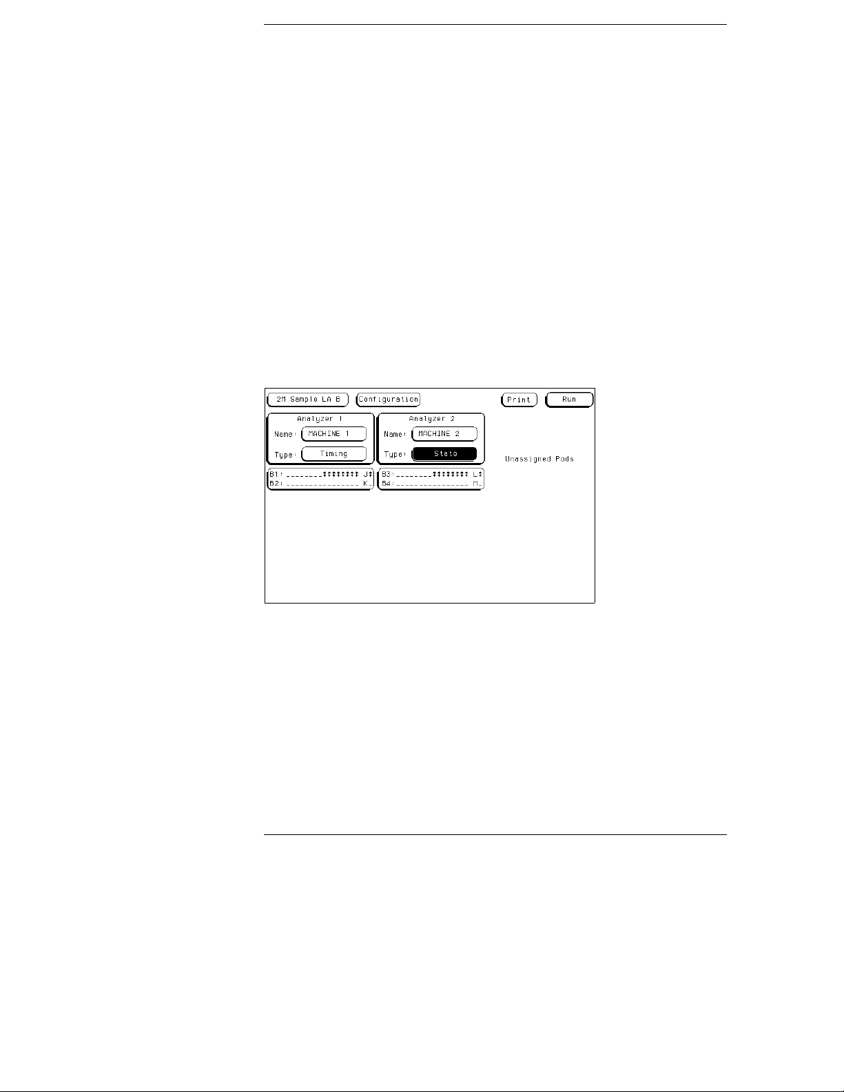
The Configuration menu allows you to set module level parameters.
You can partition the module into one or two independent analyzers.
You can also assign pods to either analyzer, select the type of clocking
needed (state or timing), and provide names for each analyzer.
The fields on this menu are:
• Analyzer Name Field
• Analyzer Type Field
• Pod Fields
• Activity Indicators
Configuration Menu
3–2

Name field
Keypad pop-up
appears when you
select the name
field.
The Configurat ion Menu
Analyzer Name Field
Analyzer Name Field
The Name field lets you assign a specific name to the analyzer machine. Use
the pop-up alphanumeric keypad to enter the name. When you have stored
several configurations to disk and later reload them, having assigned a
specific name to an analyzer can help identify the measurement setup.
Name Field
3–3

The Configuration Menu
Analyzer Type Field
Analyzer Type Field
The Type field allows you to configure each analyzer as either a state or
timing analyzer. When the Type field is selected, the following choices are
available.
Off
•
Timing
•
State
•
State Compare
•
SPA
•
Timing
When you select Timing, the analyzer uses its own internal clock to clock
measurement data into the acquisition memory. This clock is asynchronous
to the signals in the target system. When this option is selected, some fields
specific to external clocks will not appear in the analyzer menus.
You can configure the machine with only one timing analyzer. If you select
both analyzers as timing analyzers, the first will be turned off.
State
When you select State, the analyzer uses a clock from the system under test
to clock measurement data into acquisition memory. This clock is
synchronous with the signals in the target system. You can configure both
analyzers as state analyzers. State mode does not allow you to access the
Compare menu.
State Compare
When State Compare is selected, the Compare menu is available in the main
menu selection. For more details on Compare, see chapter 9, "The Compare
Menu." State Compare mode functions much like State mode, except that
total memory is reduced by one-fourth.
3–4

Type field
Type pop-up menu
The Configurat ion Menu
Analyzer Type Field
SPA
SPA stands for System Performance Analysis. It uses an external clock like a
state analyzer but measures overall system performance rather than
recording discrete activity. For more details, see Chapter 11.
Type Field
3–5

The Configuration Menu
Pod Fields
Pod Fields
The list of unassigned pods in the Configuration menu shows the available
pods for the module configuration. Pod grouping and assignment is by pod
pairs. When you want to assign a pod pair to an analyzer, touch the pod field.
From the assignment menu, select a destination for the pod pair. Use the
same procedure to reassign pod pairs that have previously been assigned to
an analyzer.
Pod field
Unassigned Po ds Display
3–6
Pod assignment
pop-up menu

The Configurat ion Menu
Pod Fields
When both analyzers are turned on, the pods of the master card cannot be
assigned to the same analyzer. If you attempt to assign them to the same
analyzer, you’ll get an error message when you try to exit the configuration
menu. The error message gives an explanation of the problem and provides
selection fields with options for reassigning one of the pod pairs.
Pod Reassignment Menu
3–7

The Configuration Menu
Activity Indicators
Activity Indicators
Within each pod pair you’ll notice activity indicators for each bit of each pod.
These indicators appear in two places. One is in the pod pair displays of this
Configuration menu. The other place is in the bit reference line in the
Format menu just above the pod bit numbers.
When the logic analyzer is properly connected to an active target system,
you’ll see either a high-level dash, a low-level dash, or a transitional arrow in
the Activity Indicator displays for each pod pair. These indicators are very
useful in showing proper probe connections and that the logic levels are as
expected.
See Also The "Bit Assignment Fields" in chapter 4, "The Format Menu," for more
information on the activity indicators.
Activity Indicators
3–8

4
The Format Menu

The Format Menu
Use the Format menu to select which data channels are measured and
to set up the clocking arrangement to capture valid data. It allows you
to group and label the data channels from the system under test to fit
your particular measurement. In addition, for your convenience in
recognizing bit groupings, you can specify symbols to represent them.
If the analyzer is configured as a state analyzer, there are master and
slave clocks, clock qualifiers, and a variable clock setup and hold to
further qualify what data is captured. In addition, you can set
individual pod clock threshold levels. The Format menu contains the
following fields:
• State Acquisition Mode Field (State, State Compare, and SPA only)
• Timing Acquisition Mode Field (Timing only)
• Data on Clocks Display
• Pod Field
• Pod Clock Field (State only)
• Master and Slave Clock Field (State only)
• Setup/Hold Field (State only)
• Symbols Field
• Label Assignment Field
• Rolling Labels and Pods Field
• Label Polarity Fields
• Bit Assignment Fields
• Pod Threshold Field
4–2

The Format Menu
State Acquisition Mode Field (State, State Compare, and SPA only)
State Acquisition Mode Field (State, State Compare,
and SPA only)
The State Acquisition Mode field identifies the speed and memory depth of
the acquisition mode. In four or five-card systems, speed is reduced to 100
MHz. In State Compare mode, some memory depth is used for information
needed to perform a comparison.
135 MHz [100 MHz]/2M State
The State Acquisition Mode uses both pods in a pod pair. If time or state tags
are turned on, the total memory is split between data acquisition storage and
time or state tag storage. To maintain the full 2M per channel depth, leave
one pod pair unassigned. State clock speed is 135 MHz [100 MHz for four or
five-card configurations].
Acquisition mode field
Acquisition Mode Field
4–3

The Format Menu
Timing Acquisition Mode Field (Timing only)
Timing Acquisition Mode Field (Timing only)
The Timing Acquisition Mode field displays the acquisition type, the channel
width, and sampling speed of the present acquisition mode. In timing
acquisition mode, the analyzer stores measurement data at each sampling
interval. Use the Timing Acquisition Mode field to access an acquisition mode
selection menu.
2M Sample Full Channel 250MHz
The total memory depth is 2M, with data being sampled and stored at most
every 4 ns.
4M Sample Half Channel 500MHz
The total memory depth is 4M, with data being sampled and stored at most
every 2 ns.
4–4

The Format Menu
Data on Clocks Display
Data on Clocks Display
This display shows the clock input channels available for the present
configuration. There are four clock input channels (J, K, L, and M) for each
card of a module, one for each pod. This display shows only the clock input
channels for those pods that are assigned in the present configuration.
A single-card module has four clock input channels, each of which may be
used as a state clock (when the machine is configured for state mode) or as a
data channel (in either state or timing modes). In a multi-card module, only
the four clock input channels connected to the Clock Master card of the
module are available for use as state clocks, but all of the clock input
channels of the module (there are four for each card in the module) may be
used as data channels. A clock input channel, when used as a data channel,
is treated as an ordinary data channel, except it cannot be included in a
Range resource.
In the display panel, the clock input channels of the Clock Master card are
grouped on the right, underneath the slot letter of the Clock Master card,
with the clock input channels of the other cards displayed to the left of those
of the Clock master card. If any clock input channel is used as a data
channel, that bit must be assigned. Activity indicators above the clock
identifier show signal activity on that clock input channel.
Data on Clocks
display
Data on Clocks Display
4–5

The Format Menu
Pod Field
Pod Field
The Pod field identifies which pod of a pod pair is affected by the settings of
the bit assignment field, pod threshold field, and pod clock fields. In the
full-channel modes, this field is simply an identifier and is not selectable.
However, in the half-channel mode, the Pod field turns dark, which means it
is selectable. In the half-channel mode, one pod of a pod pair is selectable
and all pod settings affect the selected pod.
Pod clock field
Pod field
Pod Field
4–6

The Format Menu
Pod Clock Field (State only)
Pod Clock Field (State only)
There is one Pod Clock field for each pod in the machine, and it is used to
indicate whether that pod’s data lines are to be strobed into memory by the
Master clock, Slave clock, or both, in the Demultiplex mode of operation.
When the Pod Clock field is selected, a clock menu appears with the
following choices:
Master
•
Slave
•
Demultiplex
•
The Master and Slave clock events are specified in the Master and Slave clock
fields. These clock functions are available only in a state analyzer.
See Also The "Master and Slave Clock Field" later in this chapter for information about
configuring a clocking arrangement.
Pod Clock Field
4–7

The Format Menu
Pod Clock Field (State only)
Master
This option specifies that data on all pods designated "Master Clock," in a
single analyzer, are strobed into memory when the status of the clock lines
matches the clocking arrangement specified under the Master Clock.
Slave
This option specifies that data on a pod designated "Slave Clock" is latched
when the status of the state clock inputs meets the requirements of the slave
clocking arrangement. Then, followed by a match of the master clock and
the master clock arrangement, the slave data is strobed into analyzer memory
along with the master data. If multiple slave clocks occur between master
clocks, only the data latched by the last slave clock prior to the master clock
is strobed into analyzer memory.
Analyzer Memory
latches on Master Clock
latches on
Slave Clock
Data on Master
Latching Slave Data
Slave Latch
Data on Slave
4–8

The Format Menu
Pod Clock Field (State only)
Demultiplex
The Demultiplex mode is used to store two different sets of data that occur at
different times on the same channels. In Demultiplex mode, only one pod of
the pod pair is used, and that pod is selectable. Both the master and slave
clocks are used in the Demultiplex mode. Channel assignments are displayed
as Demux Master and Demux Slave. For easy recognition of the two sets of
data, assign slave and master data to separate labels.
Demultiplex Clocking Mode
4–9

The Format Menu
Pod Clock Field (State only)
When the analyzer sees a match between the state clock inputs and the slave
clock specification, Demux Slave data is latched. Then, followed by a match
of the state clocks and the master clock specification, the slave data is
strobed into analyzer memory along with the master data. If multiple slave
clocks occur between master clocks, only the data latched by the last slave
clock prior to the master clock is strobed into analyzer memory.
Analyzer Memory
latches on Master Clock
latches on
Slave Clock
Same pod
Data on Master
Latching Slave Data in Demultiplex Mode
Slave Latch
Data on Slave
4–10

The Format Menu
Pod Threshold Field
Pod Threshold Field
Use the Pod Threshold field to set a voltage level the data must reach before
the analyzer recognizes and displays it as a change in logic levels. You specify
a threshold level for each pod. The level specified for each pod is also
assigned to the pod’s clock threshold. When the Pod Threshold field is
touched, a threshold selection pop-up menu appears with the following
choices:
TTL
When TTL is selected as the threshold level, the data signals must reach +1.5
volts.
ECL
When ECL is selected as the threshold level, the data signals must reach –1.3
volts.
Pod threshold field
Pod threshold pop-up
menu
USER
When USER is selected as the threshold level, the data signals must reach a
user selectable value between –6.0 volts to +6.0 volts.
Pod Threshold Field
4–11

The Format Menu
Master and Slave Clock Fields (State only)
Master and Slave Clock Fields (State only)
The Master and Slave Clock fields are used to construct a clocking
arrangement. A clocking arrangement is the assignment of appropriate
clocks, clock edges, and clock qualifier levels which allow the analyzer to
synchronize itself on valid data.
When the Master or Slave Clock field is selected, a clock/qualifier selection
menu appears showing the available clocks and qualifiers for a clocking
arrangement. There are four clocks available (J, K, L, M), and four clock
qualifiers available (Q1 through Q4).
A single-card module can use any of its four clocks as a state clock for
specifying Master and Slave clocking arrangements. For a multi-card module,
only the four clocks of the Clock Master board are available for use as state
clocks. Any unassigned clocks may be used as data channels.
See Also The "Pod Clock Field" earlier in this chapter for information on selecting
clocking arrangement types such as Master, Slave, or Demultiplex.
Master Clock Field
4–12
Master Clock field

The Format Menu
Master and Slave Clock Fields ( State only)
All combinations of the J and K clock and Q1 and Q2 qualifiers are ORed to
the clock combinations of the L and M clocks and Q3 and Q4 qualifiers. Clock
edges are ORed to clock edges, clock qualifiers are ANDed to clock edges,
and clock qualifiers can be either ANDed or ORed together. The clock
threshold level is the same as the level assigned in the Pod Threshold field.
Clock Edges and Levels
4–13

The Format Menu
Setup/Hold Field (State only)
Setup/Hold Field (State only)
Setup/Hold adjusts the relative position (in time) of the clock edge with
respect to the time period that data is valid. When the Setup/Hold field is
selected, a configuration menu appears. Use this Setup/Hold configuration
menu to select each pod in the analyzer and assign a Setup/Hold selection
from the selection list.
With a single clock edge assigned, the choices range from 3.0 ns Setup/0.0 ns
Hold to -0.5 ns Setup/3.5 ns Hold. With both edges of a single clock assigned,
the choices are from 3.5 ns Setup/0.0 ns Hold to -0.5 ns Setup/4.0 ns Hold. If
the analyzer has multiple clock edges assigned, the choices range from 4.0 ns
Setup/0.0 ns Hold to -0.5 ns Setup/4.5 ns Hold.
Setup and Hold Menu
4–14

The Format Menu
Setup/Hold Field (State only)
The relationship of the clock signal and valid data under the default setup
and hold is shown below.
Default Setup and Hold
If the relationship of the clock signal and valid data is such that the data is
valid for 1 ns before the clock occurs and 3 ns after the clock occurs, you
could use 1.0/2.0 or 0.5/2.5 or 0.0/3.0, but 0.5/2.5 would be the best choice.
Clock Position in Valid Data
4–15

The Format Menu
Symbols Field
Symbols Field
See Also Symbols Assignment in "Common Module Operations" in the HP 16500C
User’s Reference for complete information on using symbols.
Label Assignment Fields
See Also Labels Assignment in "Common Module Operations" in the HP 16500C
User’s Reference for complete information on using labels.
Rolling Labels and Pods
The rolling function is the same for all items that are stored offscreen.
See Also Labels Assignment in "Common Module Operations" in the HP 16500C
User’s Reference for complete information about rolling labels and pods.
4–16

The Format Menu
Label Polarity Fields
Label Polarity Fields
Use the Label Polarity fields to assign a polarity to each label. The default
polarity for all labels is positive ( + ). Change the label polarity by touching
the polarity field. This toggles between positive ( + ) and negative ( – )
polarity.
When the polarity is inverted, all data, as well as bit pattern specific
configurations used for identifying, triggering, or storing data, reflect the
change of polarity. In a timing analyzer with the data inverted, the waveform
display does not change.
Polarity field
Polarity Field
4–17

The Format Menu
Bit Assignment Fields
Bit Assignment Fields
The bit assignment fields are used to assign bits (channels) to labels. The
convention for bit assignment is as follows:
* (asterisk) indicates an assigned bit.
•
. (period) indicates an unassigned bit.
•
To change a bit assignment, select the bit assignment field and, using the
knob, move the cursor to the bit you want to change, then select an asterisk
or a period. When the bits are assigned as desired and you close the pop-up
menu, the screen displays the new bit assignment.
See Also "Activity Indicators" in chapter 3, "The Configuration Menu," for more
information on the bit reference line and the activity indicators on the bit
reference line.
Bit assignment field
Bit Assignment Field
4–18

The Format Menu
Bit Assignment Fields
Labels may have from 1 to 32 channels assigned to them. If you try to assign
more than 32 channels to a label, the logic analyzer will beep and a message
will appear at the top of the screen telling you that 32 channels per label is
the maximum. Channels assigned to a label are numbered from right to left,
with the least significant bit on the far right, numbered 0.
Although labels can contain split fields, assigned channels are always
numbered consecutively within a label.
Bit Assignment Example
4–19

4–20

5
The Trigger Menu

The Trigger Menu
The Trigger menu is used to specify when the analyzer triggers and
what the analyzer stores in acquisition memory. The Trigger menu
can be viewed as having four functionally different sections:
• Automatic Sequence Levels, located in the large light blue center
box
• Manual Sequence Levels, also located in the large light blue center
box
• Resource Terms, located at the bottom of the menu
• Control Fields, located at the right side of the display
The Trigger Menu
5–2

Predefined Trigger Macros
The state and timing acquisition modes each have a macro library
containing predefined trigger macros. Each macro will require at least
one sequence level, and in some cases, several levels. Macros can be
branched to by combining a user-defined level with a macro level. To
use these predefined trigger macros, see "Using Macros to Create a
Trigger Specification" on the next page. The macro libraries are as
follows:
Timing Trigger Macro Library:
• User Mode (user-defined macro)
• Basic Macros
• Pattern/Edge Combination Macros
• Time Violation Macros
• Delay Macros
State Trigger Macro Library:
• User Mode (user-defined macro)
• Basic Macros
• Sequence Dependent Macros
• Time Violation Macros
• Delay Macros
5–3

The Trigger Menu
Using Macros to Create a Trigge r Specification
1. From the Trigger menu, enter the desired sequence level by selecting the
Modify Trigger field or by selecting a sequence level number.
See Also "Modify Trigger Field" for information on accessing levels.
2. From within the sequence level, select the Select New Macro field
3. Scroll to highlight the macro you want, then select the Done field.
4. Select the appropriate assignment fields and insert the desired predefined
resource terms, numeric values, and other parameter fields required by the
macro. Select the Done field.
See Also "Resource Terms" for information on using predefined resource terms.
5–4

Timing Trigger Macro Library
The following list contains the macros in the Timing Trigger Macro Library.
They are listed in the order in which they appear on the screen.
User Mode User level - custom combinations, branching
The User level lets you manually design a sequence level. It uses one internal
sequence level.
Basic Macros 1. Find anystate n times
This macro becomes true with the nth state it sees. It uses one internal
sequence level.
2. Find pattern present/absent for > duration
This macro becomes true when it finds a pattern you have designated that
has been present or absent for greater than or equal to the set duration. It
uses one internal sequence level.
The Trigger Menu
Timing Trigger Macro Library
3. Find pattern present/absent for < duration
This macro becomes true when it finds a pattern you have designated that
has been present or absent for less than the set duration. It uses four or five
internal sequence levels.
4. Find edge
This macro becomes true when the edge you have designated is seen. It uses
one internal sequence level.
5. Find Nth occurrence of an edge
This macro becomes true when it finds the occurrence of an edge you have
designated. It uses one internal sequence level. The 500-MHz trigger
sequencer may not count edges captured closer than 2 ns apart.
5–5

The Trigger Menu
Timing Trigger Macro Library
Pattern/Edge
Combinations
Time Violations 1. Find 2 edges too close together
1. Find edge within a valid pattern
This macro becomes true when a selected edge type is seen within the time
window defined by a pattern you have designated. It uses one internal
sequence level.
2. Find pattern occurring too soon after edge
This macro becomes true when a pattern you have designated is seen
occurring within a set duration after a selected edge type is seen. It uses
three or four internal sequence levels.
3. Find pattern occurring too late after edge
This macro becomes true when one edge type you have selected occurs and,
for a designated period after that first edge is seen, a pattern is not seen. It
uses two internal sequence levels.
This macro becomes true when a second selected edge is seen occurring
within a period you have designated after the occurrence of a first selected
edge. It uses three or four internal sequence levels.
2. Find 2 edges too far apart
This macro becomes true when a second selected edge occurs beyond a
period you have designated after the first selected edge. It uses two internal
sequence levels.
3. Find width violations on a pattern/pulse
This macro becomes true when the width of a pattern violates minimum and
maximum width settings you have designated. It uses four or five internal
sequence levels.
Delay 1. Wait t sec
This macro becomes true after a period you have designated has expired. It
uses one internal sequence level.
5–6

State Trigger Macro Library
The following list contains the macros in the State Trigger Macro Library.
They are listed in the order in which they appear on the screen.
User Mode User Level - custom combinations, loops
The User level lets you manually design a sequence level. It uses one internal
sequence level.
Basic Macros 1. Find anystate n times
This macro becomes true with the nth state it sees. It uses one internal
sequence level.
2. Find event n times
This macro becomes true when it sees an event you have specified occurring
a designated number of times. The events may occur consecutively, but does
not have to. It uses one internal sequence level.
The Trigger Menu
State Trigger Macro Library
Sequence
Dependent Macros
3. Find event n consecutive times
This macro becomes true when it sees an event you have specified occurring
a designated number of consecutive times. It uses one internal sequence
level.
4. Find event2 immediately following event1
This macro becomes true when the first event you have specified is seen
immediately followed by a second designated event. It uses two internal
sequence levels.
1. Find event2 n times after event1, before event3 occurs
This macro becomes true when it first finds a designated event1, followed by
a selected number of occurrences of a designated event2. In addition, if a
designated event3 is seen anytime while the sequence is not yet true, the
sequence starts over. If event2’s nth occurrence is coincident with event3,
the sequence starts over. It uses two internal sequence levels.
5–7

The Trigger Menu
State Trigger Macro Library
2. Find too few states between event1 and event2
This macro becomes true when a designated event1 is seen, followed by a
designated event2, and with less than a selected number of states occurring
between the two events. It uses three or four internal sequence levels.
3. Find too many states between event1 and event2
This macro becomes true when a designated event1 is seen, followed by more
than a selected number of states, before a designated event2. It uses two
internal sequence levels.
4. Find n-bit serial pattern
This macro becomes true when a specified serial pattern of n bits is found.
Time Violations 1. Find event2 occurring too soon after event1
This macro becomes true when a designated event1 is seen, followed by a
designated event2, and with less than a selected period occurring between
the two events. It uses two internal sequence levels.
2. Find event2 occurring too late after event1
This macro becomes true when a designated event1 is seen, followed by at
least a selected period, before a designated event2 occurs. It uses two
internal sequence levels.
Delay 1. Wait n external clock states
This macro becomes true after a number of user clock states you have
designated has occurred. It uses one internal sequence level.
5–8

Sequence Levels
The Sequence Levels section controls when the analyzer triggers,
what the analyzer triggers on, and what data is stored in memory
before and after triggering occurs. By using sequence levels, you
create a sequence of instructions for the analyzer to follow. The
instructions contain user-defined resource terms representing such
things as timers, ranges, edges, and bit patterns.
As the resource terms are evaluated and acted upon by the analyzer,
all subsequent branching and storing within the sequence flow is
directed by your instructions. The path taken resembles a flow chart,
and the end result is the storage of only the data you need.
The state analyzer has 12 sequence levels available. The timing
analyzer has 10 sequence levels available.
5–9

The Trigger Menu
Sequence Level Number Field
Sequence Level Number Field
The Sequence Level Number field identifies an instruction to be evaluated by
the analyzer. In addition, use the number field to access the Sequence
Instruction menu, which allows you to define the automated trigger macros
and to manually construct sequence instructions.
The sequence instruction for each level is displayed in text and located just
to the right of the level number. The timer status in each level is also
displayed to the right of the instruction text.
Sequence Level Roll Field
The field rolls offscreen sequence levels back on screen by using the knob
when the Sequence Levels field is light blue. If the field is dark blue, select it,
turning it light blue.
Sequence Level Roll field
Sequence Level Number
field
Sequence Level Number
5–10

The Trigger Menu
Sequence Instruction Menu
Sequence Instruction Menu
When a Sequence Level Number field is selected, a Sequence Instruction
menu appears. Use this menu to create instructions for the Sequence Level
Number, to insert adjacent sequence levels, select a new macro, or to delete
the current level. The instruction you create will read like a sentence, with
the assigned resource terms directing how the analyzer qualifies and stores
the desired data. This Sequence Instruction Menu contains the following
fields to help you set up trigger conditions:
Insert Level and Delete Level Fields
•
Select New Macro field
•
Term assignment fields
•
Occurrence counter fields
•
Branching fields
•
Duration counter field (Timing only)
•
Timer Control field
•
Insert Level and Delete Level Fields
The Insert Level field is used to add another sequence level. When this field
is selected, depending on the analyzer configuration, you are given choices to
add a field before or after the current sequence level. A message appears
letting you know when all available sequence levels are inserted. The Delete
Level field is used to delete a selected sequence level.
See Also "Resource Term Fields" later in this chapter for information on assigning a
value to the Resource Terms.
Select New Macro Field
The Select New Macro field brings up a list of triggers that have been built
with predefined macros. There are separate libraries of predefined triggers
for State and Timing acquisition.
See Also "Predefined Trigger Macros" in this chapter for more information on
predefined trigger macros.
5–11

The Trigger Menu
Sequence Instruction Menu
Term Assignment Fields
The Term Assignment fields hold user-defined bit patterns, ranges, timers,
and logical combination resource terms. You can logically combine different
resource terms to form the kind of instruction needed to qualify the trigger
and store operations.
Occurrence Counter Field
The Occurrence Counter field indicates the number of times the analyzer
must see the resource term before it is allowed to advance to the next
sequence level. To assign an occurrence number, simply turn the knob, or
select the Occurrence Counter field and use the keypad that appears. The
maximum number of occurrences is 1048575. If the "Else on" term is seen
before all specified occurrences have taken place, the flow of the sequence
instruction goes to the sequence level designated in the Branching field.
See Also For information on selecting resource term choices and how to assign a value
to a resource term, refer to the term types, such as bit pattern, range, or
timers in this chapter.
Term assignment field
Occurrence Coun ter Field
5–12

The Trigger Menu
Sequence Instruction Menu
Branching Field
Each sequence level has two-way branching. If the first resource term is
found, the branch is to the next sequence level. If the first resource term is
not found, the analyzer evaluates the "Else on" secondary branching term.
If the "Else on" term is found, the secondary branch taken is to the
designated sequence level in the Branching field. If the "Else on" term is not
found, the analyzer continues to loop within the sequence level until one of
the two branches is found. If the "Else on" branch is taken, the occurrence
counter is reset even if the "go to level" branch is to the same level.
If both terms are found at the same time, the branch is to the next sequence
level after the required number of first term occurrences.
Branching across trigger levels is possible. If this occurs, the sequence level
evaluation could loop without ever seeing a trigger term. Take care in
designing your flowchart and constructing the sequence instructions to avoid
this possibility.
To set a sequence level branch, select the Branching field, then select a
destination sequence level number.
Branching in a Sequence Instruction
5–13

The Trigger Menu
Sequence Instruction Menu
Duration Counter Field (Timing only)
The Duration Counter field displays a user-definable period for which the
resource term must be valid before the analyzer continues with the sequence
evaluation.
> Field When the greater-than sign( >) precedes the Duration Counter field,
the analyzer continues sequence level evaluation only after the resource term
has been true for a period greater than or equal to the duration specified.
< Field When the less-than sign (<) precedes the Duration Counter field,
the analyzer continues sequence level evaluation only after the resource term
has been true for a period less than or equal to the duration specified. Each
less-than assignment (<) uses three sequence levels.
When < or > duration is assigned, the secondary branching (Else on) is not
available. To assign a duration, simply turn the knob, or select the Duration
Counter field and use the keypad that appears.
Occurs Field When "Occurs" is selected, the Duration Counter field
changes to an occurrence counter, and the sequence evaluation is delayed
until the resource term has occurred for the number of occurrences selected.
To assign an occurrence number, simply turn the knob, or select the
occurrence field and use the keypad that appears. The maximum number of
occurrences is 1048575.
5–14

The Trigger Menu
Sequence Instruction Menu
When the "Occurs" selection is made, the "Else on" resource term (secondary
branch) becomes available for a second branching option. If the first
resource term (primary branch) is not found, and the second resource term
is found, the analyzer branches to the sequence level designated in the
Branching field.
Sequence Level Instruction
5–15

The Trigger Menu
Sequence Instruction Menu
Timer Control Field
The Timer Control field is used to access the Timer Control menu. Use the
Timer Control menu to Start, Stop, Pause, or Continue timer operation as the
analyzer enters a sequence level. You can control the same timer from each
sequence level. The default timer condition in all sequence levels is Off.
Timer Control Menu
5–16

Resource Terms
Resource terms are the user-defined variables that you can place in
the Term Assignment fields of the sequence instructions. Resource
terms can take the form of bit patterns, ranges, timers, or edge terms.
They are used separately or in logical combinations with other terms.
The analyzer evaluates the sequence instruction and resource terms
and determines if the instruction is true or false. Depending on a true
or false evaluation, the appropriate branching direction occurs. The
terms and fields are:
• Resource Term Fields
• Bit Pattern Terms
• Range Terms
• Timer Terms
• Edge Terms (Timing only)
• Combination of Terms
5–17

The Trigger Menu
Resource Term Fields
Resource Term Fields
The Resource Term fields identify the terms available for use within the
analyzer. The Resource Term fields are also used to access the Resource
Term Configuration menu.
Just to the right of the Resource Term fields are the corresponding
assignment fields which display the assigned values and are also used to
access an assignment keypad.
Resource Terms Roll Field
Offscreen resource terms are rolled back onscreen by using the knob when
the Terms field is light blue. If the Terms field is dark blue, it must be
selected, which then turns it light blue.
Resource terms fields
Resource Term Fields
5–18

The Trigger Menu
Resource Term Fields
Resource Term Configuration Menu
When any of the Resource Term fields are selected, a Resource Terms
Configuration menu appears. Use this configuration menu to assign a
resource term to an analyzer, set the resource term to a value, or customize
the name of a resource term. The following functions can also be
accomplished by selecting the assignment field and using the pop-up keypad.
Clear (=X) Sets the Term Assignment fields as follows:
In Terms a – j, the assignment field is set to all Xs (don’t cares).
In Range 1 and 2 terms, the two assignment fields are set to maximum
(Fs) and minimum (0s) settings.
In Timer 1 and 2 terms, the assignment field is reset to a minimum
time of 400 ns.
In Edge 1 and 2 terms, the assignment field is reset to a period (.).
Set (=1) Sets the Term Assignment fields as follows:
In Terms a – j, the assignment field is set to all 1s (highs).
This option is not available for the two Range, Timer, and Edge terms.
Resource Terms Configur ation Menu
5–19

The Trigger Menu
Resource Term Fields
Reset (=0) Sets the assignment fields as follows:
In Terms a – j, the assignment field is set to all 0s (lows). This option
is not available for the two Range, Timer, and Edge terms.
Rename This function accesses a keypad that you use to create a custom
name for the resource term. This function works for all resource terms.
Assign All of the available resource terms except Edge terms can be
assigned to any analyzer. The Edge terms are only used in a timing analyzer.
A term, however, can be assigned to only one analyzer at a time. When a
resource term is selected, it toggles between analyzers.
Resource Term Assignment Menu
5–20

The Trigger Menu
Bit Pattern Terms
Bit Pattern Terms
Bit Pattern terms are set to match the numeric value or bit pattern of a group
of data channels. The ten available Bit Pattern terms are "a" through " j."
Each term can be assigned to either of the two analyzers, but not both. The
complement of the bit patterns you specify for "a" through "j" are available by
selecting "≠a" through "≠j."
Bit Pattern Assignment
The assignment of a bit pattern to the resource terms "a" through "j" can be
done in two ways. If you want a pattern of all 1s, all 0s, or all Xs (don’t cares),
you can insert these values by selecting the resource term field itself, then
select your choice from the Resource Term Configuration menu.
If you want some other pattern, use the pop-up keypad to assign the bit
pattern. The keypad becomes available when you select the assignment field
for each term.
Bit Pattern Resource Term
5–21

The Trigger Menu
Bit Pattern Terms
Bit Pattern Selection
After the resource terms have values assigned, they are inserted into the
sequence instruction where they direct the flow of that sequence instruction.
Insert Bit Pattern terms into a sequence instruction by selecting the Term
Assignment field, then selecting a term "a" through "j" from the pop-up
selection list.
Bit Pattern Term Selection
5–22

The Trigger Menu
Range Terms
Range Terms
Range terms bracket groups of bit patterns. There are two available Range
terms. Each Range term is assigned to either of the two analyzers, but not
both.
When you assign an upper and lower bit pattern boundary, the range is
recognized when the data is numerically between or on the two specified
boundaries. In addition, the range must be contained in a single pod pair,
with no clock bits allowed.
Range Assignment
To assign bit patterns to the upper and lower boundaries of a Range term,
you use a pop-up keypad. The keypad appears when you select the upper or
lower Range term assignment fields.
You can clear the range boundaries by setting them to all Xs (don’t cares) by
selecting the Range term field and selecting the Clear (=X) field from the
Resource Term Configuration menu. The Clear (=X) option places zeros and
Fs in the upper and lower boundaries respectively.
Range Term
5–23

The Trigger Menu
Range Terms
Range Term Selection
With upper and lower range boundaries assigned, insert the appropriate
In range or Out range terms into the sequence instruction. The In range term
is true when the analyzer recognizes a bit pattern on or between the assigned
range boundaries. The Out range term is true when the In range term is false.
In and Out range terms are inserted into a sequence instruction by selecting
the Term Assignment field, then selecting an "In range 1, 2" or "Out range 1,
2" term from the pop-up selection list.
Range Term Selection
5–24

The Trigger Menu
Timer Terms
Timer Terms
There are two available Timer terms, each of which may be assigned to either
of the two analyzers, but not both. Timers can be used as either the trigger
term, the store term, or a branching term, within a sequence level. With
timers inserted into sequence levels, you can start a timer in one level, pause
it, or stop it in another sequence level.
As with other resource terms, timers are either true or false. Timers start as
you enter the sequence level, and when its count expires, it becomes true. If
a timer is paused in one level, it must be continued in another level before it
can count through and become true. Timers can also be inverted, so a timer
can start as true and become false when its count expires.
Timer Assignment
To assign a time value to the Timer 1, 2 terms, you use a pop-up keypad
which appears when you select the assignment field.
Timer Term Assignment
5–25

The Trigger Menu
Timer Terms
The minimum value a timer can have is 400 ns, and that is the default value.
As more sequence levels are added, the timer status in the new levels
defaults to Off. Timers must be continued or started in each new level as is
appropriate. When a timer expires or stops, its count resets to zero.
Timer Term Selection
Timer terms are inserted into a sequence instruction by selecting the Term
Assignment field, then selecting a "Timer 1, 2" term from the pop-up
selection list.
Timer Term Selection
5–26
Timer term

The Trigger Menu
Edge Terms (Timing only)
Edge Terms (Timing only)
Edges and glitches can be used to qualify a trigger, store, or branch operation
within a sequence instruction. They can be used singularly or in combination
with each other across all assigned channels. When you specify an edge or
glitch on more than one channel, the analyzer ORs the edges and glitches. If
you want to qualify a glitch, place an asterisk (*) on the data channel you are
watching. If you want to qualify an edge, place the appropriate edge on the
data channel you are watching. The following edge choices are available:
Positive edge (↑)
Negative edge (↓)
Either positive or negative (↕)
No edge (.)
Edge Assignment
After you select the edge assignment field, an assignment menu appears. Use
the knob to position the cursor over the bit you want to qualify, then select
the glitch or edge choice.
Edge Term
5–27

The Trigger Menu
Edge Terms (Timing only)
When you finish assigning edges and glitches, select Done. After the
assignment menu closes, you will see "$" or "*" or both indicators in the
assignment field display. These symbols signify an assigned edge ($) or glitch
(*) qualifier. When Binary is selected for the numeric base, you see the
actual edge and glitch assignments.
Edge and Glitch Identifiers
5–28
 Loading...