


Errata
16550A Service Guide
16550-90901
April 1992
Title & Document Type:
Manual Part Number:
Revision Date:
HP References in this Manual
This manual may contain references to HP or Hewlett-Packard. Please note that HewlettPackard's former test and measurement, semiconductor products and chemical analysis
businesses are now part of Agilent Technologies. We have made no changes to this
manual copy. The HP XXXX referred to in this document is now the Agilent XXXX.
For example, model number HP8648A is now model number Agilent 8648A.
About this Manual
We’ve added this manual to the Agilent website in an effort to help you support your
product. This manual provides the best information we could find. It may be incomplete
or contain dated information, and the scan quality may not be idea l. If we find a better
copy in the future, we will add it to the Agilent website.
Support for Your Product
Agilent no longer sells or supports this product. You will find any other available
product information on the Agilent Test & Measurement website:
www.tm.agilent.com
Search for the model number of this product, and the resulting product page will guide
you to any available information. Our service centers may be able to perform calibration
if no repair parts are needed, but no other support from Agilent is available.

Service Guide
Publication number 16550- 90901
First edition, April 1992
HP 16 550A
100-MHz State/500-MHz Timing
Logic Analyzer

HP 16550A 100-MHz State/500-MHz Timing Logic Analy ze r
The HP 16550A is a 100-MHz State/500-MHz Timing Logic Analy zer mod ule for
the HP 16500A Logic Analys is Syst em. The HP 16550A offers hig h perf orma nce
measurement capabilit y.
Featu res
Some of the main features of the HP 16550A are as follows:
• 96 data channe l s
• 6 clock/data channels
• 4K memory depth per channel
• 100 MHz maximum state acquisition speed
• 500 MHz maximum timing acquisition speed
• Expandable to 204 ch an nels
Service Strateg y
The service strategy for this ins trument is the replaceme nt of defectiv e assemblies.
This service guide contains inf ormation for finding a defective assembly by testing
and servicing the HP 16550A st ate and timin g analyz er module.
This module can be return ed to Hewlett -Pac kard for all service work, inc lud ing
troublesh ootin g. Conta ct your neares t Hewle tt -P ac kard Sale s Off ice for more
details.
iv

The HP 16550A 100-MHz State/500-MHz Timing Logic Analyzer
v

In This Book
This book is the service guide for the HP 16550A 100-MHz State/500-MHz Timing Logic
Analyzer module. Place this service guide in the 3-ring binder supplied with your
16500A Logic Analysis System Service Manual
This service guide is divided into eight chapters.
Chapter 1 contains information about the module and includes accessories for the module,
specifications and characteristics of the module, and a list of the equipment required for
servicing the module.
Chapter 2 tells how to prepare the module for use.
Chapter 3 gives instructions on how to test the performance of the module.
Chapter 4 contains calibration instructions for the module.
Chapter 5 contains self-tests and flowcharts for troubleshooting the module.
Chapter 6 tells how to replace the module and assemblies of the module and how to return
them to Hewlett-Packard.
Chapter 7 lists replaceable parts, shows an exploded view, and gives ordering information.
Chapter 8 explains how the analyzer works and what the self-tests are checking.
.
HP
vi

Contents
1 General Information
Accessories 1–2
Specifications 1–3
Characteristics 1–4
Supplemental Characteristics 1–5
Recommended Test Equipment 1–8
2 Preparing for Use
To inspect the module 2–2
To prepare the ma inframe 2–3
To configure a one-car d module 2–4
To configure a two-card module 2–5
To install the module 2–6
To turn on the system 2–7
To test the module 2–7
3 Testing Performance
To perform the self-tests and make the test connectors 3–3
To test the threshold accuracy 3–7
To test the glitch capture 3–16
To test the single-clock, single-edge, state acquisition 3–22
To test the multiple-clock, multiple-edge, state acquisition 3–35
To test the single-clock, multiple-edge, state acquisition 3–48
To test the time interval accuracy 3–60
To perform the two-card test 3–66
Performance Test Record 3–77
4 Calibrating
5 Troubleshooting
To use the flowcharts 5–2
To run the self-tests 5–8
To test the cables 5–12
To test the auxiliary power 5–16
vii

Contents
6 Rep la cing Assemblies
To remove the module 6–2
To replace the circuit board 6–3
To replace the module 6–4
To replace the probe cable 6–6
To return assemblies 6–6
7 Rep laceable Parts
Replaceable Parts Ordering 7–2
Replaceable Parts List 7–3
Exploded View 7–5
8 Theory of Operation
Block-Level Theory 8–2
Self-Tests Description 8–7
viii

1
Accessories 1–2
Specifications 1–3
Characteristics 1–4
Supplemental Cha ract erist ics 1–5
Recommended Test Equipment 1–8
General Information

General Information
This chapter lists th e acces sorie s, th e specif ications and characteristics , and the
recommended te st equipme nt.
Accessories
The following accessories are supplied with the HP 16550A logic analyzer.
Accessories Supplied HP Part Number
Probe Tip Assembly, Qty 6 01650-61608
Grabbers, Qty 6 packages 5090-4356
Extra Probe Leads, Qty 1 package 5959-9333
Probe Cable ID Clip, Qty 1 16500-41201
Probe Cables, Qty 3 16550-61601
Probe Cable and Pod Labels, Qty 1 01650-94310
Accessories Available
The accessories available for the HP 16550A are listed in the
Analyzers
brochure.
Accessories for HP Logic
1–2

General Information
Specifications
Specifications
The specifications are the performance standards against which the product is tested.
Maximum State Speed 100 MHz
Minimum State Clock Pulse Width
Minimum Master to Master Clock Time
Minimum Glitch Width 3.5 ns
Threshold Accuracy ± (100 mV + 3% of threshold setting)
Setup/Hold Time:
*
Single Clock, Single Edge 0.0/3.5 ns through 3.5/0.0 ns,
Single Clock, Multiple Edges 0.0/4.0 ns through 4.0/0.0 ns,
Multiple Clocks, Multiple Edges 0.0/4.5 ns through 4.5/0.0 ns,
*
*
3.5 ns
10.0 ns
adjustable in 500-ps increments
adjustable in 500-ps increments
adjustable in 500-ps increments
*
Specified for an input signal VH = −0.9 V, VL = −1.7 V, slew rate = 1 V/ns, and threshold = −1.3 V.
1–3

General Information
Characteristics
Characteristics
The characteristics are not specifications, but are inc luded as additional information.
Full Channel Half Channel
Maximum State Clock Rate 100 MHz 100 MHz
Maximum Conventional Timing Rate 250 MHz 500 MHz
Maximum Transitional Timing Rate 125 MHz 250 MHz
Maximum Timing with Glitch Rate N/A 125 MHz
Channel Count
Memory Depth 4K 8K
*
Channel count is doubled when two HP 16550A cards are connected together.
**For all modes except glitch.
*
102/204 51/102
**
1–4

General Information
Supplemental Characteristics
Supplemental Characteristics
Probes
Input Resistance 100 kΩ, ± 2%
Input Capatiance ~ 8 pF
Minimum Voltage Swing 500 mV, peak-to-peak
Threshold Range ± 6.0 V, adjustable in 50-mV increments
State Analysis
State/Clock Qualifiers 6
Time Tag Resolution
Maximum Time Count Between States 34 seconds
Maximum State Tag Count
Timing Analysis
Sample Period Accuracy 0.01 % of sample period
Channel-to-Channel Skew 2 ns, typical
Time Interval Accuracy ± [sample period + channel-to-channel skew
*
*
8 ns
4.29 x 10
9
+(0.01%)(time reading)]
Triggering
Sequencer Speed 125 MHz, maximum
State Sequence Levels 12
Timing Sequence Levels 10
Maximum Occurrence Counter Value 1,048,575
Pattern Recognizers 10
Maximum Pattern Width 102 channels in a one-card configuration.
204 channels in a two-card configuration.
Range Recognizers 2
Range Width 32 bits each
Timers 2
Timer Value Range 400 ns to 500 seconds
Glitch/Edge Recognizers 2 (timing only)
Maximum Glitch/Edge Width 102 channels in a one-card configuration.
204 channels in a two-card configuration.
*
Maximum state clock rate with time or state tags on is 100 MHz. When all pods are assigned to a state or timing machine, time or
state tags halve the memory depth.
1–5

General Information
Supplemental Characteristics
Measurement and Display Functions
Arming Each module can be armed by the RUN key, by the external PORT IN, or by
another module via the Intermodule Bus (IMB).
Displayed Wavefo rms 24 lines maximum, with scrolling across 96 waveforms.
Measurement Functions
Run/Stop Functions Run Starts acquisition of data in specified trace mode.
Stop In single trace mode or the first run of a repetitive acquisition, STOP halts
acquisition and displays the current acquisition data. For subsequent runs in repetitive
mode, STOP halts acquisition of data and does not change the current display.
Trace Mode Single mode acquires data once per trace specification. Repetitive mode
repeats single mode acquisitions until stop is pressed or until the time interval between
two specified patterns is less than or greater than a specified value, or within or not
within a specified range.
Indicators
Activity Indicators Provided in the Configuration and Format menus for identifying
high, low, or changing states on the inputs.
Markers Two markers (X and 0) are shown as dashed lines on the display.
Trigger Displayed as a vertical dashed line in the Timing Waveform display and as
line 0 in the State Listing display.
Data Entry/Display
Labels Channels may be grouped together and given a 6-character name. Up to
126 labels in each analyzer may be assigned with up to 32 channels per label.
Display Mod es State listing, State Waveforms, Chart, Compare Listing, Compare
Difference Listing, Timing Waveforms , and Timing Listings. State Listing, Timing
Waveforms and Oscilloscope Waveforms can be time-correlated on the same displays.
Timing Waveform Pattern readout of timing waveforms at X or 0 marker.
Bases Binary, Octal, Decimal, Hexadecimal, ASCII (display only), Two’s Complement,
and User-defined symbols.
Symbols 1,000 maximum. Symbols can be downloaded over RS-232 or HP-IB.
1–6

General Information
Supplemental Characteristics
Marker Functions
Time Interval The X and 0 markers measure the time interval between one point on a
timing waveform and trigger, two points on the same timing waveform, two points on
different waveforms, or two states (time tagging on).
Delta States (state analyzer only) The X and 0 markers measure the number of
tagged states between one state and trigger or between two states.
Patterns The X and 0 markers can be used to locate the
pattern from trigger, or from the beginning of data. The 0 marker can also find the
occurrence of a pattern from the X marker.
Statistics X and 0 marker statistics are calculated for repetitive acqu isitions. Patterns
must be specified for both markers and statistics are kept only when both patterns can
be found in an acquisition. Statistics are minimum X to 0 time, maximum X to 0 time,
average X to 0 time, and ratio of valid runs to total runs.
Auxiliary Power
Power Thro u gh Cables 1/3 amp at 5 V maximum per cable
Operating Environ ment
Temperature Instrument, 0 °C to 55 °C (+32 °F to 131 °F).
Probe lead sets and cables,
0 °C to 65 °C (+32 °F to 149 °F).
Humidity Instrument, probe lead sets, and cables, up to
95% relative humidity at +40 °C (+122 °F).
Altitude To 4600 m (15,000 ft).
Vibration Operating: Random vibration 5 to 500 Hz,
10 minutes per axis, ≈0.3 g (rms).
Non-operating: Random vibration 5 to 500 Hz,
10 minutes per axis , ≈ 2.41 g (rms) ;
and swept sine resonant search, 5 to 500 Hz,
0.75 g (0-peak), 5 minute resonant dwell
at 4 resonances per axis.
nth
occurrence of a specified
nth
1–7

General Information
Recommended Test Equipment
Recommended Test Equipment
Equipment Required
Equipment Critical Specifications Recommended
Model/Part
Pulse Generator 100 MHz, 3.5 ns pulse width,
HP 8131A Option 020 P,T
< 600 ps rise time
Digitizing Oscilloscope
Function Generator
≥ 6 GHz bandwidth, < 58 ps rise time
Accuracy ≤(5)(10
−6
) × frequency,
HP 54121T P
HP 3325B Option 002 P
DC offset voltage ±6.3 V
Digital Multimete r 0.1 mV resolution, 0.005 % accuracy HP 3458A P
BNC-Banana Cable HP 11001-60001 P
BNC Tee BNC (m)(f)(f) HP 1250-0781 P
Cable BNC (m-m) 48 inch HP 10503A P
SMA Coax Cable (Qty 3)
≥ 18 GHz bandw idth
HP 8120-4948 P
Adapter (Qty 4) SMA(m)-BNC(f) HP 1250-1200 P
Adapter SMA(f)-BNC(m) HP 1250-2015 P
Coupler BNC (m-m) HP 1250-0216 P
20:1 Probes (Qty 2) HP 54600A P
BNC Test Connector,
17x2 (Qty 1)
BNC Test Connector,
6x2 (Qty 4)
**
**
Use
P
P,T
*
*
A = Adjustment P = Performance Tests T = Troubleshooting
**
Instructions for making these test connectors are in chapter 3, "Testing Performance."
1–8

2
To inspect the module 2–2
To prepare the mainframe 2–3
To configu re a one-ca rd module 2–4
To configu re a two -c ard mod ule 2–5
To install the module 2–6
To turn o n the system 2–7
To test the module 2–7
Preparing for Use

Preparing For Use
This chapter gives you instructions for preparing the logic analyzer module for use.
Power Requirements
All power supplie s required for operating the logic analy zer are su pp lied throu gh
the backplan e conn ect or in th e main frame .
Operatin g Environment
The operating environment is listed in chapter 1. Note the non-condensing
humidity limitatio n. Condensatio n with in the ins trume nt can cause poor operat ion
or malfunctio n. Provide prot ect ion agains t internal condensatio n.
The logic analyze r module will ope rate at all specif ica tio ns with in th e tempe rat ure
and humidity range given in chapte r 1. However, reliability is enhanced when
operatin g the mod ule within the following ranges:
• Temperature: +20 °C to +35 °C (+68 °F to +95 °F)
• Humidity: 20% to 80% non-condensing
Storage
Store or ship the logic analyze r in enviro nme nts within the follo wing limit s:
• Temperature: -40 °C to + 75 °C
• Humidity: Up to 90% at 65 °C
• Altitude : Up to 15,30 0 met ers (50 ,0 00 feet )
Protect the mod ule from tempe ratu re ext reme s which cause con dens ation on the
instrument.
To inspect the module
1 Inspect the shipping container f or dama ge .
If the shipping container or cushioning material is damaged, keep them until you have
checked the contents of the shipment and checked the instrument mechanically and
electrically.
2
Check the supp lied acce sso ries.
Accessories supplied with the module are listed in chapter 1, "Accessories Supplied."
3 Inspect the product for physical damage.
Check the module and the supplied accessories for obvious physical or mechanical defects.
If you find any defects, contact your nearest Hewlett-Packard Sales Office. Arrangements
for repair or replacement are made, at Hewlett-Packard’s option, without waiting for a claim
settlement.
2–2
To prepare the mainframe
Preparing for Use
To prepare the mainframe
CAUTION
CAUTION
Turn off the mainframe power before removing, replacing, or installing the module.
Electrostatic discharge can damage electronic component s. Use grounded wriststraps and
mats when performing any service to this module.
1
Turn off the mainframe power swit ch, then unplug the power cord . Disconne ct any
input or output connections.
2 Plan your module configuration.
If you are installing a one-card module, use any available slot in the mainframe.
If you are installing a two-card module, use two adjacent slots in the mainframe. The
bottom card will be the master card of the module. Up to two, two- card modules can be
installed in a mainframe.
3
Loosen the thumb screws.
Cards or filler panels below the slots intended for installation do not have to be removed.
Starting from the top, loosen the thumb screws on filler panels and cards that need to be
moved.
CAUTION
CAUTION
4
Starting from the top, pull the cards and filler panels that n eed to be moved halfway
out.
All multicard modules will be cabled together. Pull these cards out together.
Remove the cards and filler panels.
5
Remove the cards or filler panels that are in the slots intended for the module installation.
Push all other cards into the card cage, but not completely in. This is to get them out of the
way for installing the module.
Some modules for the Logic Analysis System require calibration if you move them to a
different slot. For calibration information, refer to the manuals for the individual modules.
2–3
CAUTION
Preparing for Use
To configure a one-card module
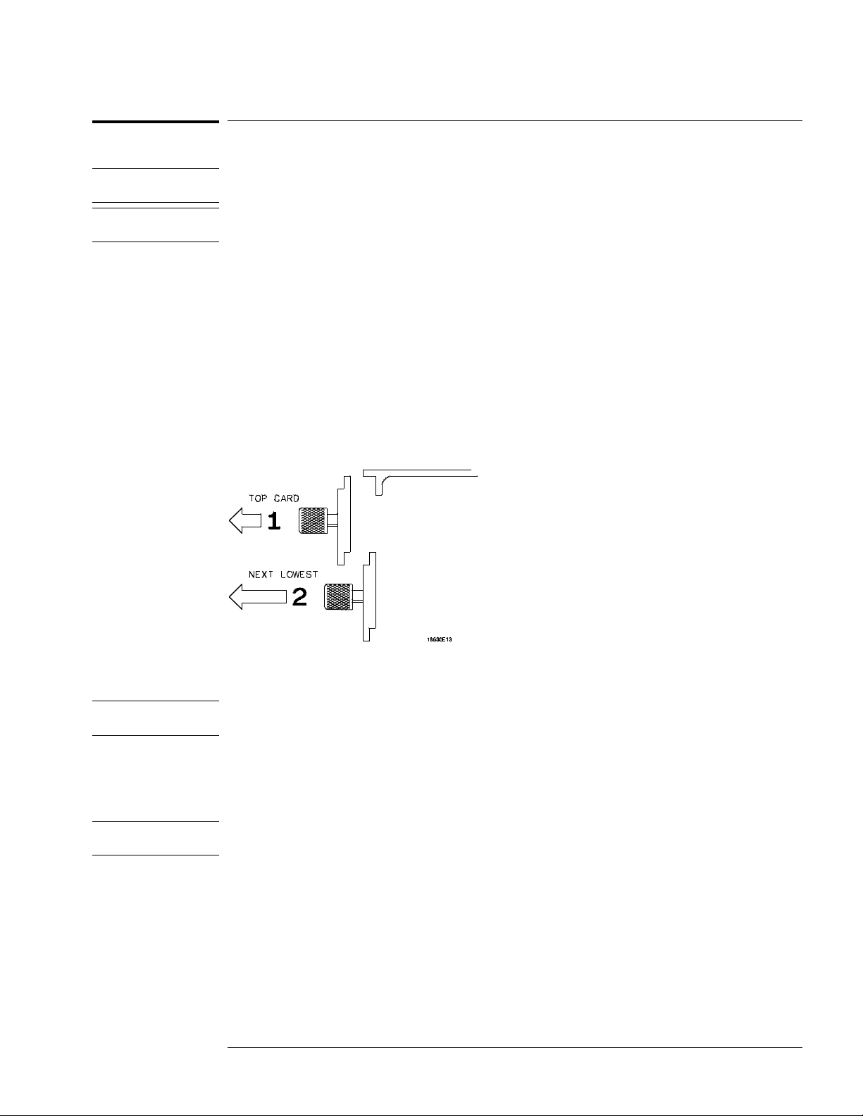
To configure a one-card module
• When shipp ed sepa rat ely, the module is con fig ured as a one-card mod ule . The
cables should be connected as sho wn in the figure.
• To configu re a two -c ard mod ule into a one-card modu le, remove the cable s
connecting the two cards, then co nnect th e ca ble s as sho wn.
If you pull on the flexible ribbon part of the cable, you might damage the cable assembly.
To remove a cable from the cable connector on the board, gently pry the hard plastic part of
the cable assembly away from the connector using a screwdriver.
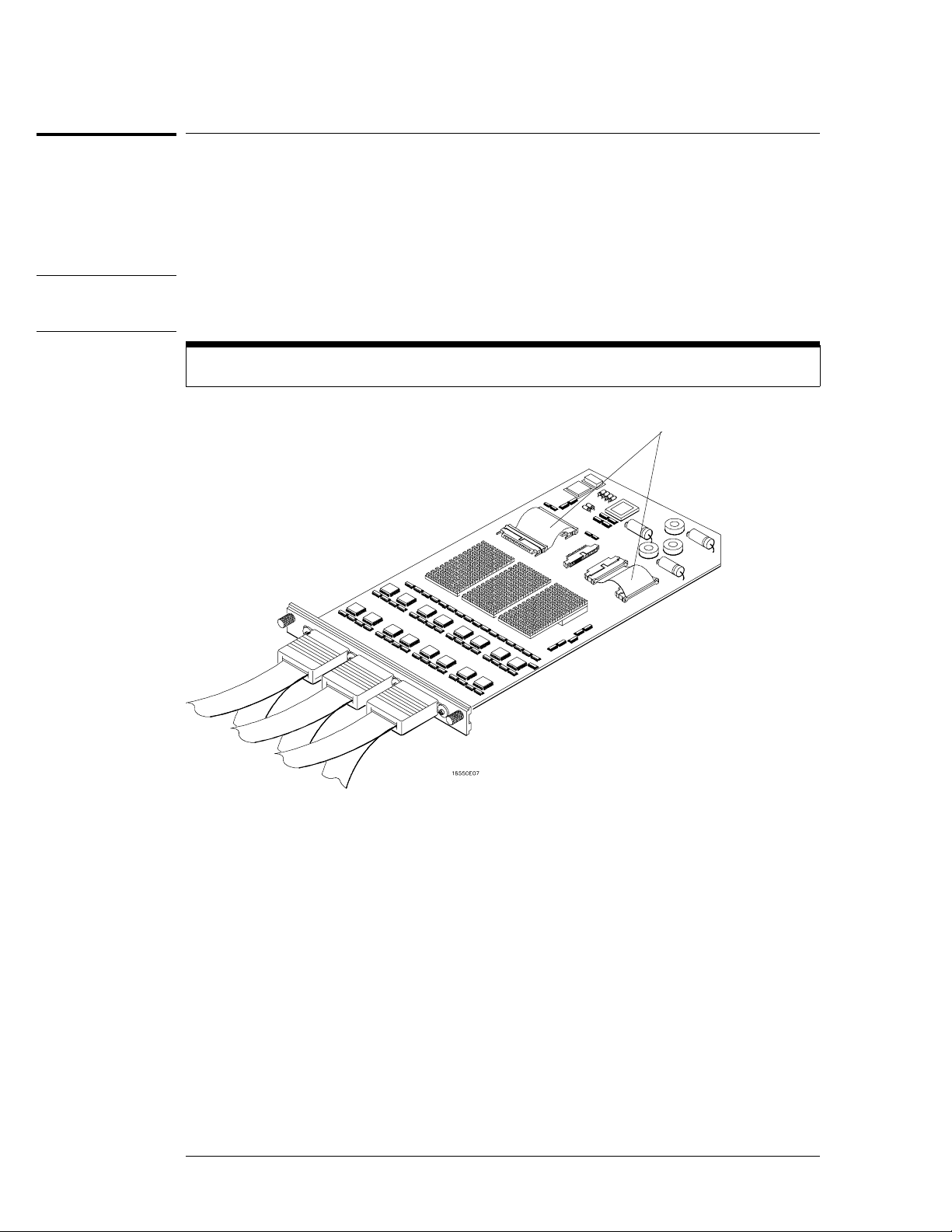
Directions for connecting the cables are printed on the circuit board.
Cables
2–4

CAUTION
Preparing for Use
To configure a two-card module
To configure a two-card module
Directions for connecting the cables are printed on the circuit board.
To configure a two-card module, connect the cables as follows.
1
Disconnect th e two cable s from J4 and J5 and from J7 and J8 on the card to go in
the upper slot.
If you pull on the flexible ribbon part of the cable, you might damage the cable assembly.
To remove a cable from the cable connector on the board, gently pry the hard plastic part of
the cable assembly away from the connector using a screwdriver.
2
Disconnect th e cable fro m J7 and J8 of the card to go in the lower slo t.
3 Connect the 80-pin cab le from J6 of the lowe r card to J5 of the upper ca rd. The
cable between J4 and J5 of the lowe r card should remain connected.
4 Connect the 100-p in ca ble from J7 of the lower card to J7 of the upper card.
Save unused cables for future configurations.
2–5
Preparing for Use
To install the module
To install the module
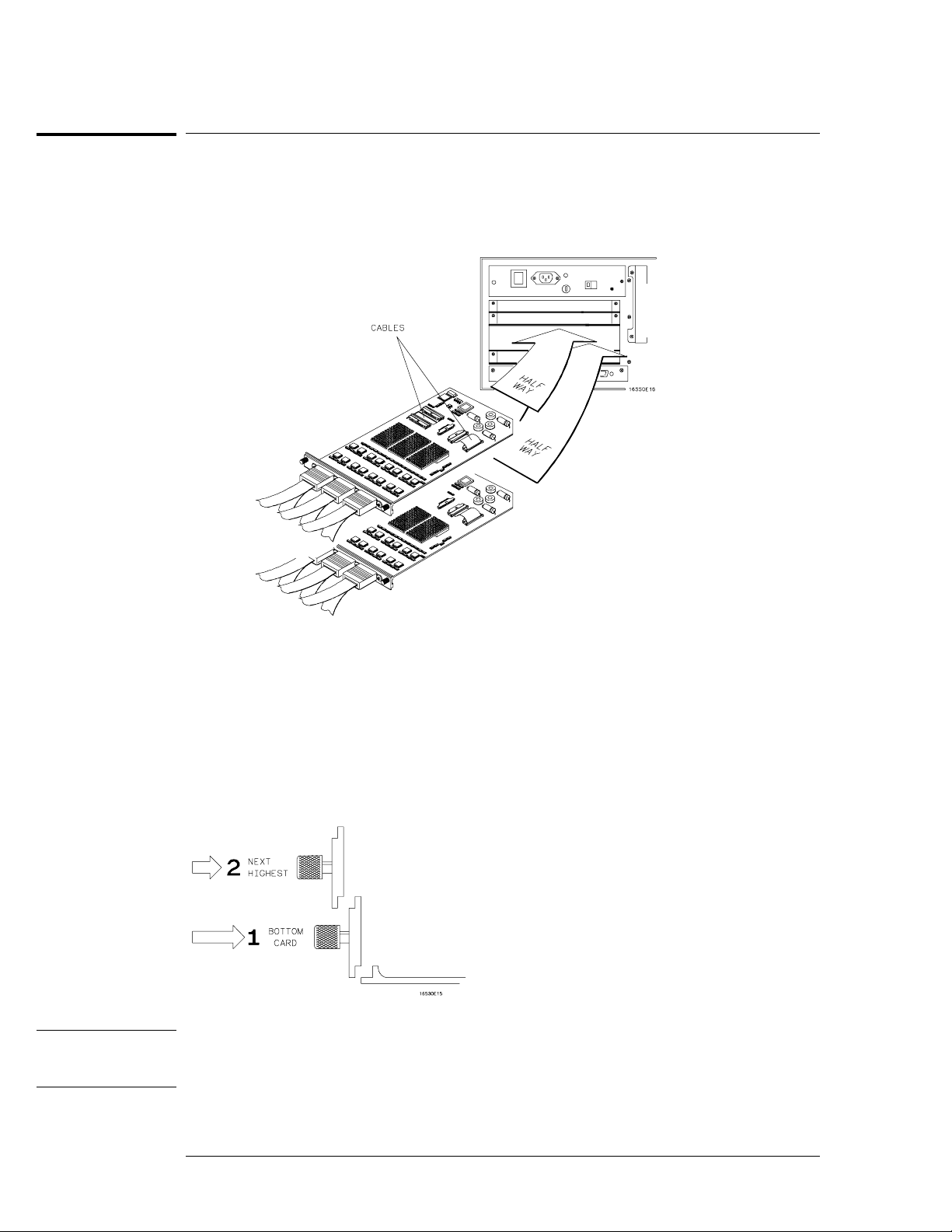
1 Slide the cards above the slot s for the mod ule about half way out of the mainf rame.
2 With the probe cables facin g awa y from the ins trume nt , slid e the module
approximately halfway into the main fra me.
CAUTION
3 Slide the complete module int o the main frame , but not co mple tely in.
Each card in the instrument is firmly seated and tightened one at a time in step 5.
4 Position all cards and filler pan els so that the endp lat es ov erlap .
5 Seat the cards and tighten t he thumbscrews.
Starting with the bottom card, firmly seat the cards into the backplane connector of the
mainframe. Keep applying pressure to the center of the card endplate while tightening the
thumbscrews finger-tight. Repeat this for all cards and filler panels starting at the bottom
and moving to the top.
Correct air circulation keeps the instrument from overheating. For correct air circulation,
filler panels must be installed in all unused card slots. Keep any extra filler panels for future
use.
2–6

Preparing for Use
To turn on the system
To turn on the system
1 Connect the power cable to the mainframe.
2 Insert the disk containing the operating system a disk drive.
3 Turn on the instrument power switch.
When you turn on the instrument power switch, the instrument perfor ms powerup tests that
check mainframe circuitry. After the powerup tests are complete, the screen will look similar
to the sample screen below.
To test the module
The logic analyzer module does not require calibration or adjustment. After installing the
module, you can test and use the module.
• If you require a test to ve rif y the spe cif icat ion s, start at the beginning of chapter 3,
"Testing Perfo rmanc e. "
• If you require a test to initially accept the operation, perform the self-tests in
chapter 3.
• I f the module does not operate correctly, go to the beginning of chapter 5,
"Troubleshooting."
2–7

3
To perform the self-t est s an d make the test conne ct ors 3–3
To test the threshold accuracy 3–7
To test the glitch capture 3–16
To test the single-clock, single-edge, state ac quisition 3–22
To test the multiple-clock, multiple-edge, state acquisition 3–35
To test the single-clock, multiple-edg e, state acquisition 3–48
To test the time interval accuracy 3–60
To perform the two-card test 3–66
Performanc e Tes t Reco rd 3–77
Testing Performance

Testing Performance
This chapter t ells you how to test the performan ce of the logic analyzer again st the
specifica tio ns list ed in chapte r 1. To ensure the log ic analyz er is opera tin g as
specified , soft ware te st s (self-t est s) and manu al perfo rma nc e tests are done on the
module. The logic an aly zer is conside red performance-ve rified if all of the software
tests and manual performance tests have passed. The procedures in this chapter
indicate what constit utes a "Pass" sta tus for each of the tests.
Test St rategy
For a complete test , st art at the beginn ing with the software te st s and con tin ue
through to the end of the chapte r. For an ind ividu al te st , follow th e proc edure in th e
test.
One-card module
To perform a complete test on a one-card module, start at the beginning of the
chapter and follow each procedure.
Two-card module
To perform a complete test on a two-card module, perform th e software tests with
the cards connect ed . Then, remove th e two-card module from the mainfra me an d
configure each card as a one-card module. Install the one-card mod ules into the
mainframe and perf orm the one-card manual perfo rmanc e tests on each ca rd.
When the test s are comp let e, remove the one-card modu les, recon fig ure the m into
two-card modules, reinstall them int o th e mainfra me, the n perform th e final
two-card test . For remova l inst ruct ion s, se e chapt er 6, "Replac ing Asse mblie s."
For installation and configuration instructions, see chapter 2, "Preparing for Use."
Test Interval
Test the performa nce of the module at two-year inte rvals or if it is replace d or
repaired.
Test Record Descrip ti on
A performance te st reco rd for reco rdin g the resu lts of each proc edure is loca te d at
the end of this chapter. Use the perf orman ce test record to gauge the perf orma nce
of the module over time.
Test Equipment
Each procedu re lists th e reco mmen ded te st equipme nt . You can use equip ment
that satisfie s the specifications given. However, the procedu res are based on using
the recommende d mod el or part number.
Instrument Warm-Up
Before testin g the perfo rmanc e of the module, warm-u p the instrume nt and the test
equipmen t for 3 0 minute s.
3–2
To perform the self-t es t s and make t he test connect ors
The self-tests verify the correct opera tion of the logic analyzer mod ule . Self-tests
can be performed all at once or on e at a time. While test ing the perf orman ce of the
module, run the self-test all at once.
The test conn ect ors co nn ect the analyze r to th e test eq uip men t.
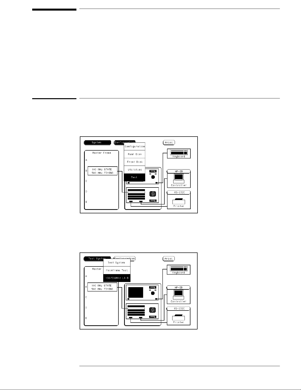
Perform the self-tests
1 Disconnect all input s, ins ert th e disk con tainin g th e operat ing syst em int o a disk
drive, then turn on the power switch .
2 In the System Co nf igu rat ion menu, to uch Conf igu ration. In the pop-up, touch Test.
3 Remove the disk containin g the opera ting system, then ins ert th e disk con ta inin g
the performance verif icat ion (self-t est s) into the disk drive . Touch the box lab eled
Touch box to Load Test System.
4 On the test system scre en , touch Test System. Select the 100 MHz/500 MHz LA
module to be tested.
3–3
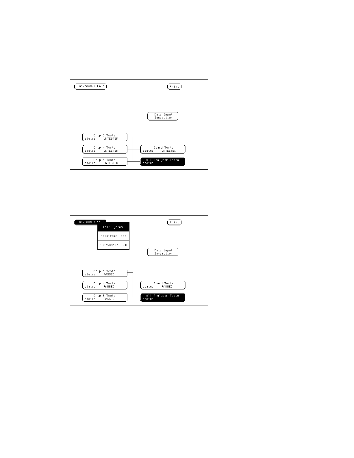
Testing Performance
To perform the self-tests and make the test connectors
5 Touch All An alyzer Tests.
You can run all tests at one time by touching All Analyzer Tests. To see more details about
each test when troubleshooting failures, you can run each test individually. This example
shows how to run all tests at once.
6
When the tests finis h, the stat us will show Passed or Failed. Reco rd the result s of
the test on the performa nce tes t reco rd at the end of this chapte r.
7 Touch 100/500 MHz LA. If more logic analyze r ca rds are to be test ed, sele ct the
next card, then repeat the tes t. When all cards are teste d, touch 100/500 MHz,
then select Test System.
8 Touch Configu ration, then select Exit Test . Remove the disk containing the
performanc e verif icat ion tes t, then inse rt th e disk cont ain ing the operat ing syste m.
Touch the box labeled Touch box to Exit Test System.
3–4
Testing Performance
To perform the self-tests and make the test connectors
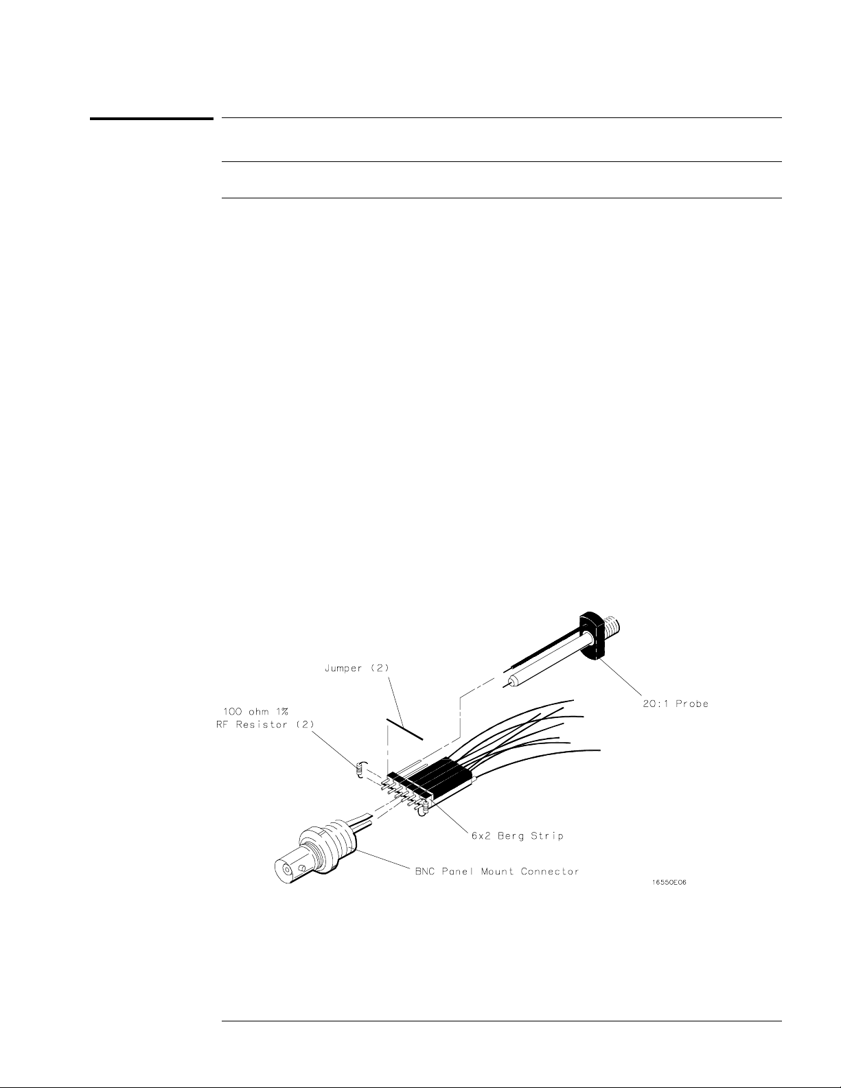
Make the test connectors
Materials Required
Description Recommended Part Qty
BNC (f) Connector HP 1250-1032 5
100 Ω 1% resistor
Berg Strip, 17 -by-2 1
Berg Strip, 6-by-2 4
20:1 Probe HP 54006A 2
Jumper wire
HP 0698-7212 8
1 Build four test connect ors us ing BNC connec to rs and 6-by-2 se ctio ns of Berg strip.
a Solder a jumper wire to all pins on one side of the Berg strip.
b Solder a jumper wire to all pins on the other side of the Berg strip.
c Solder two resistors to the Berg strip, one at each end between the end pins.
d Solder the center of the BNC connector to the center pin of one row on the Berg strip.
e Solder the ground tab of the BNC connector to the center pin of the other row on the
Berg strip.
f On two of the test connectors, solder a 20:1 probe. The probe ground goes to the
same row of pins on the test connector as the BNC ground tab.
3–5

Testing Performance
To perform the self-tests and make the test connectors
2 Build one test connector using a BNC connecto r and a 17-by-2 sect ion of Berg strip.
a Solder a jumper wire to all pins on one side of the Berg strip.
b Solder a jumper wire to all pins on the other side of the Berg strip.
c Solder the center of the BNC connector to the center pin of one row on the Berg strip.
d Solder the ground tab of the BNC connector to the center pin of the other row on the
Berg strip.
3–6

To test the threshold ac curacy
Testing the thresh old accu racy verifie s the performance of the following
specifica tio n:
• Clock and data chan nel thres ho ld acc urac y.
Two-card mod ule s must be reconf igu red as one-card modules fo r this te st .
These inst ructions include detailed ste ps for tes tin g th e threshold settings of pod 1.
After testing pod 1, connect and test the rest of the pods one at a time. To test the
next pod, follow the deta iled steps fo r pod 1, sub stit uting the nex t pod for pod 1 in
the instructions.
Equipment Required
Equipment Critical Specifications Recommended Model/Part
Digital Multimete r 0.1 mV resolution, 0.005 % accuracy HP 3458A
Function Generator
BNC-Banana Cable HP 11001-60001
BNC Tee HP 1250-0781
BNC Cable HP 10503A
BNC Test Connector,
17x2
Accuracy ≤ (5)(10
DC offset voltage ±6.3 V
−6
) × frequency,
HP 3325B Option 002
Set up the equipment
1 Turn on the equipment required and the logic analyze r. Let them warm up for
30 minutes before be gin nin g th e test .
2 Set up th e function generator.
a Set up the function generator to provide a DC offset voltage at the Main Signal output.
b Disable any AC voltage to the function generator output, and enable the high voltage
output.
c Monitor the function generator DC output voltage with the multimeter.
3–7

Testing Performance
To test the threshold accuracy
Set up the logic analyzer
1 In the System Configuration menu, touch System, th en select 100/ 500 MHz LA.
2 In the Configuration menu, unassign Po d 5 and Pod 6. To unassign the pods,
touch the Pod 5, Pod 6 field , then selec t Una ssig ne d.
Connect the logic analyzer
1 Using the 17-by-2 test connec to r, BNC cable, and probe tip assembly, conn ec t the
data and clock channe ls of pod 1 to one side of the BNC Tee.
2 Using a BNC-banana cable, connec t the volt met er to the other side of the BNC Tee.
3 Connect the BNC Tee to the Main Signal output of the function generator.
3–8
 Loading...