

Page 1

Help Volume
© 1992-2001 Agilent Technologies. All rights reserved.
Instrument: Agilent
Technologies 16533/34A
Digitizing Oscilloscope
Page 2

Agilent Technologies 16533/34A Digitizing Oscilloscope
The Agilent Technologies 16533A and 16534A digitizing oscilloscopes
offer basic oscilloscope functionality. The oscilloscope can be easily
correlated with other instruments in the Agilent Technologies 16700A/
B-series logic analysis system.
Getting Started
• “Calibrating the Oscilloscope” on page 10
• “Probing” on page 14
• “Acquiring a Waveform” on page 31
• “Combining the Oscilloscope with a Logic Analyzer” on page 35
Refining Your Measurement
• “Triggering” on page 38
• “Vertical and Horizontal Scaling” on page 52
• “Changing the Sample Rate” on page 54
• “Comparing Channels” on page 56
• “Using Markers” on page 75
Tip s
• “What Do the Display Symbols Mean?” on page 57
• “Changing Waveform Display and Grid” on page 46
• “Automatic Measurements and Algorithms” on page 61
• “Differences from a Standard Digitizing Oscilloscope” on page 77
• “Using Waveform Memories” on page 78
• “Loading and Saving Oscilloscope Configurations” on page 79
2
Page 3

Agilent Technologies 16533/34A Digitizing Oscilloscope
•“When Something Goes Wrong” on page 80
“Specifications and Characteristics” on page 85
Main System Help (see the Agilent Technologies 16700A/B-Series Logic
Analysis System help volume)
Glossary of Terms (see page 93)
3
Page 4

Agilent Technologies 16533/34A Digitizing Oscilloscope
4
Page 5

Contents
Agilent Technologies 16533/34A Digitizing Oscilloscope
1 Agilent Technologies 16533/34A Digitizing Oscilloscope
Calibrating the Oscilloscope 10
Calibration Reference 12
Probing 14
Table of Compatible Probes 14
Selecting the Proper Probe 15
Compensating the Compensated Passive Divider Probe 17
Probe Loading 18
Descriptions of Probe Types 22
Surface Mount Probing 29
Acquiring a Waveform 31
Autoscale 32
Specifying a Measurement 33
Combining the Oscilloscope with a Logic Analyzer 35
Oscilloscope Triggers Logic Analyzer 35
Logic Analyzer Triggers Oscilloscope 36
Logic Analyzer and Oscilloscope Correlate Data 36
Triggering 38
Trigger Concepts 38
Edge Triggering 40
Pattern Triggering 41
Delayed Triggering 42
Getting a Stable Trigger 43
The Trigger Setup Window 44
5
Page 6

Contents
Changing Waveform Display and Grid 46
Zooming In 46
Changing the Persistence of the Waveform 46
Viewing Noisy Waveforms with Averaging 48
Changing Display Colors 50
Changing the Grid 50
Vertical and Horizontal Scaling 52
Changing the Sample Rate 54
Comparing Channels 56
What Do the Display Symbols Mean? 57
Display Setup Window 59
6
Page 7

Contents
Automatic Measurements and Algorithms 61
How the Scope Makes Measurements 62
Average Voltage (Vavg) 63
Period 63
Rise Time 63
Fall Time 64
Negative and Positive Pulse Width (
Frequency 65
Base Voltage (Vbase) 66
Top Voltage (Vtop) 66
Preshoot 67
Overshoot 68
Peak-to-Peak Voltage (Vpp) 68
Minimum Voltage (Vmin) 69
Maximum Voltage (Vmax) 69
Time of Minimum Voltage (Tmin) 70
Time of Maximum Voltage (Tmax) 70
Voltage Amplitude (Vamp) 70
Vdcrms (Root Mean Square Voltage, DC) 71
About the Measurements 71
Increasing the Accuracy of Your Measurements 73
±Width) 64
Using Markers 75
About Automatic Time Markers 76
Differences from a Standard Digitizing Oscilloscope 77
Using Waveform Memories 78
Loading and Saving Oscilloscope Configurations 79
When Something Goes Wrong 80
Error Messages 80
Calibration Problems 80
Triggering Problems 80
Other Problems 81
7
Page 8

Contents
Specifications and Characteristics 85
What is a Specification 88
What is a Characteristic 88
What is a Calibration Procedure 88
What is a Function Test 89
Run/Group Run Function 90
Checking Run Status 91
Demand Driven Data 92
Glossary
Index
8
Page 9

1
Agilent Technologies 16533/34A Digitizing Oscilloscope
9
Page 10

Chapter 1: Agilent Technologies 16533/34A Digitizing Oscilloscope
Calibrating the Oscilloscope
Calibrating the Oscilloscope
The oscilloscope requires a full operational accuracy calibration by you
or a service department whenever
• it has been 6 months or 1,000 hours of use since last full calibration.
• the ambient temperature changes more than 10 degrees C from the
temperature at the time of the last full calibration.
• the frame configuration changes.
• you need to optimize measurement accuracy.
You will get more accurate measurements from the oscilloscope if you
perform the operational accuracy calibration at least once a year.
NOTE: Channel skew calibration requires a multi-board oscilloscope. The procedure
cannot be performed on single-board (2-channel) oscilloscopes.
To calibrate the oscilloscope
This is also covered in the Logic Analysis System Installation Guide.
Since this procedure requires you to turn off the system, print this
information if you do not have access to the Installation Guide.
1. If your oscilloscope has more than two channels, disconnect the short
cables on the back of the module that connect the boards.
2. Unprotect the memory.
a. Turn off the Agilent Technologies 16700A/B-series frame.
b. Take the oscilloscope module out of the frame. See the Logic Analysis
System Installation Guide.
c. Set the PROTECT/UNPROTECT switch to UNPROTECT.
10
Page 11

Chapter 1: Agilent Technologies 16533/34A Digitizing Oscilloscope
Calibrating the Oscilloscope
d. Put the oscilloscope back in the frame.
3. Turn on the 16700A/B-series frame and wait for it to finish booting.
You will get a more accurate calibration if you warm up the system for 30
minutes before calibrating the oscilloscope.
4. Select the oscilloscope icon, and choose Calibration...
5. Select the procedure ADC through Logic Trigger.
The calibration software will tell you what cables need to be attached.
6. Select the Run button.
7. Select the procedure Ext Trig Skew and connect the cables as directed.
8. Select the Run button.
9. Optional - Calibrate the oscilloscope as a multi-board module.
a. Perform the ADC through Logic Trigger and Ext Trig Skew calibrations
on each oscilloscope board first.
b. In the system window, choose Exit from the File menu.
c. Connect the oscilloscopes together with the short board interconnect
cables. Connect the first board’s TRIG OUT to the next board’s TRIG IN
until all boards are connected.
d. Start a session.
e. Select the oscilloscope icon and choose Calibration.
f. Select the procedure Channel Skew and connect the cables as
directed.
10. After you have finished calibrating, protect the memory. Follow the steps
given above for unprotecting, setting the switch to PROTECT instead.
See Also Logic Analysis System Installation Guide
“Calibration Reference” on page 12
11
Page 12

Chapter 1: Agilent Technologies 16533/34A Digitizing Oscilloscope
Calibrating the Oscilloscope
Calibration Reference
ADC
The ADC calibration procedure produces a linearization table which is
applied to the data out of the analog-to-digital converters (ADC) to
undo the effects of a non-linear, analog-to-digital conversion.
Gain
The Gain calibration procedure measures the actual attenuation of the
attenuators and measures the actual gain of the preamps.
Offset
The Offset calibration procedure determines the actual offset value
that places a null signal in center screen.
Hysteresis
The Hysteresis calibration procedure determines the hardware setting
which is closest to achieving a hysteresis of 0.28 screen divisions.
Trigger Level
The Trigger Level calibration procedure determines the actual trigger
level values for all possible voltage levels across the screen.
Trigger Delay
The Trigger Delay calibration procedure determines a time delay which
correctly lines up the point at which a trace crosses the trigger level
with the trigger time.
Logic Trigger
The Logic Trigger calibration procedure determines settings which
affect the accuracy of duration trigger measurements.
Ext Trig Skew
The Ext Trig Skew calibration procedure lines up the external trigger
edge with the trigger time when triggering on the external channel.
12
Page 13

Chapter 1: Agilent Technologies 16533/34A Digitizing Oscilloscope
Calibrating the Oscilloscope
Channel Skew
The Channel Skew calibration procedure is only available for multiboard oscilloscope modules. It deskews the trigger channel and data
channels which are on different boards.
13
Page 14

Chapter 1: Agilent Technologies 16533/34A Digitizing Oscilloscope
Probing
Probing
The probes covered in the topics below are 1:1 Passive Probes, Active
Probes, Current Probes, Compensated Passive Divider Probes,
Differential Probes, and Resistive Divider Probes.
•“Table of Compatible Probes” on page 14
•“Selecting the Proper Probe” on page 15
•“Compensating the Compensated Passive Divider Probe” on page 17
•“Probe Loading” on page 18
•“Descriptions of Probe Types” on page 22
•“Surface Mount Probing” on page 29
Table of Compatible Probes
* Most frequently used
Agilent
Model Probe Type Band- Input Div Input R Input C
Numbers width Z ratio
COMPENSATED DIVIDER
10441A Compensated 500 1 Mohm 10:1 1 Mohm 9 pF
*1160A Compensated 500 1 Mohm 10:1 10 Mohm 9 pF
Passive Divider MHz
1161A Compensated 500 1 Mohm 10:1 10 Mohm 10 pF
Passive Divider MHz
1162A High Impedance 25 1 Mohm 1:1 1 Mohm 50 pF +
Passive MHz scope C
RESISTIVE DIVIDER
1163A Resistive 1.5 50 ohm 10:1 500 ohm 1.5 pF
Divider GHz
54006A Resistive 6 50 ohm 10:1 500 ohm 0.25 pF
Divider GHz 20:1 or 1Kohm
ACTIVE
*1144A Active 800 50 ohm 10:1 1 Mohm 2 pF
MHz
14
Page 15
Chapter 1: Agilent Technologies 16533/34A Digitizing Oscilloscope
*1145A Dual Channel 750 50 ohm 10:1 1 Mohm 2 pF
Small Geometry MHz
Active
1141A Differential 200 50 ohm 1:1 1 Mohm 7 pF
MHz 10:1 9 Mohm 3.5 pF
100:1 10 Mohm 2.0 pF
54701A Active 2.5 50 ohm 10:1 100 Kohm 0.6 pF
GHz
CURRENT
1146A Current 100 1 Mohm n/a n/a n/a
kHz
See Also “Descriptions of Probe Types” on page 22
“Channel Setup Window” on page 33 for setting input impedance and
coupling
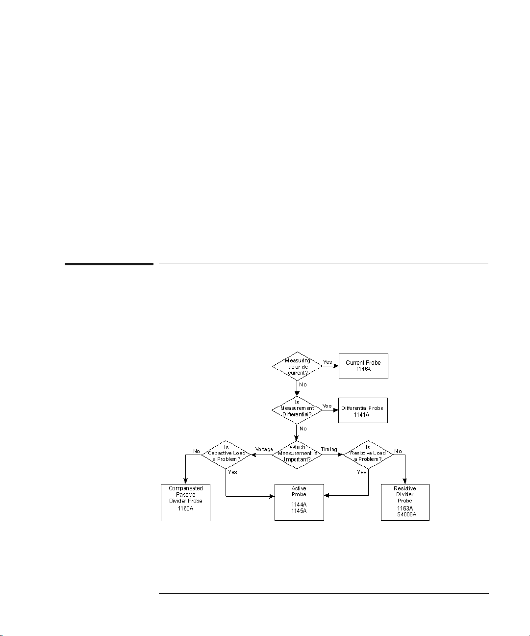
Selecting the Proper Probe
Use the flowchart below for selecting the proper type of probe. A
comparison of features, tradeoffs, and applications of the probes are
available after the flowchart.
Probing
1:1 Passive Probe
Features
No attenuation of waveform.
15
Page 16

Chapter 1: Agilent Technologies 16533/34A Digitizing Oscilloscope
Probing
Tradeoffs High capacitive loading and low bandwidth.
Applications Measuring small, low-bandwidth waveforms when no
attenuation can be tolerated such as power supply ripple.
Active Probe
Features
Best overall combination of low resistive and capacitive
loading. High bandwidth.
Tradeoffs Higher cost, limited dynamic range, requires power.
Applications ECL, CMOS, GaAs probing, analog circuit probing,
transmission line probing, source resistance
≥10 kohm, op amp
probing, most accurate for general measurements of circuits of
unknown impedance.
Compensated Passive Divider Probe
Features
Very low resistive loading, accurate amplitude measurements,
large dynamic range, and low cost.
Tradeoffs Capacitive loading <10 pF, lower bandwidth than active or
50-ohm resistive divider probes.
Applications General purpose probing, probing high-impedance nodes
≥10 Kohm), op amp probing, CMOS probing (if bandwidth is
(
adequate), TTL probing (if bandwidth is adequate)
Current Probe
Features
Measures both ac and dc currents on a scope, with minimal
circuit loading.
Tradeoffs Large size.
Applications Power measurements, automotive measurements,
industrial measurements, motors, dynamoes, and alternators.
Differential Probe
Features
High common mode rejection ratio, easy viewing of small
waveforms with large dc offsets, more accurate than subtracting one
channel from another.
16
Page 17

Chapter 1: Agilent Technologies 16533/34A Digitizing Oscilloscope
Probing
Tradeoffs Bigger than a passive probe, high cost, requires power, and
lower bandwidth than other probes.
Applications Measuring waveforms not referenced to the scope ground,
troubleshooting power supplies, and differential amplifier probing.
Resistive Divider Probe
Features
Highest bandwidth, lowest capacitive load, lower cost than
active probes, flat pulse response, good timing measurement accuracy.
Tradeoffs Relatively heavy resistive loading.
Applications ECL probing, GaAs probing, and transmission line probing.
See Also “Descriptions of Probe Types” on page 22
“Table of Compatible Probes” on page 14
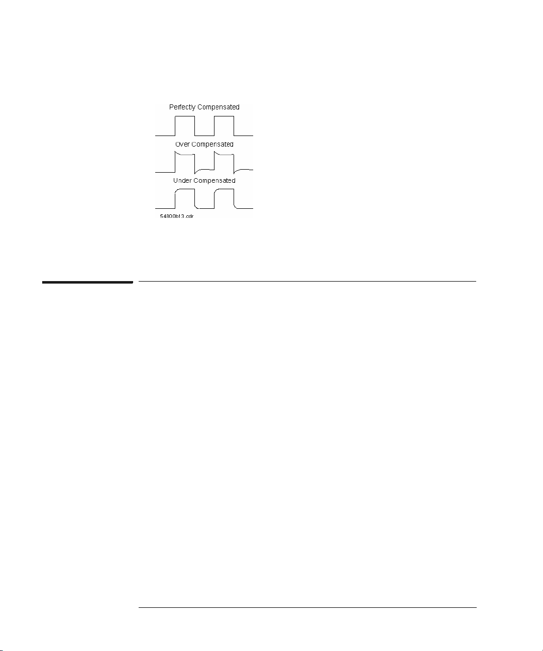
Compensating the Compensated Passive Divider Probe
Before you can have a flat frequency response when using a
Compensated Passive Divider Probe, the probe’s cable capacitance and
scope input capacitance must be compensated. One of the
compensating capacitors in the probe is adjustable so you can optimize
the step response for flatness.
1. Connect the probe to the BNC Output, labeled AC/DC CAL, on the back of
the oscilloscope.
2. Connect the probe ground lead to ground.
3. Select the oscilloscope icon and choose Calibration...
4. At the bottom of the calibration window, set BNC Output to Probe Comp
and close the window.
5. Select the oscilloscope icon and choose Setup/Display...
6. Select the Autoscale menu and choose Continue.
17
Page 18
Chapter 1: Agilent Technologies 16533/34A Digitizing Oscilloscope
Probing
7. You should see a waveform similar to one of the following.
8. If necessary, adjust the probe’s compensating capacitor. Set the scope to
keep running by selecting the Run Repetitive button.
Probe Loading
Probe Resistance and
Capacitance
Characteristics
There are two major factors influencing probe selection: the load the
probe imposes on your circuit and the required bandwidth of your
circuit with the probe. This is discussed in three sections, below.
Probe Resistance and Capacitance Characteristics (see page 18)
Probe Ground Lead Characteristics (see page 20)
Understanding System Bandwidth at the Probe Tip (see page 20)
The probe load has both resistive and capacitive components. In
addition, the inductance in the probe ground lead causes ringing.
The probe resistance to ground forms a voltage divider network with
the source resistance of your circuit. This reduces the waveform
amplitude and the dc offset. For example, if the probe’s resistance is 9
times the Thevenin equivalent resistance of your circuit, the waveform
amplitude is reduced by about 10 percent. Therefore, if your waveform
has a +5 V to 0.8 V range, the scope probe system shows a 4.5 V to 0.72
V range.
18
Page 19

Chapter 1: Agilent Technologies 16533/34A Digitizing Oscilloscope
NOTE: At high frequencies, the probe reactance dominates the resistance.
The probe capacitive loading (Cin) to ground forms an RC circuit with
the resistance of your circuit (R
the probe and scope (R
). The time constant of this RC circuit slows
in
) and the resistance looking into
source
the rise time of any transitions, increases the slew rate, and introduces
delay in the actual transition time. The approximate rise time of a
simple RC circuit is:
t
R
RC
Tot al
= 2.2R
= [RinR
Tot alCin
source
where
]/[Rin + R
source
]
Thus, for circuit resistance of 100 ohm, a scope probe system
resistance of 1 Mohm, and a probe capacitance of 8 pF, the real rise
time due to probe loading is:
= [1 Mohm (100 ohm)]/[1 Mohm + 100 ohm], approximately 100
R
Tot al
ohm.
= 2.2(100 ohm)(8 pF), approximately 1.8 ns.
t
RC
Probing
Therefore, the rise time of your circuit cannot be faster than
approximately 1.8 ns, even though it might be faster without the probe.
If the output of the circuit under test is current-limited (as is often the
case for CMOS), the slew rate is limited by the relationship dV/dT = I/C.
Perhaps you have connected a scope to a circuit for troubleshooting
only to have the circuit operate correctly after connecting the probe.
The capacitive loading of the probe can attenuate a glitch, reduce
ringing or overshoot of your waveform, or slow an edge just enough
that a setup or hold time violation no longer occurs.
19
Page 20

Chapter 1: Agilent Technologies 16533/34A Digitizing Oscilloscope
Probing
Probe Ground Lead
Characteristics
NOTE: If you print this page, subscripts and superscripts appear on the main line of
text. If a number seems to be in an odd place in the printed copy, it is probably
a superscript.
The inductance of the probe’s ground lead forms an LC circuit with the
probe’s capacitance and the output capacitance of the circuit under
test, including any parasitic capacitance of PC board traces, and so on.
The ringing frequency (F) of this circuit is:
F = (2 (3.14) (LC)
1/2)-1
If the rise time of the waveform is sufficient to stimulate this ringing,
the ringing can appear as part of your captured waveform. To calculate
the ringing frequency, you can assume that the probe’s ground lead has
an inductance of approximately 25 nH per inch. So, a probe with a
capacitance of 8 pF and a 4-inch ground lead has a ringing frequency of
approximately:
1/2)-1
F = (2 (3.14) [(25 nH) (4 inches) (8 pF)]
= 178 MHz
Understanding
System Bandwidth at
the Probe Tip
The 178 MHz does not include your circuit capacitance. Therefore, a
waveform with a rise time of less than 1.9 ns can stimulate ringing.
= 0.35/178 MHz = 1.9 ns
t
rise
To minimize the ringing effect, you should use a probe ground lead that
is as short as possible. Some probes add a ferrite bead to the ground
lead to reduce ringing. However, adding the ferrite bead also increases
the ground impedance which reduces the common mode rejection of
the probe.
System bandwidth is the bandwidth of the scope probe system. System
bandwidth affects measurements because the probe becomes part of
the circuit being measured. The rise time that is measured depends on
the actual rise time, the rise time of the scope probe system, and the
20
Page 21

Chapter 1: Agilent Technologies 16533/34A Digitizing Oscilloscope
Probing
rise time of the RC circuit formed by the source resistance and the
scope probe system resistance and capacitance.
t
meas
= [t
act
2
+ t
RC
2
+ t
sys
2
1/2
]
where
= the measured rise time.
t
meas
= the actual rise time of the waveform being measured.
t
act
= the rise time of the RC circuit formed by the source resistance
t
RC
and the scope probe system resistance and capacitance.
= the rise time of the scope probe system.
t
sys
NOTE: Often the bandwidth of the scope probe system is specified. The rise time is
calculated using the following equation.
= 0.35/SystemBW
t
sys
If the rise time of the scope probe system is not specified, it can be calculated
using the following formula.
probe
2
+ t
= [t
t
sys
scope
1/2
2
]
For example, if the scope probe system rise time is 600 ps, the probe
loading rise time (t
) is 600 ps, and the waveform has a 1-ns rise time,
RC
then the measured rise time is:
t
= [(1 ns)2 + (600 ps)2 + (600 ps)2]
meas
1/2
= 1.3 ns
The answer is in error by 30%.
However, if the scope probe system rise time is 190 ps, the probe
loading rise time is 190 ps, and the waveform has a 1-ns rise time, then
the measured rise time is:
= [(1 ns)2 + (190 ps)2 + (190 ps)2]
t
meas
1/2
= 1.03 ns
Now the error is only 3%.
You may find it useful to memorize three system bandwidth rules:
1. The combined rise time of the scope probe system and the probe loading
should be less than 1/3 of the rise time of the waveform you are measuring
to keep errors below 5%, and less than 1/7 of the rise time of the waveform
you are measuring to keep errors below 1%.
2. Rise time and bandwidth are related by the following approximations: rise
time = 0.35/bandwidth and bandwidth = 0.35/rise time.
21
Page 22

Chapter 1: Agilent Technologies 16533/34A Digitizing Oscilloscope
Probing
3. Rise times add approximately as the square root of the sum of the squares
(for systems with minimal peaking).
NOTE: Because every scope probe has a different loading effect on your circuit, you
should use the equation given for the type of scope probe you are using.
See Also “Descriptions of Probe Types” on page 22
Descriptions of Probe Types
For each of the probe types listed below, the description gives a
summary of features and tradeoffs and a short text description. Most of
the probe types also give a sample rise time calculation.
•“1:1 Passive Probes” on page 22
•“Active Probes” on page 24
•“Compensated Passive Divider Probes” on page 25
•“Current Probes” on page 27
•“Differential Probes” on page 27
•“Resistive Divider Probes” on page 28
1:1 Passive Probes
Features No attenuation of waveform.
Tradeoffs High capacitive loading and low bandwidth.
Applications Measuring small, low-bandwidth waveforms when no
attenuation can be tolerated such as power supply ripple.
The 1:1 passive probes provide a way to connect the input impedance
of the scope directly to your circuit with minimum attenuation due to
the resistive loading of the probe. However, 1:1 probes do have very
high capacitive loading which is much larger than that of the scope.
There are two types of 1:1 passive probes. One type is designed to work
22
Page 23

Chapter 1: Agilent Technologies 16533/34A Digitizing Oscilloscope
Probing
with the scope’s input set to high impedance (1 Mohm) and uses a
lossy cable to keep the probe from ringing. The other type is designed
to work with the scope’s input set to low impedance (50 ohm) and uses
a 50-ohm coaxial cable.
Example Rise Time
Calculation
Given the following circuit using the Agilent Technologies 1162A
probe,
the input resistance is:
= R
R
in
= 1 Mohm
scope
The total resisitance is:
= (RinR
R
Tot al
= 1 Mohm(50 ohm)/(1 Mohm + 50 ohm) = 50 ohm
R
Tot al
source
)/(Rin + R
source
)
From the Table of Compatible Probes, the probe capacitance is 50 pF.
Therefore, the capacitive load is:
= C
C
in
probe
+ C
= 50 pF + 7 pF = 57 pF
scope
The rise time due to circuit loading is:
= 2.2R
t
RC
Tot alCin
tRC = 2.2(50 ohm)(57 pF) = 6.2 ns
From the Table of Compatible Probes, the scope probe system has a
bandwidth of 25 MHz. Therefore, the rise time of the scope probe
system is: t
= 0.35/25 MHz = 14 ns
t
Sys
The measured rise time is: t
2
ns)
+ (6.2 ns)2 + (14 ns)2]
= 0.35/SystemBW
Sys
= [t
meas
1/2
= 140.8 ns
act
2
+ t
RC
2
+ t
sys
2
1/2
]
t
= [(140
meas
23
Page 24

Chapter 1: Agilent Technologies 16533/34A Digitizing Oscilloscope
Probing
Active Probes
Features Best overall combination of low resistive and capacitive
loading. High bandwidth.
Tradeoffs Higher cost, limited dynamic range, requires power.
Applications ECL, CMOS, GaAs probing, analog circuit probing,
transmission line probing, source resistance
probing, most accurate for general measurements of circuits of
unknown impedance.
An active probe has a buffer amplifier at the probe tip. This buffer
amplifier drives a 50-ohm cable terminated in 50 ohms at the scope
input. Active probes offer the best overall combination of resistive
loading, capacitive loading, and bandwidth.
≥10 kohm, op amp
Example Rise Time
Calculation
Given the following circuit using the Agilent Technologies 1152A
probe,
the input resistance is:
= 100 kohm. The total input resistance is:
R
in
= (RinR
R
Tot al
= 100 ohm(50 ohm)/(100 ohm + 50 ohm) = 50 ohm
R
Tot al
source
)/(Rin + R
source
)
The rise time due to circuit loading is:
= 2.2R
t
RC
Tot alCtip
tRC = 2.2(50 ohm)(0.6 pF) = 66 ps
Because the rise time of the scope probe system is not given in the
Table of Compatible Probes, we will have to calculate it using the
24
Page 25

Chapter 1: Agilent Technologies 16533/34A Digitizing Oscilloscope
Probing
bandwidth of the probe (2.5 GHz) and the bandwidth of the scope (500
MHz). Therefore, the rise time of the scope probe system is:
= 0.35/ProbeBW = 0.35/2.5 GHz = 140 ps
t
probe
= 0.35/ScopeBW = 0.35/500 MHz = 700 ps
t
scope
t
= [t
sys
t
= [(140 ps)2 + (700 ps)2]
sys
probe
2
+ t
scope
2
1/2
]
1/2
= 714 ps
The measured rise time is:
t
meas
= [t
act
2
+ t
RC
2
+ t
sys
2
1/2
]
t
= [(2 ns)2 + (66 ps)2 + (714 ps)2]
meas
1/2
= 2.12 ns
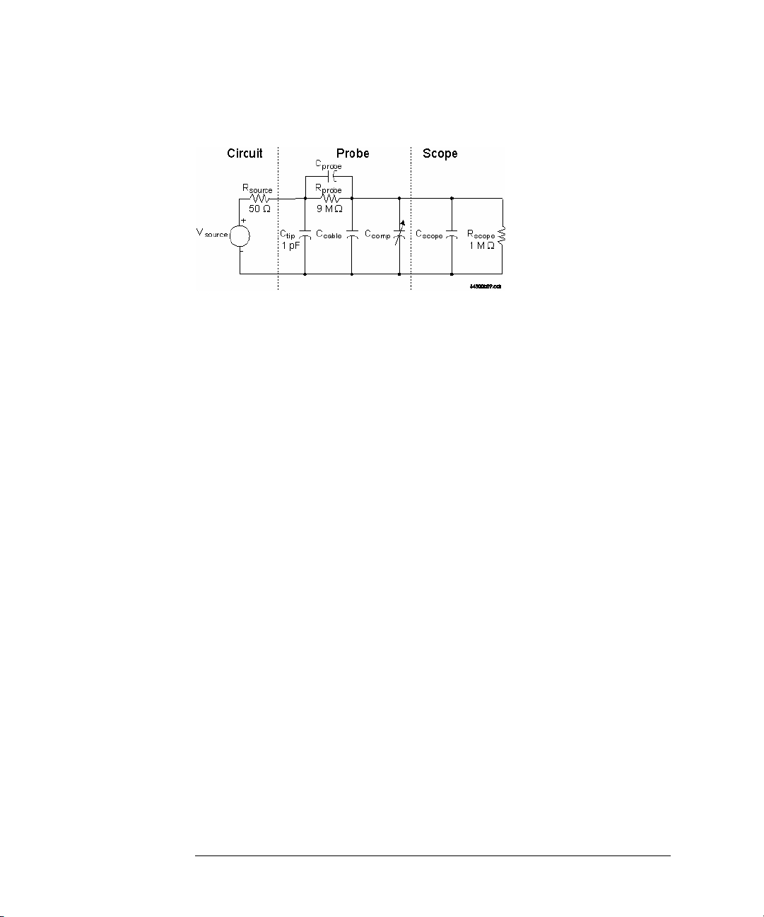
Compensated Passive Divider Probes
Features Very low resistive loading, accurate amplitude measurements,
large dynamic range, and low cost.
Tradeoffs Capacitive loading <10 pF, lower bandwidth than active or
50-ohm resistive divider probes.
Applications General purpose probing, probing high-impedance nodes
≥10 Kohm), op amp probing, CMOS probing (if bandwidth is
(
adequate), TTL probing (if bandwidth is adequate).
The compensated passive divider probe is the most common type of
scope probe. The 9-Mohm resistor in the tip forms a 10:1 voltage
divider with the 1-Mohm input resistance of the scope.
To have a flat frequency response, the probe tip capacitance is
compensated by the probe’s cable capacitance, a compensating
capacitor, and the scope input capacitance. The compensating
capacitor is adjustable so you can optimize the step response for
flatness.
Not all 9-Mohm divider probes work with all 1-Mohm scope inputs. The
probe data sheet shows the range of scope input capacitance it can
accommodate. You must make sure that the input capacitance of the
scope is within that range.
25
Page 26
Chapter 1: Agilent Technologies 16533/34A Digitizing Oscilloscope
Probing
Example Rise Time
Calculation
Given the following circuit using an Agilent Technologies 1160A probe,
the input resistance is:
= R
R
in
= 9 Mohm + 1 Mohm = 10 Mohm
R
in
probe
+ R
scope
The capacitive load is:
= C
C
in
[C
probe+Ccable+Ccomp+Cscope
tip
+ {[C
probe(Ccable+Ccomp+Cscope
]}
)]/
This number is calculated for the scope and scope probe combination,
and is shown in the Table of Compatible Probes.
The total resistance is: R
= 10 Mohm(50ohm)/(10 Mohm + 50ohm) = 50 ohm
R
Tot al
Total
= (RinR
source
)/(Rin + R
source
)
The rise time due to circuit loading is: t
= 2.2R
RC
Tot alCin
tRC = 2.2(50 ohm)(7.5 pF) = 825 ps
From the Table of Compatible Probes, the bandwidth of the scope
probe system is 500 MHz. Therefore, the rise time of the scope probe
system is:
= 0.35/SystemBW
t
sys
= 0.35/500 MHz = 700 ps
t
sys
The measured rise time is:
= [(t
t
meas
t
= [(2 ns)2 + (825 ps)2 + (700 ps)2]
meas
)2 + (tRC)2 + (t
act
sys
)2]
1/2
1/2
= 2.27 ns
Remember that probe input impedance for compensated passive
divider probes is complex. A simple RC network serves only as a firstorder approximation.
26
Page 27

Chapter 1: Agilent Technologies 16533/34A Digitizing Oscilloscope
Probing
Current Probes
Features Measures both ac and dc currents on a scope, with minimal
circuit loading.
Tradeoffs Large size.
Applications Power measurements, automotive measurements,
industrial measurements, motors, dynamoes, and alternators.
Scopes are designed to measure voltage, but by using a current probe
you can measure current. A current probe measures current in a wire
by enclosing the wire. Therefore, no electrical connection is needed.
Current probes generally use one of two technologies. The simplest
uses the principle of a transformer, with one winding of the
transformer being the measured wire. Because transformers only work
with alternating voltages and currents, current probes of this type
cannot measure direct current.
The other type of current probe uses the Hall effect principle. The Hall
effect produces an electric field in response to an applied magnetic
field. While this technique requires a power supply, it measures both
alternating and direct current.
Differential Probes
Features High common mode rejection ratio, easy viewing of small
waveforms with large dc offsets, more accurate than subtracting one
channel from another.
Tradeoffs Bigger than a passive probe, high cost, requires power, and
lower bandwidth than other probes.
Applications Measuring waveforms not referenced to the scope ground,
troubleshooting power supplies, and differential amplifier probing.
A differential probe is a high-impedance differential amplifier with two
probe tips; a non-inverting input and an inverting input. These two
inputs feed a differential amplifier which in turn drives the 50-ohm
input of the scope. The main advantage of differential probes is their
ability to reject waveforms that are common to both inputs. This type
of probe is often used in floating ground applications.
27
Page 28

Chapter 1: Agilent Technologies 16533/34A Digitizing Oscilloscope
Probing
You could duplicate a differential probe by using two passive probes
and subtracting the two scope channels. However, the electrical paths
of the differential probe are carefully matched to give a high common
mode rejection ratio (CMRR). The higher the CMRR, the smaller the
waveforms you can view in the presence of unwanted noise.
Resistive Divider Probes
Features Highest bandwidth, lowest capacitive load, lower cost than
active probes, flat pulse response, good timing measurement accuracy.
Tradeoffs Relatively heavy resistive loading.
Applications ECL probing, GaAs probing, and transmission line
probing.
Resistive divider probes are designed for scopes with a 50-ohm input
impedance. The probe tips of the Agilent Technologies 1163A or
54006A have either a 450-ohm or 950-ohm series resistor. The probe
cable is a 50-ohm transmission line. Because the cable is terminated in
50 ohms at the scope input, it looks like a purely resistive 50-ohm load
when viewed from the probe tip. Therefore, the resistive divider probe
is flat over a wide range of frequencies, limited primarily by the
parasitic capacitance and inductance of the 450-ohm or 950-ohm
resistor and the fixture that holds it. The resistive load of the probe to
your circuit is either 500 ohm or 1 kohm, depending on the probe.
Example Rise Time
Calculation
This type of probe has the smallest capacitive load of any probe. The
small capacitance and wide bandwidth make this probe type a good
choice for wide bandwidth measurements or time-critical
measurements.
Given the following circuit using the Agilent Technologies 1163A
probe,
28
Page 29
Chapter 1: Agilent Technologies 16533/34A Digitizing Oscilloscope
the input resistance is:
= R
R
in
R
in
+ R
tip
= 450 ohm + 50 ohm = 500 ohm
scope
The total resistance is:
= (RinR
R
Tot al
= 500 ohm(50ohm)/(500 ohm + 50ohm) = 45 ohm
R
Tot al
source
)/(Rin + R
source
)
Probing
The rise time due to circuit loading is:
= 2.2R
t
RC
Tot alCtip
tRC = 2.2(45 ohm)(1.5 pF) = 165 ps
From the Table of Compatible Probes, the bandwidth of the scope
probe system is 1.5 GHz. Therefore, the rise time of the scope probe
system is:
= 0.35/SystemBW
t
sys
= 0.35/1.5 GHz = 230 ps
t
sys
The measured rise time is:
= [(t
t
meas
t
= [(2 ns)2 + (165 ps)2 + (230 ps)2]
meas
)2 + (tRC)2 + (t
act
sys
)2]
1/2
1/2
= 2.02 ns
Surface Mount Probing
The Agilent Technologies 10467A 0.5 mm MicroGrabber Accessory Kit
is designed for using the Agilent Technologies 116x family of probes
when you are probing fine-pitch (0.5 mm to 0.8 mm) SMT (Surface
29
Page 30

Chapter 1: Agilent Technologies 16533/34A Digitizing Oscilloscope
Probing
Mount Technology) devices. The kit contains enough parts for two
probes.
The Agilent Technologies 116x probe tip plugs into the single-lead end
of the dual-lead adapter. The MicroGrabber connects to the red lead.
You can also use a MicroGrabber on the black lead, which you should
connect to your circuit’s ground. You can also connect the dual-lead
end to circuit pins that are 0.635 mm (0.025 inch) in diameter.
The kit is intended for use with voltages no greater than
ac peak).
±40 V (dc and
30
Page 31

Chapter 1: Agilent Technologies 16533/34A Digitizing Oscilloscope
Acquiring a Waveform
Acquiring a Waveform
The two ways to acquire a waveform with the oscilloscope are
Autoscale and Run. When you use Run, you can modify settings to
fine-tune your measurement.
You can also save acquired waveforms using waveform memories. (see
page 78)
Autoscale
Autoscale automatically adjusts volts per division and offset so that the
waveform fits into the display. It also attempts to set the seconds per
division so that three periods of the waveform are displayed.
Specifying a Measurement
To set up a measurement, first specify the channel setup then the
trigger. Based on your waveform you may need to change the offset
and scale to get accurate measurements.
A faster way to set up your measurement is to first autoscale, then
adjust only the settings you are interested in.
Running
The default acquisition mode is single-shot. To take another acquisition
immediately after the first one, select the Run Repetitive button.
The scope does not support any modes other than real-time mode. You
can turn on averaging or accumulate under the Display tab. However,
because of the way the oscilloscope samples, this is not the same as the
equivalent time mode of a stand-alone oscilloscope.
NOTE: Selecting the Run button in an instrument window only runs that instrument.
To run all active instruments, select Run All in the System or Workspace
window, or Group Run in the window of any instrument included in a group
run. If the scope is triggered by another instrument, do not change settings
while the scope is waiting for its trigger or it may not trigger.
See Also “Run/Group Run Function” on page 90
31
Page 32

Chapter 1: Agilent Technologies 16533/34A Digitizing Oscilloscope
Acquiring a Waveform
“Autoscale” on page 32
“Specifying a Measurement” on page 33
“Using Waveform Memories” on page 78
“Differences from a Standard Digitizing Oscilloscope” on page 77
“Combining the Oscilloscope with a Logic Analyzer” on page 35
Autoscale
Autoscale automatically optimizes the waveform display for each
channel that is turned on. It sets volts per division and offset so that
the waveform fits into the middle of the display, and adjusts the
timebase (horizontal axis) to show three periods. When signals have
different periods, the signal on the lowest-numbered channel is used to
set the horizontal scale. If none of the signals show activity, the
timebase is set to 200 ns per division.
Autoscale also changes the trigger settings. The trigger channel is
channel 1 unless the signal on channel 1 has no detectable voltage
change. Triggering is limited to channels 1 and 2; no higher-numbered
channels can be set, but they will be autoscaled. The trigger mode is
set to the first rising edge and autotriggered. The trigger level is set to
the 60% threshold of the signal. If both channel 1 and channel 2 have
flat signals, the trigger source is set to channel 2 and the trigger level is
set to channel 2’s offset.
The settings changed by autoscale are:
Setting Default Algorithm
V/div 200 mV/div Waveform fits within the middle
(Scale) 6 divisions of the display
Channel Offset 0 Waveform is centered vertically
Sec/div 200 ns/div Fit three periods on screen
(Scale)
Time offset 0 Always centers waveform around trigger
(Delay)
Trigger mode rising edge Always sets trigger to rising edge
Trigger sweep autotrigger Always sets trigger to autotrigger
32
Page 33

Chapter 1: Agilent Technologies 16533/34A Digitizing Oscilloscope
Acquiring a Waveform
Trigger level not applicable Always sets level to near 60% threshold
if a non-constant signal is detected
Trigger occurrence 1 Always sets occurrence to 1
Trigger source channel 1 Checks channel 1 for an active signal;
if signal is flat, sets to channel 2
Specifying a Measurement
1. Connect probes. (see page 14)
2. Set up the channel. (see page 33)
3. Set the display mode. (see page 59)
4. Specify trigger. (see page 38)
5. Select the Run Repetitive button to start the acquisition.
6. Save particular waveforms to waveform memory. (see page 78)
The data is automatically displayed in the oscilloscope window. You can
also connect it to a display tool in order to correlate the oscilloscope
with a logic analyzer.
See Also “Combining the Oscilloscope with a Logic Analyzer” on page 35
“Probing” on page 14
“Channel Setup Window” on page 33
“Display Setup Window” on page 59
“Triggering” on page 38
“Using Waveform Memories” on page 78
Channel Setup Window
To access the Channel Setup window, select the Setup... button under
the Channels tab. Use this window to specify your probe type and
probe impedance. After the initial setup, you may want to use this
window to adjust channel skew.
On/Off Use this button to turn the channel on or off. You can also do
33
Page 34

Chapter 1: Agilent Technologies 16533/34A Digitizing Oscilloscope
Acquiring a Waveform
this from the main oscilloscope window.
Name Channel names can be a maximum of 10 characters long.
Customized names appear anywhere the channel is labeled.
Probe The probe attenuation factor. The arrow keys scroll through the
standard probe attenuation values, or you can enter non-standard
values by typing in the field. Probe attenuation affects the display and
marker measurements.
Input Z / Coupling Probe input impedance. Incorrect impedance will
cause bad measurements. See the “Table of Compatible Probes” on
page 14 for suggested values.
Skew Adjust for channel-to-channel skew caused by differing
electrical path lengths of the probes. To deskew the channels for multiboard oscilloscopes, run Channel Skew in the calibration utility.
Preset Select from TTL, ECL, and User. TTL sets the scale to 1 V/div
and the offset to 2.50 V. ECL sets the scale to 250 mV/div and the offset
to -1.3 V. User defaults to TTL values, but if you change the Scale or
Offset settings, the Preset field changes to User.
Scale Scale affects the vertical axis of the waveform display. You can
change it through either the arrow buttons or by typing in the field. It is
the same scale field as in the main oscilloscope window.
Offset Offset moves the waveform vertically in the display window.
Parts of the waveform that go offscreen are clipped, which may affect
any automatic measurements you run. The offset field also appears in
the main oscilloscope window.
You can also display the Channel Setup window by selecting a channel
in the grid and choosing Channels... from the menu.
See Also “Calibrating the Oscilloscope” on page 10
“Probing” on page 14
“Vertical and Horizontal Scaling” on page 52
34
Page 35

Chapter 1: Agilent Technologies 16533/34A Digitizing Oscilloscope
Combining the Oscilloscope with a Logic Analyzer
Combining the Oscilloscope with a Logic
Analyzer
If you want to make a measurement with a logic analyzer and an
oscilloscope, there are three cases:
•“Oscilloscope Triggers Logic Analyzer” on page 35
•“Logic Analyzer Triggers Oscilloscope” on page 36
•“Logic Analyzer and Oscilloscope Correlate Data” on page 36
See Also The Intermodule Window (see the Agilent Technologies 16700A/B-Series
Logic Analysis System help volume) for a generic approach.
Oscilloscope Triggers Logic Analyzer
1. Select the toolbar's Workspace button.
2. In the Workspace window, drag both instruments on to the workspace.
3. Connect both to the same display tool.
4. In the Correlation Error dialog that appears, select Group Run for the
scope and Oscilloscope for the logic analyzer.
5. Select the Group Run or Run All button to start the acquisition.
6. To view the waveforms together, open the display tool.
• For a Waveform display, select one of the labels and choose Insert
before... or Insert after.... In the Label Dialog, select the label you want
to insert, then select the Apply button.
• For the other tools, the oscilloscope labels are already available.
35
Page 36

Chapter 1: Agilent Technologies 16533/34A Digitizing Oscilloscope
Combining the Oscilloscope with a Logic Analyzer
Logic Analyzer Triggers Oscilloscope
NOTE: When the logic analyzer triggers the oscilloscope, if you are changing
oscilloscope settings when the trigger occurs it may be missed. The message
bar and Run Status window show "Waiting for IMB Arm" when this occurs.
When this happens, select the Stop button and restart the acquisition.
1. Select the toolbar’s Workspace button.
2. In the Workspace window, drag both instruments on to the workspace.
3. Connect both to the same display tool.
4. In the Correlation Error dialog that appears, select Group Run for the
logic analyzer and the logic analyzer description for the oscilloscope.
5. A Trigger Advisory dialog box may appear. Select Trigger Immediate.
6. Select the Group Run or Run All button to start the acquisition.
7. To view the waveforms together, open the display tool.
• For a Waveform display, select one of the labels and choose Insert
before... or Insert after.... In the Label Dialog, select the label you want
to insert, then select the Apply button.
• For the other tools, the oscilloscope labels are already available.
Logic Analyzer and Oscilloscope Correlate Data
1. Select the toolbar's Workspace button.
2. In the Workspace window, drag both instruments on to the workspace.
3. Connect both into same display tool.
4. In the Correlation Error dialog that appears, select Group Run for both
instruments.
5. Select the Group Run or Run All button to start the acquisition.
36
Page 37

Chapter 1: Agilent Technologies 16533/34A Digitizing Oscilloscope
Combining the Oscilloscope with a Logic Analyzer
6. To view the waveforms together, open the display tool.
• For a Waveform display, select one of the labels and choose Insert
before... or Insert after.... In the Label Dialog, select the label you want
to insert, then select the Apply button.
• For the other tools, the oscilloscope labels are already available.
37
Page 38

Chapter 1: Agilent Technologies 16533/34A Digitizing Oscilloscope
Tr ig ge ri ng
Triggering
The default trigger type is auto, which means the oscilloscope will
trigger after 100 milliseconds. The trigger appears in the center of the
acquisition. You can change where the trigger is in the data set by
using the Delay field.
To specify more complicated triggers, select the Trig g e r... button at
the bottom of the main oscilloscope window. This brings up the Trigger
Setup Window.
You can also display the Trigger Setup window by selecting the trigger
marker and choosing Tri g g e r... from the menu.
The area to the right of the Trigger button indicates the current trigger.
It does not show details such as occurence count.
•“Trigger Concepts” on page 38
•“Edge Triggering” on page 40
•“Pattern Triggering” on page 41
•“Delayed Triggering” on page 42
•“Getting a Stable Trigger” on page 43
•“The Trigger Setup Window” on page 44
Trigger Concepts
Trigger B a s ics
The scope trigger circuitry helps you locate the waveform you want to
view. There are several types of triggering, but the one that is used
most often is edge triggering. Edge triggering identifies a trigger
condition by looking for the slope (rising or falling) and voltage level
38
Page 39
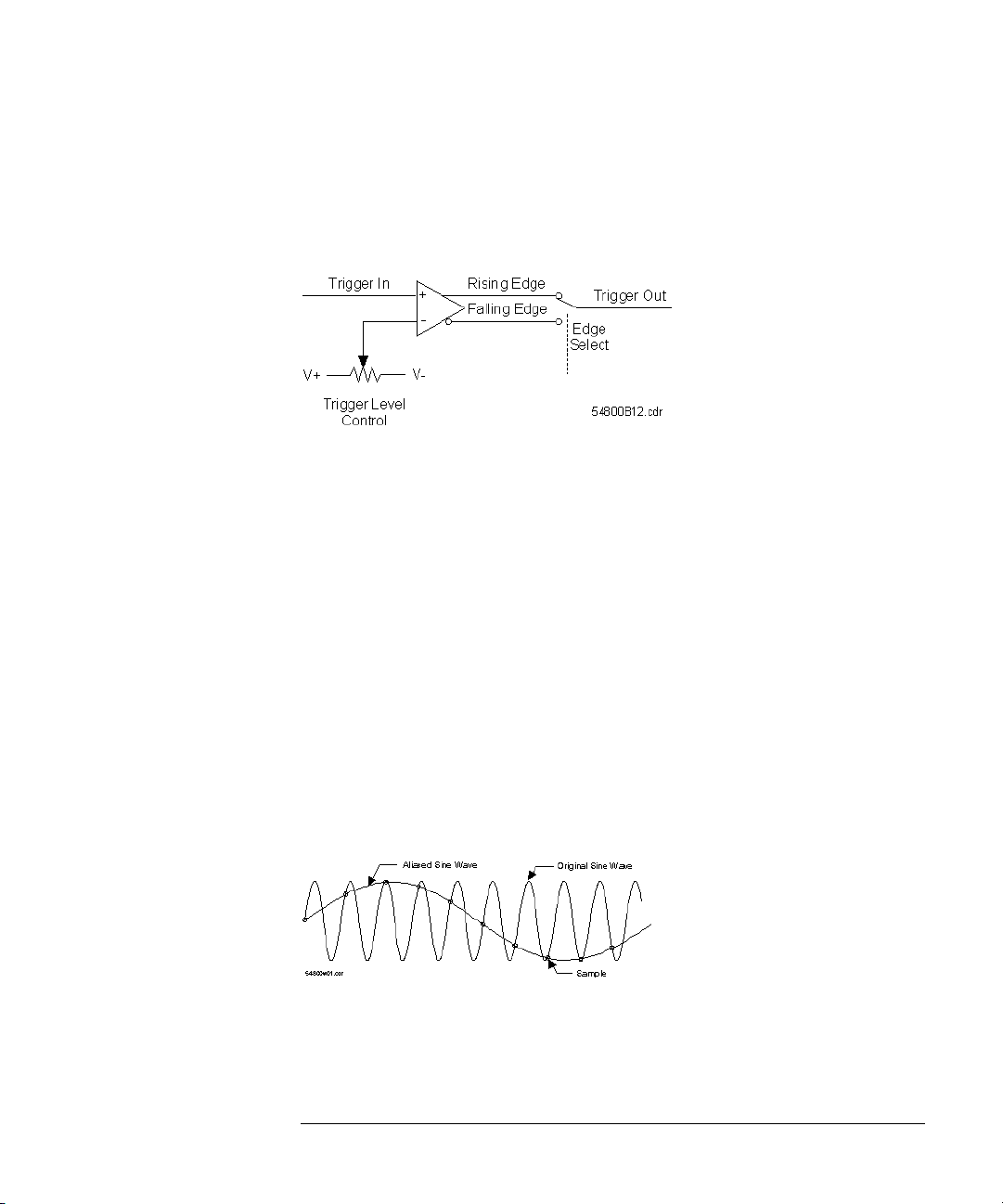
Chapter 1: Agilent Technologies 16533/34A Digitizing Oscilloscope
Trig ge ri ng
(trigger level) on the source you select. The trigger source is restricted
to channel 1, channel 2, and the external trigger. If you have more
channels on your oscilloscope, they cannot be used as trigger sources.
This figure shows the trigger circuit diagram.
Your waveform enters the positive input to the trigger comparator
where it is compared to the trigger level voltage on the other input. The
trigger comparator has a rising edge and a falling edge output. When a
rising edge of your waveform crosses the trigger level, the rising edge
comparator output goes high and the falling edge output goes low.
When a falling edge of your waveform crosses the trigger level, the
rising edge output goes low and the falling edge output goes high. The
scope uses the output you have selected as the trigger output.
Aliasing and Triggering
While aliasing does not cause unstable triggering, it does make it
difficult to tell when the scope is triggered. An aliased waveform can
appear as a lower frequency waveform that drifts across the display. To
ensure that your waveform is not aliased, you should decrease the
horizontal scale to its minimum value (maximum sampling rate), then
increase it to view your waveform.
39
Page 40

Chapter 1: Agilent Technologies 16533/34A Digitizing Oscilloscope
Tr ig ge ri ng
Edge Triggering
Edge trigger is the default trigger setting. Edge mode sets the
oscilloscope to trigger on an edge. You can set the source, trigger level,
and slope in the oscilloscope main window. Selcting the Trigger...
button brings up the Trigger Setup window, which lets you set the
number of edges.
You can also display the Trigger Setup window by selecting the trigger
marker and choosing Tri g g e r... from the menu.
The oscilloscope identifies an edge trigger by looking for the specified
slope (rising edge or falling edge) of your waveform. Once the slope is
found, the oscilloscope will trigger when your waveform crosses the
trigger level.
If you set the source to External, the trigger level is fixed at -1.30 V.
NOTE: The oscilloscope always fills a certain amount of acquisition memory before
looking for a trigger. When counting edge occurrences, you may see more
edges before the trigger than the number you specified. This happens because
some edges were already in memory but are not included in the occurrence
count.
When you set the trigger level on your waveform, it is usually best to
set it to a voltage near the middle of your waveform. The middle range
is best because there may be ringing or noise at the high and low ends
which can cause false triggers.
When you adjust the arm level control, a horizontal dashed line with a
T on the right-hand side appears, showing you where the arm level is
with respect to your waveform. After a period of time the dashed line
will disappear. You can get the line back by adjusting the arm level
control again.
40
Page 41

Chapter 1: Agilent Technologies 16533/34A Digitizing Oscilloscope
Trig ge ri ng
Pattern Triggering
Pattern triggering is similar to the way that a logic analyzer captures
data. This mode is useful when you are looking for a particular set of
ones and zeros on a computer bus or control lines. You can use channel
1 and 2 and the external trigger to form the trigger pattern. Because
you can set the voltage level that determines a logic 1 or a logic 0, any
logic family that you are probing can be captured. Channels 3 through
8, available in multi-board oscilloscopes, cannot be used in the pattern.
You can display the Trigger Setup window by selecting the trigger
marker and choosing Tri g g e r... from the menu.
When Pattern
There are five ways you can use to further qualify the pattern that you
want to view. They are:
Entered When the scope finds the pattern, it triggers on the edge of
the pulse that makes the pattern valid.
Exited The scope arms the trigger circuitry when it has found the
pattern and triggers on the edge of the pulse that ends the
pattern.
Present > The scope triggers when the pattern is found and is present
for greater than the time value that you specify.
Present < The scope triggers when the pattern is found and is present
for less than the time value that you specify.
Range > The scope triggers when the pattern is present within the
time range that you specify.
NOTE: For Present >, Present <, and Range >, the oscilloscope does not trigger until
the pattern is exited.
1. Set up a pattern by selecting the X button after each channel name.
41
Page 42

Chapter 1: Agilent Technologies 16533/34A Digitizing Oscilloscope
Tr ig ge ri ng
X means the channel is not part of the pattern.
Low and High let you set the threshold voltages for channel 1 and channel
2.
2. Select the When Pattern that you want.
3. If you have selected Present >, Present <, or Range >, set the time values.
The minimum is 20 ns, and the maximum is 160 milliseconds.
4. Close the Trigger Setup dialog box.
The area to the right of Trigger... shows the pattern you set up.
Delayed Triggering
You can delay the trigger by setting the Delay field. The Delay field
changes the acquisiton delay. Acquisition delay is the amount of time
between the trigger event and the center of the acquisition. It is the
only way to change the pre-trigger and post-trigger amounts in the
Agilent Technologies 16533A or 16534A Digitizing Oscilloscope.
To Store Mostly PostTrigger Data
The value shown in the Delay field is the sum of the acquisition delay
and the display delay. The display delay is controlled by the scrollbar,
and indicates which portion of the acquisition is currently being
displayed.
1. Calculate 16,350 (about half the acquisition memory) divided by the
sample rate. You should get a value in seconds.
2. Enter that value in the delay field.
Use n for nanoseconds, u for microseconds, and m for milliseconds.
3. If the value is correct, the scrollbar will move to one end of its range and
the current signal will not cross the entire display.
4. Select the Run button. The scrollbar returns to the middle.
If you adjust the scrollbar before seleing the Run button, the oscilloscope
treats the value as a display delay only.
To store mostly pre-trigger data, calculate the same value and enter it
as a negative number.
42
Page 43

Chapter 1: Agilent Technologies 16533/34A Digitizing Oscilloscope
Trig ge ri ng
To Re-center the
Trigger in the
Acquisition
See Also “Vertical and Horizontal Scaling” on page 52
1. Drag the scrollbar to the center of the scroll area. There is a slight delay in
movement when the bar is at the center.
2. Set Delay at the bottom of the window to 0 seconds, and press enter.
The scrollbar may jump away from the center. Do not reset it.
3. Select the Run button to get a new acquisition.
Getting a Stable Trigger
For most waveforms, the easiest way for you to get a stable trigger is to
use Autoscale. Autoscale analyzes your waveform and sets the trigger
mode to edge and the vertical scale, horizontal scale, and trigger level
to best display your waveform.
Manual Triggering
While Autoscale is the easiest way to obtain a stable trigger, there are
times when you may need to set the trigger manually to capture more
complex waveforms. To stabilize these waveforms:
• Set the Trigger Level to the proper point on the waveform.
The proper point is usually somewhere around 50% to avoid possible
ringing and noise at the top and base voltages.
• Increase the sampling rate to avoid aliasing.
The sampling rate is controlled by the horizontal scale at the bottom of the
screen. The maximum sampling rates are 1 gigasample per second for the
16533A and 2 gigasamples per second for the 16534A.
• Set the Trigger Sweep to Triggered for low-frequency waveforms.
The Trigger Sweep field is in the Trigger Setup dialog.
• Remove noise from your waveform.
43
Page 44

Chapter 1: Agilent Technologies 16533/34A Digitizing Oscilloscope
Tr ig ge ri ng
You can display the Trigger Setup window by selecing the trigger
marker and choosing Tri g g e r... from the menu.
See Also “The Trigger Setup Window” on page 44
“Autoscale” on page 32
“Changing the Sample Rate” on page 54
The Trigger Setup Window
The Trigger Setup window is for setting up complex triggers. You
access it by selecting the Trig g e r... button at the bottom of the main
oscilloscope window.
The two selections that are always availabe in the window are Mode
and Sweep. Mode specifies the type of condition you want to trigger
on. Sweep indicates whether the oscilloscope should wait for the
condition (Tri ggered) or trigger immediately if the condition doesn’t
show up in 100 milliseconds (Auto).
Edge
Pattern
Edge mode sets the oscilloscope to trigger on an edge. You can specify
the source, trigger level, slope, and occurrence.
The oscilloscope identifies an edge trigger by looking for the specified
slope (rising edge or falling edge) of your waveform. Once the slope is
found, the oscilloscope will trigger when your waveform crosses the
trigger level.
If you set the source to External, the trigger level is fixed at -1.30 V.
Use pattern mode for triggering on glitches or unusually long pulses, or
for a trigger involving 2 channels.
To Trigger on a Glitch
1. Select the Tr i g ger.. . button.
2. Set the mode to Pattern and the sweep to Triggered.
44
Page 45

Chapter 1: Agilent Technologies 16533/34A Digitizing Oscilloscope
Trig ge ri ng
3. Specify the glitch source by setting it to high or low. An X means the
channel is not part of the pattern.
4. Select the option button under When Pattern and choose Present <.
5. Set the duration field to less than your clock’s pulse width.
Immediate
Use immediate mode when the oscilloscope is triggered by another
instrument in the measurement, or to acquire data as soon as you
select the Run button. No other levels or settings may be specified for
this mode.
You can also display the Trigger Setup window by selecting the trigger
marker and choosing Tri g g e r... from the menu.
See Also “Edge Triggering” on page 40
“Pattern Triggering” on page 41
“Trigger Concepts” on page 38
45
Page 46

Chapter 1: Agilent Technologies 16533/34A Digitizing Oscilloscope
Changing Waveform Display and Grid
Changing Waveform Display and Grid
•“Zooming In” on page 46
•“Changing the Persistence of the Waveform” on page 46
•“Viewing Noisy Waveforms with Averaging” on page 48
•“Changing Display Colors” on page 50
•“Changing the Grid” on page 50
Zooming In
To zoom in on a particular area of your waveform, drag a selection
rectangle over the area and release.
To undo zoom, select in the display area and choose Undo Zoom. You
can also choose Undo Zoom from the Setup menu.
Zoom may change your vertical scale (V/div), offset value, horizontal
scale (timebase or s/div), and scrollbar position to match the current
section of the waveform as though you had acquired it in that state.
When the new settings exceed limits, the display change does not
occur. This is most likely to happen with extreme negative delays and
detailed vertical scaling (V/div). You may be able to zoom in if you
enclose a larger area in the zoom.
If you Run then Undo Zoom, the original settings will be restored, but
your waveform may look wrong. The gaps are due to clipping; the
Agilent Technologies 16533A or 16534A oscilloscopes treat clipped
data by leaving it at the top and bottom edges of the display.
Changing the Persistence of the Waveform
Normally, a waveform is displayed only for one acquisition. When the
next run occurs, the previous waveform is erased and the newly
46
Page 47

Chapter 1: Agilent Technologies 16533/34A Digitizing Oscilloscope
Changing Waveform Display and Grid
acquired waveform is drawn on the display.
By using accumulate, you can see a visual history of a waveform’s
acquisitions over time. For example, you can see the accumulated
peak-to-peak noise of a waveform over time which may appear
significantly different than in only one acquisition. You can see timing
jitter, the variance of the waveform from the trigger event, by
accumulating acquisitions on the display. By using accumulate, viewing
a waveform’s extremes over time is much easier.
Waveform mode sets the amount of time a waveform sample appears
on the display. Automated measurements cannot be performed on
accumulated waveforms but will be performed on the most recent
waveform in acquisition memory. Waveform accumulation does not
occur beyond the display area boundary.
The Agilent Technologies 16533A or 16534A Digitizing Oscilloscope
have three waveform modes: Normal, Accumulate, and Average.
Normal
In the normal waveform mode, a waveform data point is displayed for
at least 10 ms or one trigger cycle then erased. If no further triggers
occur, the last acquisition is left on the display. This is the default
setting. Use this mode for the fastest display update rate.
Accumulate
Accumulate is most like infinite persistence. In the accumulate
waveform mode, a waveform sample point is displayed until settings
are changed. All sample points are shown at full intensity. Use
accumulate to measure jitter or eye diagrams, see a waveform’s
envelope, look for timing violations, and find infrequent events.
Average
When Averaging is enabled, the # Avgs control tells the oscilloscope
the number of waveforms you want to use in calculating the average
value for each sample point. The Agilent Technologies 16533A or
16534A oscilloscopes can average from 2 to 512 waveform acquisitions
but the larger the number of acquisitions, the more time it will take to
accumulate all the waveforms you have requested.
47
Page 48

Chapter 1: Agilent Technologies 16533/34A Digitizing Oscilloscope
Changing Waveform Display and Grid
NOTE: If you are using Accumulate or Average and you change the vertical or
horizontal scaling, position, offset, trigger source or level, zoom, or drag the
waveform then the display is redrawn and any accumulated waveforms are
cleared. Only the last acquisition is displayed.
Set up markers and any measurements before using accumulate or averaging.
Adding markers or clearing measurements later can erase acquired
waveforms.
See Also “Viewing Noisy Waveforms with Averaging” on page 48
“Display Setup Window” on page 59
Viewing Noisy Waveforms with Averaging
The Waveform Average mode under Display tells the oscilloscope to
acquire waveforms from several acquisitions and average them all
together, point by point. The greater the number of averages, the less
impact each new waveform has on the composite averaged waveform.
The perceived display update rate is slowed down as the number of
averages is increased because the averaged waveform doesn’t change
as much.
Sometimes, a waveform consists of a signal along with some random or
asynchronous noise. By using Waveform Average, these noise sources
can average to zero over time while the underlying waveform is
preserved. This will improve the accuracy of waveform measurements
because measurements are made on a more stable waveform and
measurement variances are reduced. The effective resolution of the
displayed waveform also improves as more acquisitions are averaged
together, providing the input waveform is repetitive and has a stable
trigger point.
Incidentally, if Waveform Average is enabled but the scope is not
properly triggering (perhaps the scope is set to Auto trigger and the
wrong trigger channel is selected), you may not see the waveform you
expect on the display. In this case, the input waveform is asynchronous
to the scope and will average to zero over time even though a non-zero
48
Page 49

Chapter 1: Agilent Technologies 16533/34A Digitizing Oscilloscope
Changing Waveform Display and Grid
input waveform is being measured.
When Waveform Average is enabled, the # Avgs control sets the
number of waveforms you want to use in calculating the average value
for each sample point. The Agilent Technologies 16533A or 16534A can
average from 2 to 512 waveform acquisitions but the larger the number
of acquisitions, the more time it will take to accumulate all the
waveforms you have requested.
The following formula is used to calculate the average for each data
point:
For n between 1 and M. After terminal count is reached (n greater than
or equal to M),
where:
= the average sample value
Ave
n
n = the current average number
M = setting of # Avgs control (terminal count)
= the ith sample.
S
i
See Also “Changing the Persistence of the Waveform” on page 46
49
Page 50

Chapter 1: Agilent Technologies 16533/34A Digitizing Oscilloscope
Changing Waveform Display and Grid
“Trigger Concepts” on page 38
“Getting a Stable Trigger” on page 43
Changing Display Colors
The display colors which indicate channels, memories, and markers are
editable. These colors are also used by the display tools in the rest of
the logic analysis system.
To Change Colors
1. In the menu bar, select Setup.
2. Select Display...
The Display Setup dialog appears.
3. Under Colors, select the channel to modify.
4. Select the color you want it to be.
5. Select the Edit Colors... button to change a color's value.
NOTE: If you Close the Color Edit box, the new color values will be used in this
session only. If you Apply the color values, they will be used in this session
and following sessions. To restore the factory colors, select the Reset Defaults
button.
Changing the Grid
The Agilent Technologies 16533A or 16534A Digitizing Oscilloscope
has a 10 by 8 display graticule grid which you can turn on or off. When
on, a grid line is place on each vertical and horizontal division. When
the grid is off, a frame with tic marks surrounds the graticule edges.
You can dim the grid’s intensity or turn the grid off to better view
waveforms which the graticule lines might obscure. Otherwise, you can
use the grid to estimate waveform measurements such as amplitude
and period. The grid intensity control doesn’t affect printing. You must
50
Page 51

Chapter 1: Agilent Technologies 16533/34A Digitizing Oscilloscope
Changing Waveform Display and Grid
explicitly turn the grid off to remove the grid from a hardcopy.
1. In the menu bar, select Setup.
2. Select Display...
The Display Setup dialog appears.
3. Select the Grid Type option button to change the grid to axes-only scales,
frame-only scale, or a background grid. The intensity field controls the
brightness. You cannot change the grid color.
51
Page 52

Chapter 1: Agilent Technologies 16533/34A Digitizing Oscilloscope
Vertical and Horizontal Scaling
Vertical and Horizontal Scaling
The vertical scale is volts per division (V/div). Changing the vertical
scale affects the height of the waveform. Extreme changes to the
vertical scale can affect your offset values. If the waveform extends
beyond the top or bottom of the display, data will be clipped. You
cannot measure clipped data, and when you adjust the offset or vertical
scale, clipped data stays at the top or bottom edge with a break in the
waveform.
The horizontal scale is seconds per division (s/div). Changing the
horizontal scale compresses and expands a waveform, and changes the
sampling rate. The automatic measurements only measure what is
currently shown in the display window, however.
Compressing the waveform may cause your sample rate to slow down.
Similarly, expanding your waveform may cause your sample rate to
increase, up to 1 gigasample per second for the 16533A or 2
gigasamples per second for the 16534A. See the table in “Changing the
Sample Rate” on page 54 for timebase and sampling rates.
The vertical (V/div) scale control is located under the Channels tab.
The horizontal (s/div) scale control is located at the bottom left corner
of the oscilloscope window.
Scrolling
The scrollbar below the display indicates what portion of the current
data set you are viewing. Its size shows the percentage of the data you
are looking at, and its location indicates the location of the data within
the data set.
You can scroll through your data set by dragging the scrollbar. You can
also use the Delay field, but this may change your acquisition delay as
described in “Delayed Triggering” on page 42.
To scroll short distances, drag the waveforms or trigger reference
marker. Individual waveforms can also be dragged vertically. Dragging
waveforms does change the delay and offset fields and will affect your
next acquisition.
52
Page 53

Chapter 1: Agilent Technologies 16533/34A Digitizing Oscilloscope
When you select the Run button after having moved the scrollbar, the
display shows the same section of the data set that you were viewing
before. For example, if you had the scrollbar at the right end, you were
viewing the last part of the data set. When you select the Run button,
the oscilloscope acquires more data and again displays the last portion.
Sometimes you may not be able to move the scrollbar through the
entire scrolling area. This is because you have increased the sample
rate. The scrolling area indicates the size of the next acquisition, but
you can only move the scrollbar through the area filled with the current
data set. You can use the Delay arrows to move the scrollbar past its
dragging limits.
See Also “Delayed Triggering” on page 42
“Changing the Sample Rate” on page 54
“Channel Setup Window” on page 33
Vertical and Horizontal Scaling
53
Page 54

Chapter 1: Agilent Technologies 16533/34A Digitizing Oscilloscope
Changing the Sample Rate
Changing the Sample Rate
The s/div scale controls the sample rate. The relationship is shown in a
table at the end of this topic.
The sample rate is displayed in the bottom left corner of the display
area. The maximum sample rate is 1 gigasamples per second for the
16533A and 2 gigasamples per second for the 16534A. The minimum
sample rate is 500 samples per second.
Aliasing
Aliasing occurs when the sample rate is not at least four times as fast as
the high frequencies of your waveform. If you cannot see why the
oscilloscope triggered, or if the waveform moves around on screen, or if
the waveform looks slower than it should, suspect aliasing. To increase
your sample rate, set the s/div scale to a higher number, then run again.
See Also “Trigger Concepts” on page 38
s/div Sample Rate
< 200 ns 2 GSa/s
500 ns 1 GSa/s
1 us 500 MSa/s
2 us 250 MSa/s
5 us 100 MSa/s
10 us 50 MSa/s
20 us 25 MSa/s
50 us 10 MSa/s
100 us 5 MSa/s
200 us 2.5 MSa/s
500 us 1 MSa/s
1 ms 500 KSa/s
54
Page 55

Chapter 1: Agilent Technologies 16533/34A Digitizing Oscilloscope
2 ms 250 KSa/s
5 ms - 20 ms 100 KSa/s
50 ms 50 KSa/s
100 ms 25 KSa/s
200 ms 10 KSa/s
500 ms 5 KSa/s
1 s 2.5 KSa/s
2 s 1 KSa/s
5 s 500 Sa/s
Changing the Sample Rate
55
Page 56

Chapter 1: Agilent Technologies 16533/34A Digitizing Oscilloscope
Comparing Channels
Comparing Channels
The Agilent Technologies 16533A or 16534A Digitizing Oscilloscope do
not support waveform math (A+B or A-B). However, you can easily
overlay waveforms by putting the 0 V indicators ( ) on top of each
other, and making sure the waveforms have the same scale. The
automatic measurements are done on only one waveform, however.
Using waveform memories, you can also compare a waveform from a
previous acquisition to the current display. The waveform must be
loaded into memory when it is captured. The captured waveform can
be displayed either with the current scale settings or with the ones
used when it was captured.
See Also “Using Markers” on page 75
“Using Waveform Memories” on page 78
56
Page 57

Chapter 1: Agilent Technologies 16533/34A Digitizing Oscilloscope
What Do the Display Symbols Mean?
What Do the Display Symbols Mean?
All the indicators around the edge of the grid are draggable.
Local voltage marker. The color indicates which channel it is
measuring.
Local time marker. Time markers are channel independent.
Trigger event indicator.
Global marker. The global markers measure time and retain their
position within the total acquisition of all instruments in a Group Run.
Trigger level indicator. The color indicates which channel it is set on.
57
Page 58

Chapter 1: Agilent Technologies 16533/34A Digitizing Oscilloscope
What Do the Display Symbols Mean?
0 V (ground) indicator. The color indicates which channel it is set on.
The 0 V indicator is controlled by the offset setting. When offset is
negative, the 0 V indicator is above the center line. When offset is
positive, the 0 V indicator is below the center line. Also referred to as
offset indicator.
Offscreen indicator. The color indicates which channel it is set on. The
offscreen indicator appears when the 0 V indicator moves offscreen.
See Also “Using Markers” on page 75
58
Page 59

Chapter 1: Agilent Technologies 16533/34A Digitizing Oscilloscope
Display Setup Window
Display Setup Window
The settings under Display control how waveforms are displayed. Only
"Acquisition Memory to Display" affects acquisitions.
Waveform Mode
Normal
Accumulate draws subsequent waveforms in the same area, without
is the default setting. It shows the current acquisition only.
erasing previous waveforms. The accumulated waveforms are erased if
any settings are changed, however.
Average averages the current acquisition with the specified number of
prior acquisitions. All acquisitions are equally weighted. The averaged
waveforms are replaced with the current acquisition if any settings are
changed.
Acquisition Memory to Display
For lower time resolutions, these settings allow you to optimize the
oscilloscope for greater detail or longer duration. All gives greater
detail by sampling more frequently. Partial stretches the acquisition
memory over a longer duration by slowing down the sample rate. These
settings do not make a difference when the horizontal scale is finer
than 1.00 microsecond/division for a 16533A, or 500 nanoseconds/
division for a 16534A.
Setup...
The Setup... button opens the Display Setup window. This window
contains the same controls under the Display tab, and also lets you
change the graticule and waveform colors.
Clear Display
The Clear Display button removes all channels from the graticule. It
does not affect waveform memories or markers.
See Also “Changing the Persistence of the Waveform” on page 46
59
Page 60

Chapter 1: Agilent Technologies 16533/34A Digitizing Oscilloscope
Display Setup Window
“Changing Display Colors” on page 50
“Changing the Grid” on page 50
60
Page 61

Chapter 1: Agilent Technologies 16533/34A Digitizing Oscilloscope
Automatic Measurements and Algorithms
Automatic Measurements and Algorithms
Automatic measurements are simpler and usually more accurate to
make than the corresponding measurement done manually. (Manual
measurements and simple statistics are done using markers; see “Using
Markers” on page 75.) Blank values in the automatic measurement field
means that requirements for that measurement were not met. For
specific measurements, see the list below.
•“How the Scope Makes Measurements” on page 62
•“Average Voltage (Vavg)” on page 63
•“Base Voltage (Vbase)” on page 66
•“Fall Time” on page 64
•“Frequency” on page 65
•“Maximum Voltage (Vmax)” on page 69
•“Minimum Voltage (Vmin)” on page 69
•“Negative and Positive Pulse Width (±Width)” on page 64
•“Overshoot” on page 68
•“Peak-to-Peak Voltage (Vpp)” on page 68
•“Period” on page 63
•“Preshoot” on page 67
•“Rise Time” on page 63
•“Time of Maximum Voltage (Tmax)” on page 70
•“Time of Minimum Voltage (Tmin)” on page 70
•“Top Voltage (Vtop)” on page 66
•“Voltage Amplitude (Vamp)” on page 70
•“Vdcrms (Root Mean Square Voltage, DC)” on page 71
See Also “About the Measurements” on page 71
61
Page 62
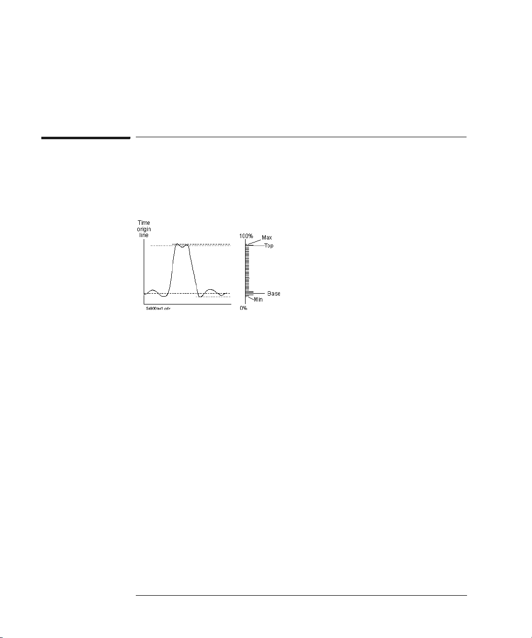
Chapter 1: Agilent Technologies 16533/34A Digitizing Oscilloscope
Automatic Measurements and Algorithms
“Increasing the Accuracy of Your Measurements” on page 73
“Autoscale” on page 32
How the Scope Makes Measurements
Automatic parametric measurements are calculated from a histogram.
Measurements are done as soon as valid data is available. The absolute
minimum and maximum are derived from the histogram.
Next, the statistical top and base values are calculated. The top 40% of
the histogram is scanned for the top value and the bottom 40% is
scanned for the base value. The center 20% of the histogram is not
scanned to prevent selecting the middle of a tri-state waveform.
The measurement algorithm decides whether the absolute maximum
and minimum values should be used, as in the case of triangle
waveforms, or the statistical top and base should be used, as in the case
of square waveforms.
After the top and base are calculated, the IEEE 10%, 50%, and 90%
thresholds are calculated. These thresholds determine edges and are
used by all timing measurements. For example, rise time is measured
from the lower threshold to the 90% threshold of a rising edge. Period,
frequency, and pulse width measurements use the 50% threshold.
Once the thresholds have been calculated, the edges can be
determined. A rising edge is defined as a transition that passes through
the 10%, 50%, and 90% threshold levels. A falling edge is defined as a
transition that passes through the 90%, 50%, and 10% threshold levels.
For an edge to be detected, it must complete the transition through all
62
Page 63

Chapter 1: Agilent Technologies 16533/34A Digitizing Oscilloscope
Automatic Measurements and Algorithms
three threshold levels.
Once the oscilloscope locates rising and falling edges, it calculates rise
time, fall time, and frequency. If too few sample points fall along an
edge, the measurement is not made. The oscilloscope ignores
incomplete transitions.
Average Voltage (Vavg)
Vavg is the average voltage of waveform data over the display. It does
not include data that is offscreen. The value is calculated by summing
all the data points on the screen and dividing by the number of them.
Period
Period is defined as the time between the 50% threshold crossings of
two consecutive, like-polarity edges.
The Agilent Technologies 16533A or 16534A Digitizing Oscilloscope
starts the measurement at the leftmost edge of the display.
Rise Time
Rise time is defined as the time at the 90% threshold minus the time at
the 10% threshold on the edge you are measuring.
63
Page 64
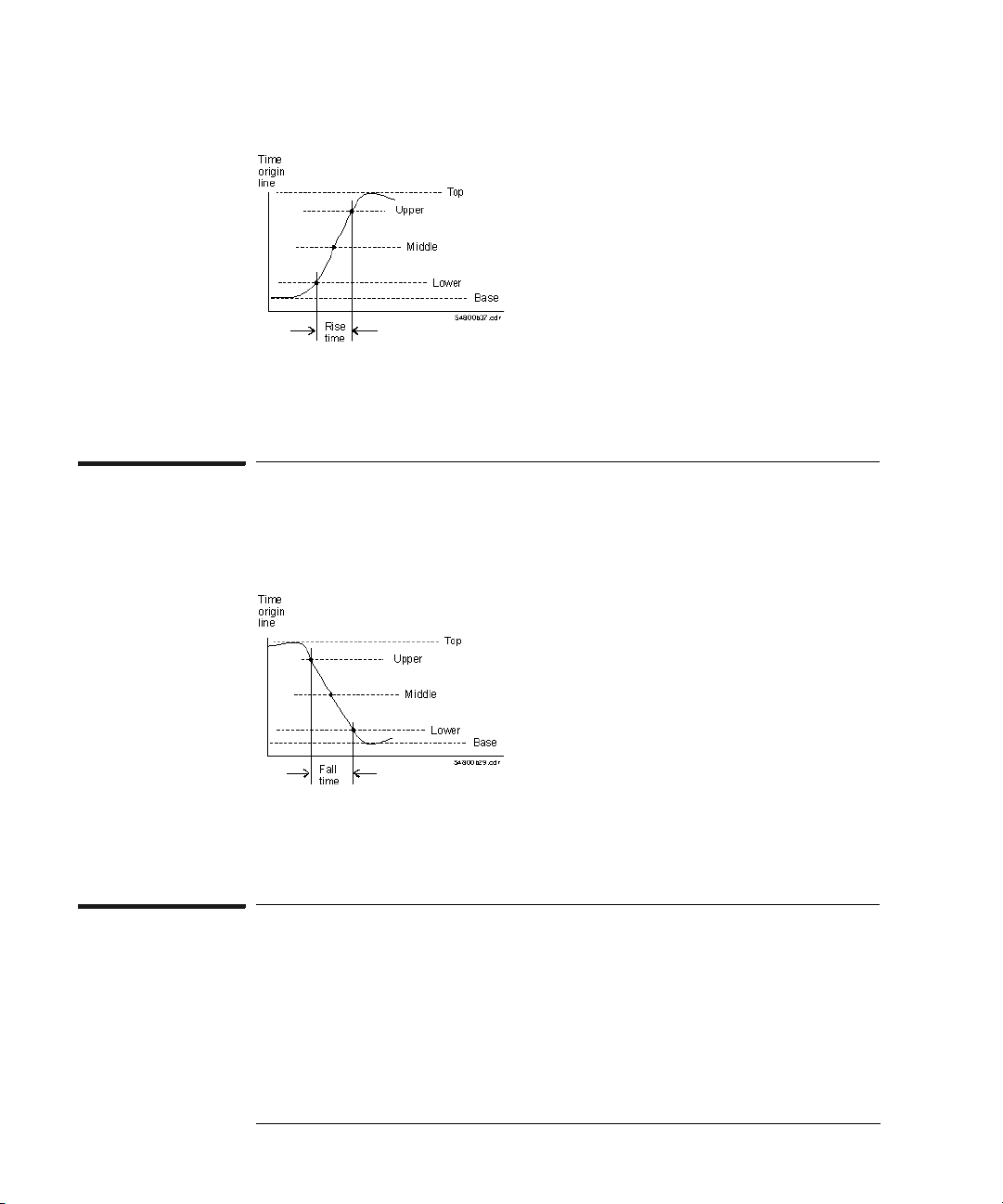
Chapter 1: Agilent Technologies 16533/34A Digitizing Oscilloscope
Automatic Measurements and Algorithms
The Agilent Technologies 16533A or 16534A Digitizing Oscilloscope
starts the measurement at the leftmost edge of the display.
Fall Time
Fall time is defined as the time at the 10% threshold minus the time at
the 90% threshold on the edge you are measuring.
The Agilent Technologies 16533A or 16534A Digitizing Oscilloscope
starts the measurement at the leftmost edge of the display.
Negative and Positive Pulse Width (±Width)
Negative pulse width is defined as the time from the 50% threshold of
the first falling edge to the 50% threshold of the next rising edge.
Positive pulse width is defined as the time from the 50% threshold of
the first rising edge to the 50% threshold of the next falling edge.
64
Page 65

Chapter 1: Agilent Technologies 16533/34A Digitizing Oscilloscope
Negative Pulse Width
Automatic Measurements and Algorithms
Positive Pulse Width
The Agilent Technologies 16533A or 16534A Digitizing Oscilloscope
starts the measurement at the leftmost edge of the display.
Frequency
Frequency is defined as 1/Period. Period is the time between the 50%
threshold crossings of two consecutive, like-polarity edges.
65
Page 66
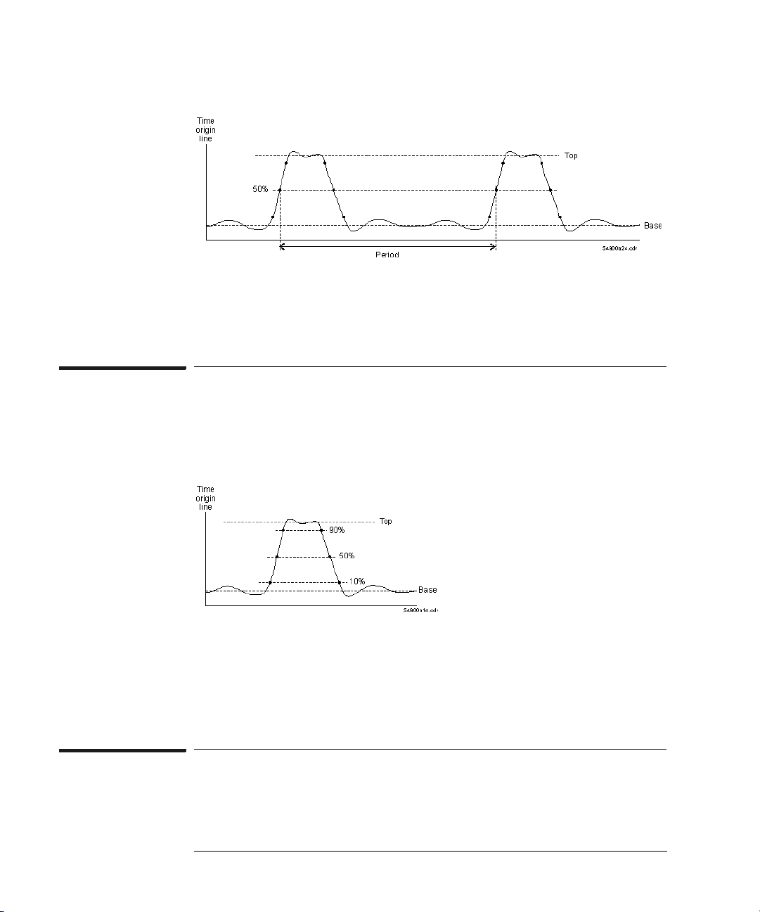
Chapter 1: Agilent Technologies 16533/34A Digitizing Oscilloscope
Automatic Measurements and Algorithms
The Agilent Technologies 16533A or 16534A Digitizing Oscilloscope
starts the measurement on the first edge of the leftmost portion of the
display.
Base Voltage (Vbase)
Vbase is the voltage of the statistical minimum level of the waveform
display, which is defined as the most frequently occurring voltage in
the histogram of the bottom 40% of the waveform.
Vbase may be equal to Vmin for many waveforms, such as triangle
waveforms. Similarly, Vtop may be equal to Vmax.
This measurement is position-independent and the entire display is
used for the measurement.
Top Voltage (Vtop)
Vtop is the voltage of the statistical maximum level of the waveform
66
Page 67
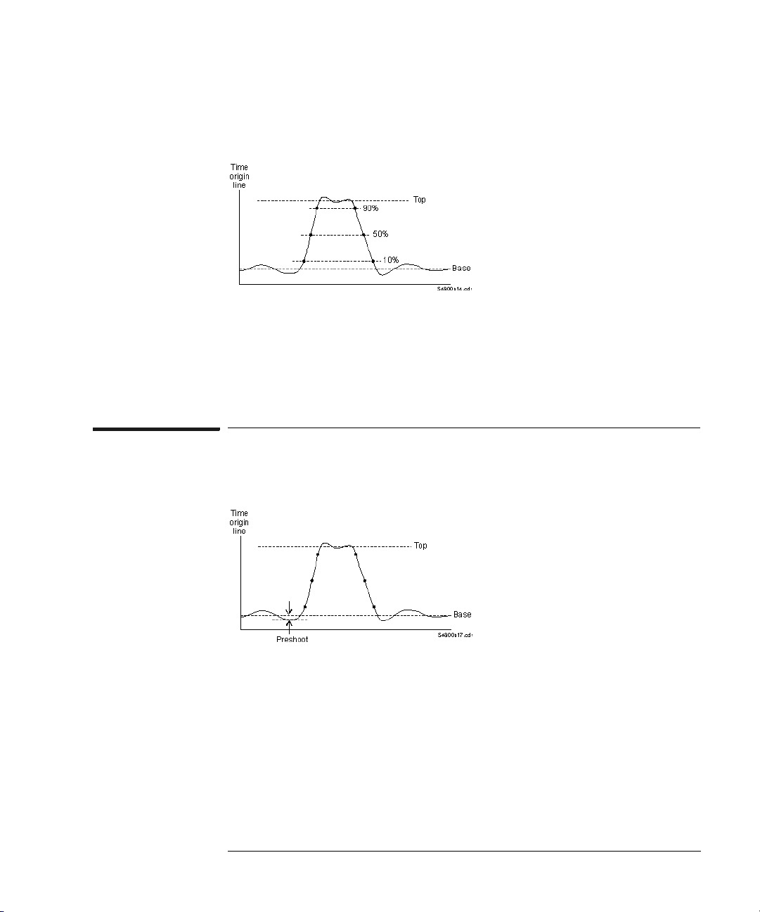
Chapter 1: Agilent Technologies 16533/34A Digitizing Oscilloscope
Automatic Measurements and Algorithms
display, which is defined as the most frequently occurring voltage in
the histogram of the top 40% of the waveform.
Vtop may be equal to Vmax for many waveforms, such as triangle
waveforms. Similarly, Vbase may be equal to Vmin.
This measurement is position-independent and the entire display is
used for the measurement.
Preshoot
Preshoot is a waveform distortion that precedes an edge transition.
If the edge is rising, preshoot will be 100*(base - local minimum)/ (top
- base). The local minimum is found half way from the 10% threshold
level to the 10% threshold level at the previous falling edge.
If the edge is falling, preshoot will be 100*(local maximum - top)/(top base). The local maximum is found half way from the 90% threshold
level to the previous 90% threshold level at the previous rising edge.
The Agilent Technologies 16533A or 16534A Digitizing Oscilloscope
starts the measurement at the first edge of the leftmost portion of the
67
Page 68

Chapter 1: Agilent Technologies 16533/34A Digitizing Oscilloscope
Automatic Measurements and Algorithms
display.
Overshoot
Overshoot is a waveform distortion that follows a major edge transition.
If the edge is rising, the overshoot will be 100*(local maximum - top)/
(top - base). The local maximum is found half way from the 90%
threshold level to the next 90% threshold level at the falling edge.
If the edge is falling, the overshoot will be 100*(base - local minimum)/
(top - base). The local minimum is found half way from the 10%
threshold level to the next 10% threshold level at the next rising edge.
The Agilent Technologies 16533A or 16534A Digitizing Oscilloscope
starts the measurement at the first edge on the leftmost portion of the
display.
Peak-to-Peak Voltage (Vpp)
Peak-to-peak voltage is defined as Vmax - Vmin. Vmax is the absolute
maximum voltage of the display. Vmin is the absolute minimum voltage
of the display.
68
Page 69

Chapter 1: Agilent Technologies 16533/34A Digitizing Oscilloscope
Automatic Measurements and Algorithms
This measurement is position-independent and the entire display is
used for the measurement.
Minimum Voltage (Vmin)
Vmin is the absolute minimum voltage of the waveform display.
This measurement is position-independent and the entire display is
used for the measurement.
Maximum Voltage (Vmax)
Vmax is the absolute maximum voltage of the waveform display.
69
Page 70

Chapter 1: Agilent Technologies 16533/34A Digitizing Oscilloscope
Automatic Measurements and Algorithms
This measurement is position-independent and the entire display is
used for the measurement.
Time of Minimum Voltage (Tmin)
Tmin is the first time that the minimum voltage occurs on the display.
This measurement is position-independent and the entire display is
used for the measurement.
Time of Maximum Voltage (Tmax)
Tmax is the first time that the maximum voltage occurs on the display.
This measurement is position-independent and the entire display is
used for the measurement.
Voltage Amplitude (Vamp)
Vamp is the amplitude of the waveform display. Vamp = Vtop - Vbase.
70
Page 71

Chapter 1: Agilent Technologies 16533/34A Digitizing Oscilloscope
Automatic Measurements and Algorithms
This measurement is position-independent and the entire display is
used for the measurement.
Vdcrms (Root Mean Square Voltage, DC)
Vdcrms is the root-mean-square voltage of the waveform. The equation
used is:
This measurement is position-independent and the entire display is
used for the measurement. Data points offscreen are not included.
About the Measurements
The Agilent Technologies 16533A or 16534A Digitizing Oscilloscope
makes measurements after every trigger event, always maintaining
continuity between the measurement results and the oscilloscope
display. This makes sure that no aberration in the waveform under
observation is missed.
If the waveform is clipped, the oscilloscope cannot make some
automatic measurements. These measurements will show clipped
where a value would normally appear. Other indicators you may see
are:
71
Page 72

Chapter 1: Agilent Technologies 16533/34A Digitizing Oscilloscope
Automatic Measurements and Algorithms
? Value is questionable. This can occur because the signal is
clipped, there are not enough points, or the amplitude is
too small.
< The result is less than or equal to the value shown. This can
occur when the waveform is clipped low or not enough
points are available.
> The result is greater than or equal to the value shown. This
can occur when the waveform is clipped high or not enough
points are available.
(blank) No value could be calculated. The most common reason is
missing edges, such as when the display shows less than a
full period of a waveform.
The Agilent Technologies 16533A or 16534A will interpolate sample
points if necessary to determine pulse parameters for automatic
measurements. Excessive interpolation can lead to jitter on
measurements; if this occurs you may have to increase the sample rate.
By default, the oscilloscope uses the IEEE thresholds of 10, 50, and 90
percent for pulse measurements. A rising or falling edge is only
recognized after passing through all three thresholds. These thresholds
appear on the example pulse waveform as shown below:
Period and Frequency Measurements
At least one full cycle of the waveform with at least two like edges must
be displayed for period and frequency measurements. Automatic
waveform measurements use a single pulse and may have significant
errors introduced by interpolation and trigger inaccuracies. The
leftmost cycle is used for making measurements.
72
Page 73

Chapter 1: Agilent Technologies 16533/34A Digitizing Oscilloscope
Automatic Measurements and Algorithms
Pulse Width Measurements
For either the -Width or +Width measurements, a complete pulse must
be displayed to make a valid measurement. Remember that an edge
must pass through all three thresholds to be recognized as an edge.
Therefore, it is important that the pulse be positioned so that both
pulse edges transition through all three thresholds and are displayed
on the screen. Pulse width is measured from the leftmost valid edge to
the next valid edge.
Rise Time, Fall Time, Preshoot, and Overshoot Measurements
The leading, rising edge of the waveform must be displayed for rise
time and rising edge preshoot and overshoot measurements. The
trailing, falling edge of the waveform must be displayed for fall time
and falling edge preshoot and overshoot measurements. The leftmost
edge is used for measurements.
Remember that an edge must pass through all three thresholds to be
recognized as an edge. Therefore, it is important that the pulse be
positioned so that all three thresholds are displayed on the screen. Rise
time, fall time, preshoot, and overshoot measurements will be more
accurate if you expand the edge of the waveform by choosing a faster
sweep speed. Expanding the waveform will provide more data points
on an edge, reduce interpolation, and thus provide a more accurate
measurement.
Increasing the Accuracy of Your Measurements
Things you can do to make your measurements more accurate:
• Deskew the oscilloscope channels.
To deskew the oscilloscope channels, perform the Channel Skew
procedure as part of calibrating the oscilloscope (see page 10).
• Use automatic measurements where possible.
• For positive and negative pulse width, make sure enough top and bottom
voltages are showing to accurately calculate the top and base voltages.
• When using markers, increase the sampling rate.
73
Page 74

Chapter 1: Agilent Technologies 16533/34A Digitizing Oscilloscope
Automatic Measurements and Algorithms
• Minimize the effect of DC errors on time measurements by
• measuring between identical edges (same slew rate, amplitude and
offset).
• using the same DC level to reference each endpoint of the interval.
• performing the measurement on the fastest-slewing portion of each
edge.
• making the waveform as large as possible.
• Calibrate (see page 10) your oscilloscope after it has warmed up.
See Also “Getting a Stable Trigger” on page 43
74
Page 75

Chapter 1: Agilent Technologies 16533/34A Digitizing Oscilloscope
Using Markers
Using Markers
The Agilent Technologies 16533A or 16534A Digitizing Oscilloscope
has both local and global markers. The local markers can only be used
within the oscilloscope window. The global markers retain their
position across the data sets of all instruments that are part of the same
group run as the oscilloscope.
The global markers are G1 and G2 and only measure time. The local
markers consist of four voltage markers, V1 - V4, and two time
markers, T1 and T2.
To access the markers, select the Markers tab then select the Setup...
button. The Marker Setup dialog appears, from which you can turn on
any of the markers by selecting the appropriate button. From this
dialog, you can also change the channel of the voltage markers.
The information after this does not apply to automatic time markers.
Those are covered in a separate topic listed below.
When the markers are turned on, you can set their values by dragging
them. If a marker moves offscreen because of scrolling or from typing
in a value in the Marker Setup window, you can return it to the edge of
the display by selecting the arrow buttons in the Marker Setup window.
You can also place markers by selecting the area you want the marker
on and choosing Place Marker and the marker you want from the
menu. If your cursor is on a marker already, select Markers... to display
the Marker Setup dialog.
See Also “What Do the Display Symbols Mean?” on page 57
“About Automatic Time Markers” on page 76
Working with Global Markers in Correlated Displays (see the Markers help
volume)
75
Page 76

Chapter 1: Agilent Technologies 16533/34A Digitizing Oscilloscope
Using Markers
About Automatic Time Markers
Automatic time markers indicate the time at which a specified voltage
crossing occurs. For instance, if you scroll the display, an automatic
time marker defined for the third edge will automatically reposition
itself on the edge third from the left. A regular time marker would
remain placed on the waveform and scroll with it off the display.
When you turn on an automatic time marker, Min T2-T1, Max T2-T1,
and Mean T2-T1 appear at the bottom of the Markers area. You can
gather statistics as long as both time markers are on, and one is an
automatic marker. Changing any part of the display will clear statistics.
To turn on automatic time markers
1. Under the Markers tab, select the Setup... button.
2. Select the time marker button.
3. Choose Marker [OFF] to turn on the marker.
4. Choose Automatic [OFF] to put it in automatic mode.
5. Select the Define Automatic Marker... button.
If you did not put the marker in automatic mode, the area to the right of
T1 or T2 is a time from trigger setting.
6. Specify the automatic setting. Percentage level is based on the
automatically calculated top and base voltage.
Automatic time markers cannot be dragged when they are on their
specified edge. If the specified edge does not exist, they can be
dragged like regular time markers.
See Also “Top Voltage (Vtop)” on page 66
“Base Voltage (Vbase)” on page 66
“How the Scope Makes Measurements” on page 62
76
Page 77

Chapter 1: Agilent Technologies 16533/34A Digitizing Oscilloscope
Differences from a Standard Digitizing Oscilloscope
Differences from a Standard Digitizing
Oscilloscope
There are some differences between an Agilent Technologies 16533A
or 16534A Digitizing Oscilloscope and a standard stand-alone digitizing
oscilloscope.
• Clipped data (data that is offscreen at acquisition) stays at the top or
bottom edge of the display area when the clipped waveform is resized or
has the offset moved. The waveform appears to have a gap in it where the
clipped data was.
• Repetitive run is repetitive real-time acquisitions, not what is also referred
to as equivalent-time mode.
• When there are not enough data points to map at least one sample to each
column of pixels in the display, the sin(x)/x interpolation filter is on. You
cannot turn it off.
• There is only one graticule area. All oscilloscope channels are sampled and
displayed at the same rate.
• The Agilent Technologies 16533A or 16534A oscilloscope is easier to use in
conjunction with a logic analyzer because arming is handled by the Agilent
Technologies 16700A/B-series frame. You do not need to connect any wires
between the two modules.
77
Page 78

Chapter 1: Agilent Technologies 16533/34A Digitizing Oscilloscope
Using Waveform Memories
Using Waveform Memories
The four waveform memories store copies of waveforms for display
within the oscilloscope tool. The memories cannot be exported to other
display tools.
To Use Waveform Memory
This procedure assumes you already have acquired a waveform that
you want to store.
1. Under the Memories tab, select the Setup... button.
2. In the Load Waveform area, select the waveform source.
The button text depends on your setup, but the default is channel 1.
3. Select the Load button.
Sources can be any channel or another waveform memory. If the source
does not contain any data (for example, the channel was off during the last
acquisition), "Waveform data is not valid!" appears briefly at the top of the
Waveform Memory Setup window. If the display is set to accumulate or
average, only the last acquired waveform is loaded.
4. To view the memory, select the Off radio button.
5. To make the memory display independent of the main display controls,
select the box to the left of Horizontal. This enables the independent
horizontal scale controls.
Waveform memories are erased between sessions. They are not
cleared when the display is cleared. In all other ways, waveform
memories are treated like channels by the display functions.
78
Page 79

Chapter 1: Agilent Technologies 16533/34A Digitizing Oscilloscope
Loading and Saving Oscilloscope Configurations
Loading and Saving Oscilloscope
Configurations
Oscilloscope settings and data can be saved to a configuration file. You
can also save any tools connected to the oscilloscope. Later, you can
restore your data and settings by loading the configuration file into the
oscilloscope.
• Loading Configuration Files (see the Agilent Technologies 16700A/B-
Series Logic Analysis System help volume)
• Saving Configuration Files (see the Agilent Technologies 16700A/B-
Series Logic Analysis System help volume)
79
Page 80

Chapter 1: Agilent Technologies 16533/34A Digitizing Oscilloscope
When Something Goes Wrong
When Something Goes Wrong
•“Error Messages” on page 80
•“Calibration Problems” on page 80
•“Triggering Problems” on page 80
•“Other Problems” on page 81
Error Messages
• No valid signals have been found. (see page 82)
• Incorrect Calibration Factors for this software revision. (see page 83)
• Waiting for IMB Arm. (see page 83)
Calibration Problems
Calibration is not possible because NV RAM is protected
Unprotect the NV RAM and try again.
Calibration Procedure did not complete successfully
The Calibration window shows which tests passed and failed. If any test
failed and all cables were correctly hooked up, you should contact your
Agilent Technologies Service Center.
Triggering Problems
Scope loses trigger when changes made to offset
The trigger level may be too high or too low to reliably trigger before
autotrigger. Sometimes this over-sensitivity to offset is caused by too
80
Page 81

Chapter 1: Agilent Technologies 16533/34A Digitizing Oscilloscope
When Something Goes Wrong
high an attenuation factor in the channel setup.
Low frequency waveform appears to have unstable trigger
See “Getting a Stable Trigger” on page 43.
Nothing happening
If the scope is being triggered by another instrument, and you were
changing some settings, the scope may have missed its trigger signal.
The other common causes when the trigger is set to Triggered are
• trigger level occurs outside normal signal
• the oscilloscope is waiting for a rare event
You can either stop the oscilloscope or set the trigger to Auto to look
for these conditions.
Other Problems
Autoscale failed to find a waveform
Check that either channel 1 or channel 2 is on. Autoscale autoscales all
channels, but can only trigger on channel 1 or 2.
Also check for correct channel setup. The wrong setup can attenuate a
proper signal into an apparent DC signal.
Waveform has gaps when offset is changed or V/div increased
If a waveform is clipped, when you move the offset the clipped portion
of the waveform will stay at the top or bottom of the display, with a
break in the rest of the waveform. This also happens if you increase V/
div so that more of the waveform fits in the display. Those portions that
were off the display during acquisition contain uncertain data and so
are not displayable.
To get good data, make the changes to your settings and run again.
81
Page 82

Chapter 1: Agilent Technologies 16533/34A Digitizing Oscilloscope
When Something Goes Wrong
Trigger won’t return to center
The trigger delay is affected by both the scrollbar position and the
value in the delay field. To re-center the trigger in the acquisition,
1. Drag the scrollbar to the center of the scroll area. There is a slight delay in
movement when the bar is at the center.
2. Set Delay at the bottom of the window to 0 seconds, and press enter.
The scrollbar may jump away from the center. Do not reset it.
3. Select the Run button to get a new acquisition.
The trigger is now in the center of the acquisition as well as the display
window.
Scope keeps stopping
The Agilent Technologies 16533A or 16534A Digitizing Oscilloscope
default to single-shot acquisition. To have the oscilloscope keep
running, select the Run Repetitive button.
NOTE: The Agilent Technologies 16533A or 16534A Digitizing Oscilloscope does not
do equivalent-time sampling. All runs in the repetitive run mode are single
acquisitions.
Scope locked up
The logic analysis system may be busy. Wait a few minutes and try
again. If the problem persists, exit the session and cycle power on the
frame.
If you can find a sequence of steps that always or frequently causes this
to happen, please contact the Agilent Technologies Sales Office to
report this bug.
Error Message: No Valid Signals
This message only comes up when autoscale is run and the oscilloscope
is unable to detect any line activity. Possible causes are:
• No channels are turned on. Autoscale does not check channels that are
turned off.
82
Page 83

Chapter 1: Agilent Technologies 16533/34A Digitizing Oscilloscope
When Something Goes Wrong
• The oscilloscope board is damaged. Run calibration to check for signal
detection.
Autoscale does detect flat, dc signals so that is not a cause.
Error Message: Incorrect Calibration Factors
This message appears when you have upgraded your oscilloscope
software, but not re-calibrated the Agilent Technologies 16533A or
16534A oscilloscope.
See the Logic Analysis System Installation Guide or “Calibrating the
Oscilloscope” on page 10 for instructions on calibrating the
oscilloscope.
Status Message: Waiting for IMB Arm
This message appears when the oscilloscope is being triggered by
another instrument in the logic analysis system. The instrument that
will trigger the oscilloscope has not yet found its own trigger, and
therefore hasn't sent the IMB Arm signal to the oscilloscope.
If the other instrument has already triggered, perform the Self Test
(see page 83) on the oscilloscope. If any of the tests fail, contact your
Agilent Technologies Sales Office for service.
Performing the Self Tests. To verify that the oscilloscope hardware
is operational, run the Self Test utility. The Self Tst function of the logic
analysis system performs functional tests on both the system and any
installed modules.
NOTE: The operational accuracy calibration requires that the oscilloscope hardware
meets specifications. The self test only requires that the hardware function.
An oscilloscope can pass self-test and still fail calibration.
To Run the Self-Test Utility
1. If you have any work in progress, save it to a configuration file. (see the
Agilent Technologies 16700A/B-Series Logic Analysis System help
volume)
83
Page 84

Chapter 1: Agilent Technologies 16533/34A Digitizing Oscilloscope
When Something Goes Wrong
2. From the system window, select the System Administration toolbar
button.
3. Select the Admin tab, then select the Self Test... button.
The system closes all windows before starting up Self Test.
4. Select Master Frame.
If the module is in an expansion frame, select Expansion Frame.
5. Select the oscilloscope.
6. In the Self Test dialog box, select Te s t A l l .
You can also run individual tests by selecting them. Tests that require you
to do something must be run this way.
If any test fails, contact your local Agilent Technologies Sales Office or
Service Center for assistance.
84
Page 85

Chapter 1: Agilent Technologies 16533/34A Digitizing Oscilloscope
Specifications and Characteristics
Specifications and Characteristics
NOTE: Specifications are valid after a 30 minute warm-up period, and within 10 °C
from the firmware calibration temperature.
NOTE: Definition of Terms
To understand the difference between specifications (see page 88) and
characteristics (see page 88), and what gets a calibration procedure (see
page 88) and what gets a function test (see page 89), refer to appropriate
links within this note.
• Specifications (see page 85)
• Operating Environment (see page 85)
• Characteristics (see page 86)
Specifications
Note: Specifications refer to the input to the BNC connector.
Bandwidth
16533A dc to 250 MHz
16534A dc to 500 MHz
dc offset accuracy +/- (1% of offset + 2% of full scale)
dc voltage measurement accuracy +/- (1.25% of full scale + offset accuracy
+ 0.016 div)
Time interval measurement accuracy +/- [(0.005% of delta T) + (2e-6 x delay
setting)
at maximum sampling rate, on a + 100 ps]
single card, on a single acquisition
Trigger sensitivity from 10 mV/div to 10 V/div
dc to 50 MHz 0.25 div
50 MHz to 500 MHz 0.5 div
Trigger sensitivity at 4 mV/div
dc to 50 MHz 0.63 div
50 MHz to 500 MHz 1.25 div
Input resistance 1 Mohm +/- 1%
50 ohm +/- 1%
85
Page 86

Chapter 1: Agilent Technologies 16533/34A Digitizing Oscilloscope
Specifications and Characteristics
Operating
Environment
Characteristics
Power Requirements
All power supplies required for operating the oscilloscope are
supplied through the backplane connector in the logic analysis system.
Operating Environment Characteristics
The oscilloscope module’s reliability is enhanced when operating
the module within the following ranges:
- Indoor use only.
- Temperature: +20 degrees C to +35 degrees C
(+68 degrees F to +95 degrees F)
- Humidity: 20% to 80% noncondensing
General
Maximum sampling rate
16533A 1 GSa/S
16534A 2 GSa/S
Number of channels 2 to 8 channels using the same timebase
and trigger.
Waveform record length 32768 points
Vertical (Voltage)
(characteristics refer to the input at the BNC connector)
Vertical sensitivity range 4 mV/div to 10 V/div in 1:2:4 steps
Vertical resolution 8 bits over 4 vertical divisions
Rise time (calculated from
bandwidth)
16533A 1.4 ns
16534A 700 ps
dc gain accuracy +/- (1.25% of full scale + 0.08% per degree C
difference from calibration temperature)
dc offset range (1:1 probe)
Vertical sensitivity Offset range
4 mV/div - 100 mV/div +/- 2 V
100 mV/div - 400 mV/div +/- 10 V
400 mV/div - 2.5 V/div +/- 50 V
2.5 V/div - 10 V/div +/- 250 V
Probe attenuation Any ratio from 1:1 to 1000:1 factor
Channel-to-channel isolation (with channel sensitivities equal)
dc to 50 MHz 40 dB
50 MHz to 250 MHz (16533A) 30 dB
50 MHz to 500 MHz (16534A) 30 dB
Maximum safe input voltage
1 Mohm +/- 250 Vdc + peak ac (&<10KHz), CAT I
50 ohm 5 Vrms, CAT I
86
Page 87

Chapter 1: Agilent Technologies 16533/34A Digitizing Oscilloscope
Specifications and Characteristics
Input coupling
1 Mohm ac, dc
50 ohm dc only
Input C approximately 7 pF
Number of channels: 2,4,6, or 8 simultaneous channels using the same
trigger OR up to 10 channels with independent triggers for each pair
of channels. Maximum of 20 channels with Agilent Technologies 16701A expansion
frame.
Horizontal (Time)
Timebase ranges 0.5 ns/div to 5 s/div
Timebase resolution 10 ps
Delay range, pre-trigger 81.8 s, 5 divisions
Delay range, post-trigger 2.5e3 seconds
Time interval measurement accuracy +/- [(0.005% of delta T) + (2e-6 x delay
setting)
for sampling rates other than + (0.15/sample rate)]
maximum, for bandwidth-limited
signals (signal rise time
> 1.4/sample rate) on a single card,
on a single acquisition
Time interval measurement accuracy +/- [(0.005% of delta T) + (2e-6 x delay
setting)
for 2, 3, or 4 cards operation on + 550 ps]
a single timebase, for measurements
made between channels on different
cards, at maximum sampling rate
Tr ig ge r
Trigger level range Within display window (vertical offset
+/- 2 divisions)
Immediate trigger mode Triggers immediately after arming
condition is met
Edge trigger mode Triggers on rising or falling edge on
channel 1 or channel 2
Pattern trigger mode Triggers on entering or exiting a
specified pattern across both channels
Auto condition trigger mode Self-triggers if trigger is not satisfied
within approximately 100 ms after arming
Events delay trigger mode The trigger can be set to occur on the
nth occurrence of an edge or pattern,
n <= 32000
Intermodule trigger mode Arms another measurement module or acti vates a trigger output on the rear panel
BNC connector when the trigger condition
is met
87
Page 88

Chapter 1: Agilent Technologies 16533/34A Digitizing Oscilloscope
Specifications and Characteristics
What is a Specification
A Specification is a numeric value, or range of values, that bounds the
performance of a product parameter. The product warranty covers the
performance of parameters described by specifications. Products
shipped from the factory meet all specifications. Additionally, the
products sent to Agilent Technologies Customer Service Centers for
calibration and returned to the customer meet all specifications.
Specifications are verified by Calibration Procedures.
What is a Characteristic
Characteristics describe product performance that is useful in the
application of the product, but that is not covered by the product
warranty. Characteristics describe performance that is typical of the
majority of a given product, but not subject to the same rigor
associated with specifications.
Characteristics are verified by Function Tests.
What is a Calibration Procedure
Calibration procedures verify that products or systems operate within
the specifications. Parameters covered by specifications have a
corresponding calibration procedure. Calibration procedures include
both performance tests and system verification procedure. Calibration
procedures are traceable and must specify adequate calibration
standards.
Calibration procedures verify products meet the specifications by
comparing measured parameters against a pass-fail limit. The pass-fail
limit is the specification less any required guardband.
The term "calibration" refers to the process of measuring parameters
and referencing the measurement to a calibration standard rather than
88
Page 89

Chapter 1: Agilent Technologies 16533/34A Digitizing Oscilloscope
Specifications and Characteristics
the process of adjusting products for optimal performance, which is
referred to as an "operational accuracy calibration".
What is a Function Test
Function tests are quick tests designed to verify basic operation of a
product. Function tests include operator’s checks and operation
verification procedures. An operator’s check is normally a fast test
used to verify basic operation of a product. An operation verification
procedure verifies some, but not all, specifications, and often at a lower
confidence level than a calibration procedure.
89
Page 90
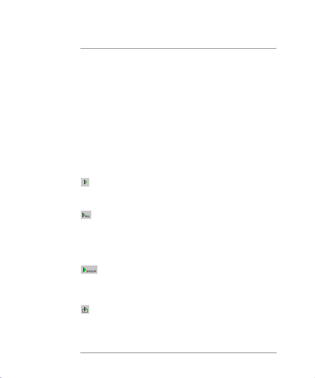
Chapter 1: Agilent Technologies 16533/34A Digitizing Oscilloscope
Run/Group Run Function
Run/Group Run Function
Using Run - Run All - Group Run
The Run/Stop functions are initiated by selecting icons in the icon bar
at the top of the tool windows. All instrument, display, and analysis tool
windows will have one of the Run icons shown below to initiate the run
function.
When two or more instrument tools are configured, they can be run
either independently or as a group. If run in a group, it is called an
Intermodule measurement. Use the Intermodule Window (see the
Agilent Technologies 16700A/B-Series Logic Analysis System help
volume) to coordinate the arming in a "Group Run". A common "Group
Run" configuration is to configure one instrument to trigger and then
arm another instrument to start evaluation of its own trigger condition.
The Run Single icon appears if you have a single instrument
configured in your measurement and you want to run a single
acquisition.
The Run All icon always appears in the System, Workspace and
Run Status windows. Also appears in instrument and display windows
when you are using multiple instruments in your measurement and
these instruments ARE NOT configured in an intermodule
measurement (Group Run). This choice runs a single acquisition on all
instruments in the configuration.
The Group Run icon appears in all windows when you are using
multiple instruments, and these instruments are configured into a
Group Run. This choice runs a single acquisition on all instruments in
the Group Run configuration.
The Run Repetitive icon appears in all windows. It is used to run a
Run Single, Run All, and a Group Run acquisition repetitively. The
current run mode will continue to run until Cancel is selected.
90
Page 91
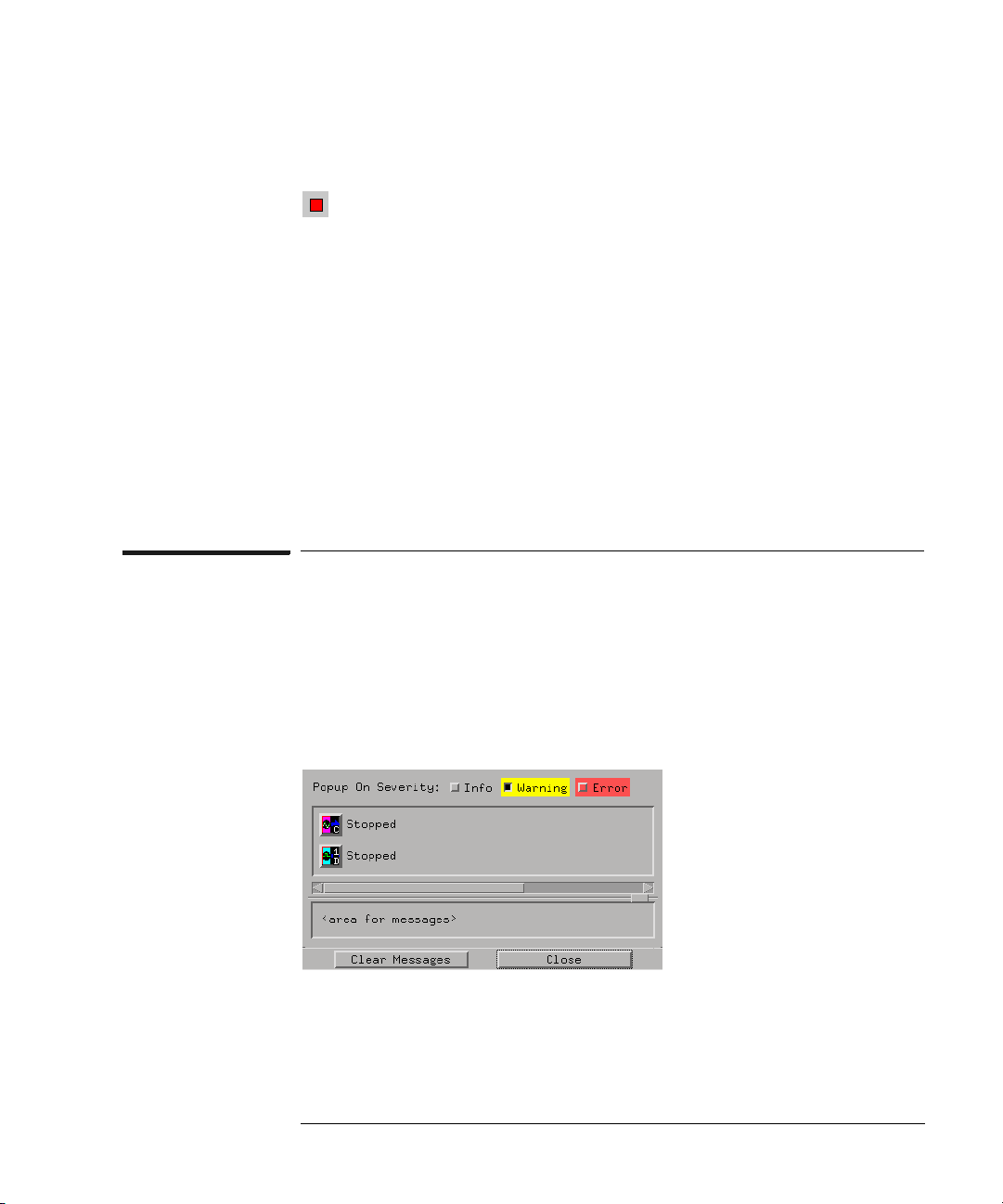
Chapter 1: Agilent Technologies 16533/34A Digitizing Oscilloscope
Run/Group Run Function
Using Stop
The Stop icon terminates all of the run functions shown above.
• Stops a single instrument running a measurement (perhaps waiting for a
trigger condition).
• Stops all instruments running separate measurements (easily viewed from
the Workspace window).
• Stops all instruments running in a Group Run configuration.
See Also
“Demand Driven Data” on page 92
“Checking Run Status” on page 91
Checking Run Status
The Run Status dialog provides status information about the currently
configured instruments, and the status of the run with respect to the
trigger specification.
To access the Run Status dialog, select the Run Status icon in the
System Window, or, select Window -> System -> Run Status
91
Page 92

Chapter 1: Agilent Technologies 16533/34A Digitizing Oscilloscope
Run/Group Run Function
Demand Driven Data
When an analyzer measurement occurs, acquisition memory is filled
with data that is then transferred to the display memory of the analysis
or display tools you are using, as needed by those tools. In normal use,
this demand driven data approach saves time by not transferring
unnecessary data.
Since acquisition memory is cleared at the beginning of a
measurement, stopping a run may create a discrepancy between
acquisition memory and the memory buffer of connected tools. Without
a complete trace of acquisition memory, the display memory will
appear to have ’holes’ in it which appear as filtered data.
This situation will occur in these cases:
• If you stop a repetitive measurement after analyzer data has been cleared
and before the measurement is complete.
• If a trigger is not found by the analyzer and the run must be stopped to
regain control.
To make sure all of the data in a repetitive run is available for viewing:
• In the workspace, attach a Filter tool to the output of the analyzer.
• In the Filter, select "Pass Matching Data"
• In the filter terms, assure the default pattern of all "Don't Cares" (Xs).
This configuration will always transfer all data from acquisition
memory. While this configuration will increase the time of each run, it
will guarantee that repetitive run data is available regardless of when it
is stopped.
92
Page 93

Glossary
absolute Denotes the time period
or count of states between a captured
state and the trigger state. An
absolute count of -10 indicates the
state was captured ten states before
the trigger state was captured.
acquisition Denotes one complete
cycle of data gathering by a
measurement module. For example,
if you are using an analyzer with
128K memory depth, one complete
acquisition will capture and store
128K states in acquisition memory.
analysis probe A probe connected
to a microprocessor or standard bus
in the device under test. An analysis
probe provides an interface between
the signals of the microprocessor or
standard bus and the inputs of the
logic analyzer. Also called a
preprocessor.
analyzer 1 In a logic analyzer with
two machines, refers to the machine
that is on by default. The default
name is Analyzer<N>, where N is
the slot letter.
analyzer 2 In a logic analyzer with
two machines, refers to the machine
that is off by default. The default
name is Analyzer<N2>, where N is
the slot letter.
armed before it can search for its
trigger condition. Typically,
instruments are armed immediately
when Run or Group Run is selected.
You can set up one instrument to arm
another using the Intermodule
Window. In these setups, the second
instrument cannot search for its
trigger condition until it receives the
arming signal from the first
instrument. In some analyzer
instruments, you can set up one
analyzer machine to arm the other
analyzer machine in the Trigger
Window.
asterisk (*) See edge terms,
glitch, and labels.
bits Bits represent the physical logic
analyzer channels. A bit is a channel
that has or can be assigned to a label.
A bit is also a position in a label.
card This refers to a single
instrument intended for use in the
Agilent Technologies 16600A-series
or 16700A/B-series mainframes. One
card fills one slot in the mainframe. A
module may comprise a single card or
multiple cards cabled together.
channel The entire signal path from
the probe tip, through the cable and
module, up to the label grouping.
arming An instrument tool must be
93
click When using a mouse as the
Page 94

Glossary
pointing device, to click an item,
position the cursor over the item.
Then quickly press and release the
left mouse button.
clock channel A logic analyzer
channel that can be used to carry the
clock signal. When it is not needed
for clock signals, it can be used as a
data channel, except in the Agilent
Technologies 16517A.
context record A context record is
a small segment of analyzer memory
that stores an event of interest along
with the states that immediately
preceded it and the states that
immediately followed it.
context store If your analyzer can
perform context store
measurements, you will see a button
labeled Context Store under the
Trigger tab. Typical context store
measurements are used to capture
writes to a variable or calls to a
subroutine, along with the activity
preceding and following the events. A
context store measurement divides
analyzer memory into a series of
context records. If you have a 64K
analyzer memory and select a 16state context, the analyzer memory is
divided into 4K 16-state context
records. If you have a 64K analyzer
memory and select a 64-state
context, the analyzer memory will be
divided into 1K 64-state records.
count The count function records
periods of time or numbers of state
transactions between states stored in
memory. You can set up the analyzer
count function to count occurrences
of a selected event during the trace,
such as counting how many times a
variable is read between each of the
writes to the variable. The analyzer
can also be set up to count elapsed
time, such as counting the time spent
executing within a particular function
during a run of your target program.
cross triggering Using intermodule
capabilities to have measurement
modules trigger each other. For
example, you can have an external
instrument arm a logic analyzer,
which subsequently triggers an
oscilloscope when it finds the trigger
state.
data channel A channel that
carries data. Data channels cannot be
used to clock logic analyzers.
data field A data field in the pattern
generator is the data value associated
with a single label within a particular
data vector.
data set A data set is made up of all
labels and data stored in memory of
any single analyzer machine or
94
Page 95

Glossary
instrument tool. Multiple data sets
can be displayed together when
sourced into a single display tool. The
Filter tool is used to pass on partial
data sets to analysis or display tools.
debug mode See monitor.
delay The delay function sets the
horizontal position of the waveform
on the screen for the oscilloscope and
timing analyzer. Delay time is
measured from the trigger point in
seconds or states.
demo mode An emulation control
session which is not connected to a
real target system. All windows can
be viewed, but the data displayed is
simulated. To start demo mode,
select Start User Session from the
Emulation Control Interface and
enter the demo name in the
Processor Probe LAN Name field.
Select the Help button in the Start
User Session window for details.
device under test The system
under test, which contains the
circuitry you are probing. Also known
as a target system.
don’t care For terms, a "don’t care"
means that the state of the signal
(high or low) is not relevant to the
measurement. The analyzer ignores
the state of this signal when
determining whether a match occurs
on an input label. "Don’t care" signals
are still sampled and their values can
be displayed with the rest of the data.
Don’t cares are represented by the X
character in numeric values and the
dot (.) in timing edge specifications.
dot (.) See edge terms, glitch,
labels, and don’t care.
double-click When using a mouse
as the pointing device, to double-click
an item, position the cursor over the
item, and then quickly press and
release the left mouse button twice.
deskewing To cancel or nullify the
effects of differences between two
different internal delay paths for a
signal. Deskewing is normally done
by routing a single test signal to the
inputs of two different modules, then
adjusting the Intermodule Skew so
that both modules recognize the
signal at the same time.
95
drag and drop Using a Mouse:
Position the cursor over the item, and
then press and hold the left mouse
button. While holding the left mouse
button down, move the mouse to
drag the item to a new location. When
the item is positioned where you
want it, release the mouse button.
Page 96

Glossary
Using the Touchscreen:
Position your finger over the item,
then press and hold finger to the
screen. While holding the finger
down, slide the finger along the
screen dragging the item to a new
location. When the item is positioned
where you want it, release your
finger.
edge mode In an oscilloscope, this
is the trigger mode that causes a
trigger based on a single channel
edge, either rising or falling.
edge terms Logic analyzer trigger
resources that allow detection of
transitions on a signal. An edge term
can be set to detect a rising edge,
falling edge, or either edge. Some
logic analyzers can also detect no
edge or a glitch on an input signal.
Edges are specified by selecting
arrows. The dot (.) ignores the bit.
The asterisk (*) specifies a glitch on
the bit.
emulation module A module
within the logic analysis system
mainframe that provides an
emulation connection to the debug
port of a microprocessor. An E5901A
emulation module is used with a
target interface module (TIM) or an
analysis probe. An E5901B emulation
module is used with an E5900A
emulation probe.
emulation probe The stand-alone
equivalent of an emulation module.
Most of the tasks which can be
performed using an emulation
module can also be performed using
an emulation probe connected to
your logic analysis system via a LAN.
emulator An emulation module or
an emulation probe.
Ethernet address See link-level
address.
events Events are the things you
are looking for in your target system.
In the logic analyzer interface, they
take a single line. Examples of events
are Label1 = XX and Timer 1 > 400
ns.
filter expression The filter
expression is the logical OR
combination of all of the filter terms.
States in your data that match the
filter expression can be filtered out or
passed through the Pattern Filter.
filter term A variable that you
define in order to specify which
states to filter out or pass through.
Filter terms are logically OR’ed
together to create the filter
expression.
Format The selections under the
logic analyzer Format tab tell the
96
Page 97

Glossary
logic analyzer what data you want to
collect, such as which channels
represent buses (labels) and what
logic threshold your signals use.
frame The Agilent Technologies
16600A-series or 16700A/B-series
logic analysis system mainframe. See
also logic analysis system.
gateway address An IP address
entered in integer dot notation. The
default gateway address is 0.0.0.0,
which allows all connections on the
local network or subnet. If
connections are to be made across
networks or subnets, this address
must be set to the address of the
gateway machine.
glitch A glitch occurs when two or
more transitions cross the logic
threshold between consecutive
timing analyzer samples. You can
specify glitch detection by choosing
the asterisk (*) for edge terms under
the timing analyzer Trigger tab.
grouped event A grouped event is
a list of events that you have
grouped, and optionally named. It can
be reused in other trigger sequence
levels. Only available in Agilent
Technologies 16715A, 16716A, and
16717A logic analyzers.
held value A value that is held until
the next sample. A held value can
exist in multiple data sets.
immediate mode In an
oscilloscope, the trigger mode that
does not require a specific trigger
condition such as an edge or a
pattern. Use immediate mode when
the oscilloscope is armed by another
instrument.
interconnect cable Short name for
module/probe interconnect cable.
intermodule bus The intermodule
bus (IMB) is a bus in the frame that
allows the measurement modules to
communicate with each other. Using
the IMB, you can set up one
instrument to arm another. Data
acquired by instruments using the
IMB is time-correlated.
intermodule Intermodule is a term
used when multiple instrument tools
are connected together for the
purpose of one instrument arming
another. In such a configuration, an
arming tree is developed and the
group run function is designated to
start all instrument tools. Multiple
instrument configurations are done in
the Intermodule window.
internet address Also called
Internet Protocol address or IP
address. A 32-bit network address. It
97
Page 98

Glossary
is usually represented as decimal
numbers separated by periods; for
example, 192.35.12.6. Ask your LAN
administrator if you need an internet
address.
labels Labels are used to group and
identify logic analyzer channels. A
label consists of a name and an
associated bit or group of bits. Labels
are created in the Format tab.
line numbers A line number (Line
#s) is a special use of symbols. Line
numbers represent lines in your
source file, typically lines that have
no unique symbols defined to
represent them.
link-level address Also referred to
as the Ethernet address, this is the
unique address of the LAN interface.
This value is set at the factory and
cannot be changed. The link-level
address of a particular piece of
equipment is often printed on a label
above the LAN connector. An
example of a link-level address in
hexadecimal: 0800090012AB.
16700A/B-series mainframes, and all
tools designed to work with it.
Usually used to mean the specific
system and tools you are working
with right now.
machine Some logic analyzers allow
you to set up two measurements at
the same time. Each measurement is
handled by a different machine. This
is represented in the Workspace
window by two icons, differentiated
by a 1 and a 2 in the upper right-hand
corner of the icon. Logic analyzer
resources such as pods and trigger
terms cannot be shared by the
machines.
markers Markers are the green and
yellow lines in the display that are
labeled x, o, G1, and G2. Use them to
measure time intervals or sample
intervals. Markers are assigned to
patterns in order to find patterns or
track sequences of states in the data.
The x and o markers are local to the
immediate display, while G1 and G2
are global between time correlated
displays.
local session A local session is
when you run the logic analysis
system using the local display
connected to the product hardware.
logic analysis system The Agilent
Technologies 16600A-series or
98
master card In a module, the
master card controls the data
acquisition or output. The logic
analysis system references the
module by the slot in which the
master card is plugged. For example,
a 5-card Agilent Technologies 16555D
Page 99

Glossary
would be referred to as Slot C:
machine because the master card is
in slot C of the mainframe. The other
cards of the module are called
expansion cards.
menu bar The menu bar is located
at the top of all windows. Use it to
select File operations, tool or system
Options, and tool or system level
Help.
message bar The message bar
displays mouse button functions for
the window area or field directly
beneath the mouse cursor. Use the
mouse and message bar together to
prompt yourself to functions and
shortcuts.
module/probe interconnect cable
The module/probe interconnect cable
connects an E5901B emulation
module to an E5900B emulation
probe. It provides power and a serial
connection. A LAN connection is also
required to use the emulation probe.
module An instrument that uses a
single timebase in its operation.
Modules can have from one to five
cards functioning as a single
instrument. When a module has more
than one card, system window will
show the instrument icon in the slot
of the master card.
monitor When using the Emulation
Control Interface, running the
monitor means the processor is in
debug mode (that is, executing the
debug exception) instead of
executing the user program.
panning The action of moving the
waveform along the timebase by
varying the delay value in the Delay
field. This action allows you to
control the portion of acquisition
memory that will be displayed on the
screen.
pattern mode In an oscilloscope,
the trigger mode that allows you to
set the oscilloscope to trigger on a
specified combination of input signal
levels.
pattern terms Logic analyzer
resources that represent single states
to be found on labeled sets of bits; for
example, an address on the address
bus or a status on the status lines.
period (.) See edge terms, glitch,
labels, and don’t care.
pod pair A group of two pods
containing 16 channels each, used to
physically connect data and clock
signals from the unit under test to the
analyzer. Pods are assigned by pairs
in the analyzer interface. The number
of pod pairs avalaible is determined
99
Page 100

Glossary
by the channel width of the
instrument.
pod See pod pair
point To point to an item, move the
mouse cursor over the item, or
position your finger over the item.
preprocessor See analysis probe.
primary branch The primary
branch is indicated in the Trigger
sequence step dialog box as either
the Then find or Trigger on
selection. The destination of the
primary branch is always the next
state in the sequence, except for the
Agilent Technologies 16517A. The
primary branch has an optional
occurrence count field that can be
used to count a number of
occurrences of the branch condition.
See also secondary branch.
probe A device to connect the
various instruments of the logic
analysis system to the target system.
There are many types of probes and
the one you should use depends on
the instrument and your data
requirements. As a verb, "to probe"
means to attach a probe to the target
system.
processor probe See emulation
probe.
range terms Logic analyzer
resources that represent ranges of
values to be found on labeled sets of
bits. For example, range terms could
identify a range of addresses to be
found on the address bus or a range
of data values to be found on the data
bus. In the trigger sequence, range
terms are considered to be true when
any value within the range occurs.
relative Denotes time period or
count of states between the current
state and the previous state.
remote display A remote display is
a display other than the one
connected to the product hardware.
Remote displays must be identified to
the network through an address
location.
remote session A remote session is
when you run the logic analyzer using
a display that is located away from
the product hardware.
right-click When using a mouse for
a pointing device, to right-click an
item, position the cursor over the
item, and then quickly press and
release the right mouse button.
sample A data sample is a portion of
a data set, sometimes just one point.
When an instrument samples the
target system, it is taking a single
100
 Loading...