

Page 1

User’s Guide
Publication Number 01134-97009
May 2004
For Safety and Regulatory information, see the pages at the back of this book.
Copyright Agilent Technologies 2002-2004
All Rights Reserved.
1134A 7 GHz InfiniiMax Differential and
Single-ended Probes
Page 2

In This Book
This book provides user and service documentation for the Agilent Technologies 1134A
differential and single-ended probes. It is divided into two chapters.
Chapter 1 provides an overview of the recommended configurations and capacitance values of
the probe; shows you how to use the convenience accessories with the probe; and provides the
frequency, impedance, and time response for the recommended configurations of the probe.
Chapter 2 provides service and performance verification information for the probe.
At the back of the book you will find Safety information and Regulatory information.
ii
Page 3

Contents
1 Differential and Single-ended Probe Configurations
Introduction 1-2
Convenience Accessories 1-3
Using the Velcro strips and dots 1-3
Using the ergonomic handle 1-3
Slew Rate Requirements for Different Technologies 1-6
Recommended Configurations Overview 1-9
1 Solder-in Differential Probe Head (full bandwidth resistors) 1-9
2 Socketed Differential Probe Head (full bandwidth resistors) 1-10
3 Differential Browser Probe Head 1-11
4 Solder-in Single-ended Probe Head (full bandwidth resistors) 1-12
5 Single-ended Browser Probe Head 1-13
6 Solder-in Differential Probe Head (medium bandwidth resistor) 1-14
7 Solder-in Single-ended Probe Head (medium bandwidth resistor) 1-15
8 Socketed Differential Probe Head with damped wire accessory 1-16
Recommended configurations at a glance 1-17
Detailed Information for Recommended Configurations 1-18
1 Solder-in Differential Probe Head (Full Bandwidth) 1-19
2 Socketed Differential Probe Head (Full Bandwidth) 1-22
3 Differential Browser 1-25
4 Solder-in Single-ended Probe Head (Full Bandwidth) 1-28
5 Single-ended Browser 1-31
6 Solder-in Differential Probe Head (Medium Bandwidth) 1-34
7 Solder-in Single-ended Probe Head (Medium Bandwidth) 1-37
8 Socketed Differential Probe Head with Damped Wire Accessory 1-40
2Service
Service Strategy for the 1134A Probe 2-3
To return the probe to Agilent Technologies for service 2-4
Troubleshooting 2-5
Failure Symptoms 2-6
Probe Calibration Fails 2-6
Incorrect Pulse Response (flatness) 2-6
Incorrect Input Resistance 2-6
Incorrect Offset 2-6
Calibration Testing Procedures 2-7
To Test Bandwidth 2-8
Initial Setup 2-8
Using the 8720ES VNA successfully 2-8
Calibrating a Reference Plane 2-9
Measuring Vin Response 2-14
Measuring Vout Response 2-15
Displaying Vin/Vout Response on 8720ES VNA Screen 2-15
Performance Test Record 2-17
Replaceable Parts and Accessories 2-18
Contents-1
Page 4

Contents-2
Page 5

1
Differential and Single-ended Probe Configurations
Page 6

Introduction
The 1134A InfiniiMax Active Probing System allows probing of differential and single-ended
signals to a bandwidth of over 7 GHz with excellent common mode rejection. Additionally,
Agilent’s resistor-at-the-tip technology (introduced in the 115X probe family) provides high
fidelity and low input loading. This system uses interchangeable probe heads to optimize the
performance and usability of three connection types: hand browsing, solder-in and plug-on
socket. Differential probe heads offer easy measurement of differential signals and greatly
improve the measurement of single-ended signals. Single-ended probe heads offer extremely
small size for probing single-ended signals in confined spaces with some reduction in
performance. The probe heads provided for this system are:
• Differential Hand-held Browser (or for probe holders) allows temporary connection to points
in a system. This probe head provides the highest performance hand-held browser for
measuring differential and single-ended signals while maintaining excellent usability due to
the adjustable tip spacing and full z-axis compliance.
• Differential Solder-In Probe Head allows a soldered connection into a system for a reliable,
hands-free connection. This probe head provides full bandwidth performance with the lowest
input loading for probing differential and single-ended signals. At the tip it uses a miniature
axial lead resistor with 8 mil diameter leads which allows connection to very small, fine pitch
targets.
• Differential Socket-Tip Probe Head provides sockets that accept 20 mil diameter pins with
100 mil spacing. The intended application for this probe head is to insert two of the supplied
20 mil diameter lead resistors into the sockets and then solder the resistors into the target
system. This allows a removable, hands-free connection that provides full bandwidth with a
minor increase in capacitance over the solder-in probe head for probing differential and
single-ended signals. Additionally, 3.6 cm resistor tip wire accessories are provided for high
fidelity lower bandwidth probing of signals with very wide spacing. It is recommended that a
25 mil diameter plated through hole on the board for mounting the lead resistors.
• Single-ended Hand-held Browser (or for probe holders) allows temporary connection to points
in a system for single-ended signals only. This browser has lower bandwidth than the
differential browser, but is very small which allows probing in tight areas.
• Single-ended Solder-In Probe Head allows a soldered connection for a reliable hands-free
connection to single-ended singles only. This probe head has lower bandwidth than the
differential solder-in probe head, but is extremely small which allows probing in tight areas or
probing several signals located close together.
The E2669A Differential Connectivity Kit includes the differential browser, solder-in, and
socket-tip probe heads. Also included is an Ergonomic Handle for the browser along with other
accessories. This allows full bandwidth probing of differential and single-ended signals.
The E2668A Single-ended Connectivity Kit includes the single-ended browser and solder-in
probe heads as well as the differential socket-tip probe head. A single-ended socket-tip probe
head was not developed since it did not offer a significant size advantage. Also included is an
Ergonomic Handle for the browser along with other accessories.
In order to take the guesswork out of how to connect your probe, the Detailed Information for
Recommended Configurations section shows the various probe heads along with their
performance information. This allows you to quickly make the measurements you need with
confidence in the performance and signal fidelity. Using the recommended connection
configurations is your key to making accurate oscilloscope measurements with known
performance levels.
1–2
Page 7

Figure 1-1
Differential and Single-ended Probe Configurations
Convenience Accessories
Convenience Accessories
Using the Velcro strips and dots
The Velcro strips and dots can be used to secure the probe amp to a circuit board removing the
weight of the probe from the circuit connection. This is done by using the following steps.
Wrap the Velcro strip around the probe amp body.
1
2 Attach a Velcro dot to the circuit board.
3 Attach the Velcro strip to the Velcro dot.
Using the Velcro dots and strips.
Using the ergonomic handle
Because of their small size, it can be difficult to hold the single-ended or the differential browsers
for extended periods of time. The ergonomic handle can be used to more comfortably hold the
browser. The following pictures show how to mount the browser in the ergonomic handle.
1–3
Page 8

Figure 1-2
Differential and Single-ended Probe Configurations
Convenience Accessories
1–4
Page 9

Figure 1-3
Differential and Single-ended Probe Configurations
Convenience Accessories
The following pictures show how to remove the browser from the ergonomic handle.
1–5
Page 10

Differential and Single-ended Probe Configurations
Slew Rate Requirements for Different Technologies
Slew Rate Requirements for Different Technologies
The following table shows the slew rates for several different technologies. The maximum allowed input slew rate is 18 V/ns for
single-ended signals and 30 V/ns for differential signals. Table 1-1 shows that the maximum required slew rate for the different
technologies is much less that of the probe.
Table 1-1
Slew Rate Requirements
Name of Technology Differential
Signal
PCI Express (3GIO) YES 9.6 19.2 50 1.6
RapidIO Serial 3.125Gb YES 8.0 16.0 60 1.6
10GbE XAUI (4x3.125Gb) YES 8.0 16.0 60 1.6
1394b YES 8.0 16.0 60 1.6
Fibre Channel 2125 YES 8.0 16.0 75 1
Gigabit Ethernet 1000Base-CX YES 7.8 15.5 85 2.2
RapidIO 8/16 2Gb YES 7.2 14.4 50 1.2
Infiniband 2.5Gb YES 4.8 9.6 100 1.6
HyperTransport 1.6Gb YES 4.0 8.0 113 1.5
SATA (1.5Gb) YES 1.3 2.7 134 0.6
USB 2.0 YES 0.9 1.8 375 1.1
DDR 200/266/333 NO 7.2 n/a 300 3.6
PCI NO 4.3 n/a 500 3.6
AGP-8X NO 3.1 n/a 137 0.7
1 The probe specification is 18 V/ns
2 The probe specification is 30 V/ns
Max
Single-Ended
Slew Rate
(V/ns)
1
Max
Differential
Slew Rate 2
(V/ns)
Driver Min
Edge Rate
(20%-80% ps)
Max Transmitter
Level (Diff V)
1–6
Page 11

Figure 1-4
)
Differential and Single-ended Probe Configurations
Slew Rate Requirements for Different Technologies
Slew Rates of Popular Te chnologies Com pare d t o M axim um Probe Sle w Rates
30.0
25.0
20.0
15.0
10.0
5.0
Edge Slew Rates (V/nS) +
0.0
0G
1
.125Gb
3
E XAUI (
b
+
3
x
4
Maximum Edge Amplitude 0.6×
--------------------------------------------------------------------------Minimum 20% to 80% Rise Time
PCI Expres
RapidIO Serial
(3GIO
s
Maximum Probe Diff erential Slew Rate (30 V/nS)
.125
b)
G
b
394
1
nel 2125
n
Fibre Cha
Ethernet 1000B
t
bi
a
Gig
Popular Technologies
se-CX
a
ap
R
dI
i
8
O
G
/16 2
Infiniband
b
HyperTranspor
2.5Gb
t 1
.6Gb
SAT
1.5Gb)
A (
Differential Slew Rates
USB 2.0
1–7
Page 12

Figure 1-5
20.0
18.0
16.0
14.0
12.0
10.0
8.0
6.0
Edge Slew Rates (V/nS) +
4.0
2.0
0.0
s
e
PCI Expr
RapidIO S
**
(3GIO)
s
rial 3.125Gb
e
10Gb
XAUI (4x3.125Gb)
E
Differential and Single-ended Probe Configurations
Slew Rate Requirements for Different Technologies
Slew Rates of Popular Technologies Compared to Maximum Probe Slew Rates
Maximum Probe Single-ended Slew Rate (18 V/nS)
***
394b
1
Fibre Channel 2125
hernet 1000
t
E
t
gabi
i
G
*
Gb
2
16
ase-CX
/
B
pidIO 8
Ra
Infinib
Popular Technologies
**
**
b
b
G
nd
a
Hype
2.5
Tran
r
G
6
.5
1.
1
t
(
r
o
A
p
s
AT
S
Gb)
USB
D
2.0
DR
/
66
/2
00
2
333PCI
P-8X
G
A
* Measurement of one side of
differential signal
Single-ended Slew Rates
+
Maximum Edge Amplitude 0.6×
--------------------------------------------------------------------------Minimum 20% to 80% Rise Time
1–8
Page 13

Figure 1-6
Differential and Single-ended Probe Configurations
Recommended Configurations Overview
Recommended Configurations Overview
The recommended configurations are designed to give the best probe performance for different
probing situations. The probe configurations are shown in the order of the best performance to
the least performance.
1 Solder-in Differential Probe Head (full bandwidth resistors)
This configuration has a bandwidth of greater than 7 GHz (see the graphs starting on page 1-19).
The configuration consists of the following parts:
• E2677A — Solder-in Differential Probe Head
• 01131-81510 — 91 Ω mini-axial lead resistors (2 each)
The 01131-81510 resistor has been trimmed and formed as per template 01131-94311.
1–9
Page 14

Figure 1-7
Differential and Single-ended Probe Configurations
Recommended Configurations Overview
2 Socketed Differential Probe Head (full bandwidth resistors)
This configuration has a bandwidth of greater than 7 GHz (see the graphs starting on page 1-22).
This configuration consists of the following parts:
• E2678A — Socketed Differential Probe Head
• 01130-81506 — 82 Ω axial lead resistors (2 each)
The 01130-81506 resistor has been trimmed and formed as per template 01131-94308.
1–10
Page 15

Figure 1-8
Differential and Single-ended Probe Configurations
Recommended Configurations Overview
3 Differential Browser Probe Head
This configuration has a bandwidth approximately equal to 6 GHz (see the graphs starting on
page 1-25). This configuration consists of the following parts:
• E2675A — Differential Browser Probe Head
• 01131-62102 — 91 Ω resistor probe tips (2 each)
1–11
Page 16

Figure 1-9
Differential and Single-ended Probe Configurations
Recommended Configurations Overview
4 Solder-in Single-ended Probe Head (full bandwidth resistors)
This configuration has a bandwidth approximately equal to 5.2 GHz (see the graphs starting on
page 1-28). This configuration consists of the following parts:
• E2679A — Solder-in Single-ended Probe Head
• 01131-81510 — 91 Ω mini-axial lead resistor
• 01131-81504 — 0 Ω mini-axial lead resistor
The 01131-81510 and 01131-81504 resistors have been trimmed and formed as per template
01131-94311.
1–12
Page 17

Figure 1-10
Differential and Single-ended Probe Configurations
Recommended Configurations Overview
5 Single-ended Browser Probe Head
This configuration has a bandwidth approximately equal to 5.5 GHz (see the graphs starting on
page 1-31). This configuration consists of the following parts:
• E2676A — Single-ended Browser Probe Head
• 01131-62102 — 91 Ω resistor probe tip
• 01130-60005 — Ground collar assembly
1–13
Page 18

Figure 1-11
Differential and Single-ended Probe Configurations
Recommended Configurations Overview
6 Solder-in Differential Probe Head (medium bandwidth resistor)
This configuration has a bandwidth approximately equal to 2.9 GHz (see the graphs starting on
page 1-34). This configuration consists of the following parts:
• E2677A — Solder-in Differential Probe Head
• 01131-81506 — 150 Ω mini-axial lead resistors (2 each)
The 01131-81506 resistor has been trimmed and formed as per template 01131-94308.
1–14
Page 19

Figure 1-12
Differential and Single-ended Probe Configurations
Recommended Configurations Overview
7 Solder-in Single-ended Probe Head (medium bandwidth resistor)
This configuration has a bandwidth approximately equal to 2.2 GHz (see the graphs starting on
page 1-37). This configuration consists of the following parts:
• E2679A — Solder-in Single-ended Probe Head
• 01131-81506 — 150 Ω mini-axial lead resistor
• 01131-81504 — 0 Ω mini-axial lead resistor
The 01131-81506 and 01131-81504 resistors have been trimmed and formed as per template
01131-94308.
1–15
Page 20

Figure 1-13
Differential and Single-ended Probe Configurations
Recommended Configurations Overview
8 Socketed Differential Probe Head with damped wire accessory
This configuration has a bandwidth approximately equal to 1.2 GHz (see the graphs starting on
page 1-40). This configuration consists of the following parts:
• E2678A — Socketed Differential Probe Head
• 01130-21302 — 160 Ω damped wire accessory (2 each)
1–16
Page 21

Differential and Single-ended Probe Configurations
Recommended configurations at a glance
Recommended configurations at a glance
Table 1-2
1
Probe Head Configurations Band
1 Solder-in differential
(full bandwidth resistors)
2 Socketed differential
(full bandwidth resistors)
3 Differential browser ~ 6 0.32 0.57 1-25 • Differential and Single-ended signals
4 Solder-in single-ended
(full bandwidth resistors)
5 Single-ended browser ~ 5.5 N/A 0.65 1-31 • Single-ended signals only
6 Solder-in differential
(medium bandwidth resistors)
7 Solder-in single-ended
(medium bandwidth resistors)
width
(GHz)
> 7 0.27 0.44 1-19 • Differential and Single-ended signals
> 7 0.34 0.56 1-22 • Differential and Single-ended signals
~ 5.2 N/A 0.50 1-28 • Single-ended signals only
~ 2.9 0.33 0.52 1-34 • Differential and Single-ended signals
~ 2.2 N/A 0.58 1-37 • Single-ended signals only
Cdiff
(pF)
Cse 2
(pF)
Starting
Page of
Performance
Graphs
Usage
• Solder-in hands free connection
• Hard to reach targets
• Very small fine pitch targets
• Characterization
• Removable connection using solder-in
resistor pins
• Hard to reach targets
• Hand-held browsing
• Probe holders
• General purpose troubleshooting
• Ergonomic handle available
• Solder-in hands free connection when
physical size is critical
• Hard to reach targets
• Very small fine pitch targets
• Hand or probe holder where physical size is
critical
• General purpose troubleshooting
• Ergonomic handle available
• Solder-in hands free connection
• Larger span and reach than #1
• Very small fine pitch targets
• Solder-in hands free connection when
physical size is critical
• Larger span and reach than #4
• Hard to reach targets
• Very small fine pitch targets
8 Socketed differential with
damped wire accessories
1
Capacitance seen by differential signals
2
Capacitance seen by single-ended signals
~ 1.2 0.63 0.95 1-40 • Differential and Single-ended signals
• For very wide spaced targets
• Connection to 25 mil square pins when used
with supplied sockets
1–17
Page 22

Detailed Information for Recommended Configurations
This section contains graphs of the performance characteristics of the 1134A active
probe using the different probe heads that come with the E2668A single-ended and
E2669A differential connectivity kits.
All rise times shown are measured from the 10 % to the 90 % amplitude levels.
1–18
Page 23

Figure 1-1
Differential and Single-ended Probe Configurations
1 Solder-in Differential Probe Head (Full Bandwidth)
1 Solder-in Differential Probe Head (Full Bandwidth)
0.2
Vsource
tr = 98 ps
0.15
0.1
Vin
tr = 116 ps
Volts
0.05
0
-0.05
0 0.2 0.4 0.6 0.8 1 1.2 1.4 1.6 1.8 2
Graph of 25 Ω 100 ps step generator with and without probe connected.
Figure 1-2
0.2
Vin
tr = 116 ps
0.15
0.1
Vout
tr = 121 ps
Volts
0.05
Time (Seconds)
x 10
-9
0
-0.05
0 0.2 0.4 0.6 0.8 1 1.2 1.4 1.6 1.8 2
Graph of Vin and Vout of probe with a 25 Ω 100 ps step generator.
Time (Seconds)
x 10
-9
1–19
Page 24

Figure 1-3
Differential and Single-ended Probe Configurations
1 Solder-in Differential Probe Head (Full Bandwidth)
6
3
0
dB
-12
-3
-6
-9
8
10
9
10
Vout
Frequency (Hz)
Graph of Vin and Vout of probe with a 25 Ω source and Vout/Vin frequency response.
Figure 1-4
0
-10
Vout/Vin
10
10
Vin
-20
-30
dB
-40
-50
-60
8
10
9
10
Frequency (Hz)
Graph of Vout/Vin frequency response when inputs driven in common (common mode rejection).
10
10
1–20
Page 25

Figure 1-5
Differential Mode Input
Single-ended Mode Input
Differential and Single-ended Probe Configurations
1 Solder-in Differential Probe Head (Full Bandwidth)
5
10
50 kΩ
25 kΩ
4
10
0.44 pF
3
Ω
10
Zmin = 201.8 Ω
2
10
0.27 pF
Zmin = 272.8 Ω
1
10
6
10
Magnitude plot of probe input impedance versus frequency.
7
10
8
10
9
10
10
10
Frequency (Hz)
1–21
Page 26

Figure 1-6
Differential and Single-ended Probe Configurations
2 Socketed Differential Probe Head (Full Bandwidth)
2 Socketed Differential Probe Head (Full Bandwidth)
0.2
Vsource
0.15
0.1
Volts
0.05
-0.05
tr = 99 ps
Vin
tr = 127 ps
0
0 0.2 0.4 0.6 0.8 1 1.2 1.4 1.6 1.8 2
Time (Seconds)
x 10
-9
Graph of 25 Ω 100 ps step generator with and without probe connected.
Figure 1-7
0.2
0.15
0.1
Volts
0.05
0
-0.05
Graph of Vin and Vout of probe with a 25 Ω 100 ps step generator.
Vin
tr = 127 ps
Vout
tr = 107 ps
0 0.2 0.4 0.6 0.8 1 1.2 1.4 1.6 1.8 2
Time (Seconds)
x 10
-9
1–22
Page 27

Figure 1-8
Differential and Single-ended Probe Configurations
2 Socketed Differential Probe Head (Full Bandwidth)
6
3
0
dB
-3
Vout
-12
-6
-9
8
10
9
10
Frequency (Hz)
Graph of Vin and Vout of probe with a 25 Ω source and Vout/Vin frequency response.
Figure 1-9
0
-10
Vout/Vin
10
10
Vin
-20
-30
dB
-40
-50
-60
8
10
9
10
Frequency (Hz)
Graph of Vout/Vin frequency response when inputs driven in common (common mode rejection).
10
10
1–23
Page 28
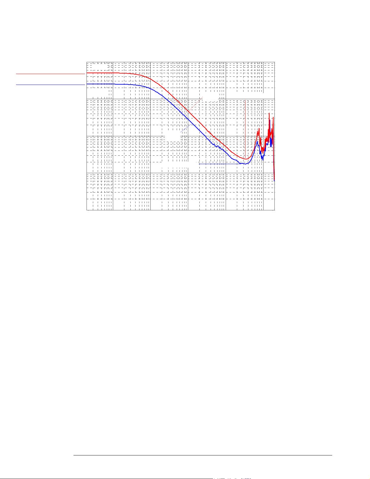
Figure 1-10
Differential Mode Input
Single-ended Mode Input
Differential and Single-ended Probe Configurations
2 Socketed Differential Probe Head (Full Bandwidth)
5
10
50 kΩ
25 kΩ
4
10
3
Ω
10
2
10
0.56 pF
Zmin = 174.6 Ω
0.34 pF
Zmin = 234.9 Ω
1
10
6
10
Magnitude plot of probe input impedance versus frequency.
7
10
8
10
9
10
10
10
Frequency (Hz)
1–24
Page 29

Figure 1-11
Differential and Single-ended Probe Configurations
3 Differential Browser
3 Differential Browser
0.2
Vsource
tr = 98 ps
0.15
0.1
Volts
0.05
0
-0.05
0 0.2 0.4 0.6 0.8 1 1.2 1.4 1.6 1.8 2
Graph of 25 Ω 100 ps step generator with and without probe connected.
Figure 1-12
0.2
Vout
tr = 109 ps
0.15
0.1
Volts
0.05
Vin
tr = 124 ps
Vin
tr = 124 ps
Time (Seconds)
x 10
-9
0
-0.05
0 0.2 0.4 0.6 0.8 1 1.2 1.4 1.6 1.8 2
Graph of Vin and Vout of probe with a 25 Ω 100 ps step generator.
Time (Seconds)
x 10
-9
1–25
Page 30

Figure 1-13
Differential and Single-ended Probe Configurations
3 Differential Browser
6
3
0
dB
-3
Vout
-6
-9
-12
8
10
9
10
Frequency (Hz)
Graph of Vin and Vout of probe with a 25 Ω source and Vout/Vin frequency response.
Figure 1-14
0
-10
Vout/Vin
10
Vin
10
-20
-30
dB
-40
-50
-60
8
10
9
10
Frequency (Hz)
Graph of Vout/Vin frequency response when inputs driven in common (common mode rejection).
10
10
1–26
Page 31

Figure 1-15
Differential Mode Input
Single-ended Mode Input
Differential and Single-ended Probe Configurations
3 Differential Browser
5
10
50 kΩ
25 kΩ
4
10
0.57 pF
3
Ω
10
0.32 pF
Zmin = 229.2 Ω
2
10
1
10
6
10
Magnitude plot of probe input impedance versus frequency.
Zmin = 153.4 Ω
7
10
Frequency (Hz)
10
8
9
10
10
10
1–27
Page 32

Figure 1-16
Differential and Single-ended Probe Configurations
4 Solder-in Single-ended Probe Head (Full Bandwidth)
4 Solder-in Single-ended Probe Head (Full Bandwidth)
0.2
Vsource
tr= 98 ps
0.15
0.1
Vin
tr = 128 ps
Volts
0.05
0
-0.05
0 0.2 0.4 0.6 0.8 1 1.2 1.4 1.6 1.8 2
Graph of 25 Ω 100 ps step generator with and without probe connected.
Figure 1-17
0.2
0.15
0.1
Vout
tr= 118 ps
Vin
tr = 128 ps
Volts
0.05
Time (Seconds)
x 10
-9
0
-0.05
0 0.2 0.4 0.6 0.8 1 1.2 1.4 1.6 1.8 2
Graph of Vin and Vout of probe with a 25 Ω 100 ps step generator.
1–28
Time (Seconds)
x 10
-9
Page 33

Figure 1-18
Differential and Single-ended Probe Configurations
4 Solder-in Single-ended Probe Head (Full Bandwidth)
6
3
0
dB
-3
Vout
-6
-9
-12
8
10
9
10
Frequency (Hz)
Graph of Vin and Vout of probe with a 25 Ω source and Vout/Vin frequency response.
Figure 1-19
0
-10
Vout/Vin
Vin
10
10
-20
-30
dB
-40
-50
-60
8
10
9
10
Frequency (Hz)
Graph of Vout/Vin frequency response when inputs driven in common (common mode rejection).
10
10
1–29
Page 34

Figure 1-20
Differential and Single-ended Probe Configurations
4 Solder-in Single-ended Probe Head (Full Bandwidth)
5
10
25 kΩ
4
10
3
Ω
10
0.50 pF
2
10
1
10
6
10
Magnitude plot of probe input impedance versus frequency.
Zmin = 142.9 Ω
7
10
Frequency (Hz)
10
8
9
10
10
10
1–30
Page 35

Figure 1-21
Differential and Single-ended Probe Configurations
5 Single-ended Browser
5 Single-ended Browser
0.2
Vsource
tr = 98 ps
0.15
0.1
Vin
tr = 135 ps
Volts
0.05
0
-0.05
0 0.2 0.4 0.6 0.8 1 1.2 1.4 1.6 1.8 2
Graph of 25 Ω 100 ps step generator with and without probe connected.
Figure 1-22
0.2
Vout
tr = 125 ps
0.15
Vin
0.1
tr = 135 ps
Volts
0.05
Time (Seconds)
x 10
-9
0
-0.05
0 0.2 0.4 0.6 0.8 1 1.2 1.4 1.6 1.8 2
Graph of Vin and Vout of probe with a 25 Ω 100 ps step generator.
Time (Seconds)
x 10
-9
1–31
Page 36

Figure 1-23
Differential and Single-ended Probe Configurations
5 Single-ended Browser
6
3
0
dB
-3
Vout
-12
-6
-9
8
10
9
10
Frequency (Hz)
Graph of Vin and Vout of probe with a 25 Ω source and Vout/Vin frequency response.
Figure 1-24
0
-10
Vout/Vin
Vin
10
10
-20
-30
dB
-40
-50
-60
8
10
9
10
Frequency (Hz)
Graph of Vout/Vin frequency response when inputs driven in common (common mode rejection).
10
10
1–32
Page 37

Figure 1-25
Differential and Single-ended Probe Configurations
5 Single-ended Browser
5
10
25 kΩ
4
10
3
Ω
10
0.65 pF
2
10
1
10
6
10
Magnitude plot of probe input impedance versus frequency.
Zmin = 120 Ω
7
10
Frequency (Hz)
10
8
9
10
10
10
1–33
Page 38

Figure 1-26
Differential and Single-ended Probe Configurations
6 Solder-in Differential Probe Head (Medium Bandwidth)
6 Solder-in Differential Probe Head (Medium Bandwidth)
0.2
Vsource
tr = 97 ps
0.15
0.1
Vin
tr = 115 ps
Volts
0.05
0
-0.05
0 0.2 0.4 0.6 0.8 1 1.2 1.4 1.6 1.8 2
Graph of 25 Ω 100 ps step generator with and without probe connected.
Figure 1-27
0.2
0.15
0.1
Volts
0.05
Vin
tr = 115 ps
Vin
tr = 192 ps
Time (Seconds)
x 10
-9
0
-0.05
0 0.2 0.4 0.6 0.8 1 1.2 1.4 1.6 1.8 2
Graph of Vin and Vout of probe with a 25 Ω 100 ps step generator.
1–34
Time (Seconds)
x 10
-9
Page 39

Figure 1-28
Differential and Single-ended Probe Configurations
6 Solder-in Differential Probe Head (Medium Bandwidth)
6
3
0
dB
-3
Vout
-12
-6
-9
8
10
9
10
Frequency (Hz)
Graph of Vin and Vout of probe with a 25 Ω source and Vout/Vin frequency response.
Figure 1-29
0
-10
-20
Vout/Vin
Vin
10
10
-30
dB
-40
-50
-60
8
10
9
10
Frequency (Hz)
Graph of Vout/Vin frequency response when inputs driven in common (common mode rejection).
10
10
1–35
Page 40

Figure 1-30
Differential Mode Input
Single-ended Mode Input
Differential and Single-ended Probe Configurations
6 Solder-in Differential Probe Head (Medium Bandwidth)
5
10
50 kΩ
25 kΩ
4
10
0.52 pF
3
Ω
10
Zmin = 251.6 Ω
2
10
0.33 pF
Zmin = 343.3 Ω
1
10
6
10
Magnitude plot of probe input impedance versus frequency.
7
10
8
10
9
10
10
10
Frequency (Hz)
1–36
Page 41

Figure 1-31
Differential and Single-ended Probe Configurations
7 Solder-in Single-ended Probe Head (Medium Bandwidth)
7 Solder-in Single-ended Probe Head (Medium Bandwidth)
0.2
Vsource
tr = 98 ps
0.15
0.1
Vin
tr = 120 ps
Volts
0.05
0
-0.05
0 0.2 0.4 0.6 0.8 1 1.2 1.4 1.6 1.8 2
Graph of 25 Ω 100 ps step generator with and without probe connected.
Figure 1-32
0.2
0.15
0.1
Vin
tr = 120 ps
Vout
tr = 180 ps
Volts
0.05
Time (Seconds)
x 10
-9
0
-0.05
0 0.2 0.4 0.6 0.8 1 1.2 1.4 1.6 1.8 2
Graph of Vin and Vout of probe with a 25 Ω 100 ps step generator.
Time (Seconds)
x 10
-9
1–37
Page 42

Figure 1-33
dB
Differential and Single-ended Probe Configurations
7 Solder-in Single-ended Probe Head (Medium Bandwidth)
6
3
Vout/Vin
0
-3
Vin
Vout
9
10
-12
-6
-9
8
10
Frequency (Hz)
Graph of Vin and Vout of probe with a 25 Ω source and Vout/Vin frequency response.
Figure 1-34
0
-10
-20
-30
dB
-40
10
10
-50
-60
8
10
9
10
Frequency (Hz)
Graph of Vout/Vin frequency response when inputs driven in common (common mode rejection).
1–38
10
10
Page 43

Figure 1-35
Differential and Single-ended Probe Configurations
7 Solder-in Single-ended Probe Head (Medium Bandwidth)
5
10
25 kΩ
4
10
3
Ω
10
2
10
1
10
6
10
Magnitude plot of probe input impedance versus frequency.
0.58 pF
Zmin = 197.6 Ω
7
10
Frequency (Hz)
8
10
9
10
10
10
1–39
Page 44

Figure 1-36
Differential and Single-ended Probe Configurations
8 Socketed Differential Probe Head with Damped Wire Accessory
8 Socketed Differential Probe Head with Damped Wire Accessory
Due to reflections on the long wire accessories, signals being probed should be limited to ~ ≥240
ps rise time measured at the 10 % and 90 % amplitude levels. This is equivalent to ~
bandwidth.
0.2
Vsource
0.15
Volts
0.05
tr = 240 ps
0.1
Vin
tr = 258 ps
≤1.5 GHz
0
-0.05
0 0.2 0.4 0.6 0.8 1 1.2 1.4 1.6 1.8 2
Graph of 25 Ω 240 ps step generator with and without probe connected.
Figure 1-37
0.2
Vin
tr = 258 ps
0.15
0.1
Volts
0.05
0
Vout
tr = 358 ps
Time (Seconds)
x 10
-9
-0.05
0 0.2 0.4 0.6 0.8 1 1.2 1.4 1.6 1.8 2
Graph of Vin and Vout of probe with a 25 Ω 240 ps step generator.
1–40
Time (Seconds)
x 10
-9
Page 45

Figure 1-38
Differential and Single-ended Probe Configurations
8 Socketed Differential Probe Head with Damped Wire Accessory
6
3
0
dB
Vout/Vin
-3
Vout
9
10
-12
-6
-9
8
10
Frequency (Hz)
Graph of Vin and Vout of probe with a 25 Ω source and Vout/Vin frequency response.
Figure 1-39
0
-10
-20
Vin
10
10
-30
dB
-40
-50
-60
8
10
9
10
Frequency (Hz)
Graph of Vout/Vin frequency response when inputs driven in common (common mode rejection).
10
10
1–41
Page 46

Figure 1-40
Differential Mode Input
Differential and Single-ended Probe Configurations
8 Socketed Differential Probe Head with Damped Wire Accessory
5
10
50 kΩ
Single-ended Mode Input
25 kΩ
4
10
3
Ω
10
Zmin = 248.9 Ω
2
10
1
10
6
10
Magnitude plot of probe input impedance versus frequency.
0.95 pF
7
10
0.63 pF
10
Frequency (Hz)
8
Zmin = 344.0 Ω
9
10
10
10
1–42
Page 47

2
Service
Page 48

Service
The service section of this manual contains the following information:
• Service Strategy for the 1134A probe
• Cleaning the 1134A probe
• Returning the 1134A probe to Agilent Technologies for service
• Recommended tools and test equipment
• Calibration Testing Procedures
• To Test Bandwidth
• Performance test record
• Replaceable parts and accessories
2–2
Page 49

Table 2-1
Service
Service Strategy for the 1134A Probe
Service Strategy for the 1134A Probe
This chapter provides service information for the 1134A family of Active and Differential Probes.
The following sections are included in this chapter.
• Service strategy
• Returning to Agilent Technologies for service
•Troubleshooting
• Failure symptoms
The 1134A Active Probe is a high frequency device with many critical relationships between
parts. For example, the frequency response of the amplifier on the hybrid is trimmed to match
the output coaxial cable. As a result, to return the probe to optimum performance requires
factory repair. If the probe is under warranty, normal warranty services apply.
There is one warranted specification which is listed below.
Description Specification Further Information
Bandwidth 7 GHz
You may perform the tests in the "Calibration and Operational Verification Tests" later in this
chapter to ensure these specifications are met.
If the probe is found to be defective we recommend sending it to an authorized service center
for all repair and calibration needs. Please see the "Returning to Agilent Technologies for Service"
section later in this chapter.
2–3
Page 50

Service
To return the probe to Agilent Technologies for service
To return the probe to Agilent Technologies for service
Follow the following steps before shipping the 1134A back to Agilent Technologies for service.
1
Contact your nearest Agilent sales office for information on obtaining an RMA number
and return address.
2 Write the following information on a tag and attach it to the malfunctioning equipment.
Name and address of owner
Product model number Example 1134A
Product Serial Number Example MYXXXXXXXX
Description of failure or service required
Include probing and browsing tips if you feel the probe is not meeting performance specifications or a
yearly calibration is requested.
Protect the 1134A Probe by wrapping in plastic or heavy paper.
3
4 Pack the 1134A Probe in the original carrying case or if not available use bubble wrap
or packing peanuts.
5 Place securely in sealed shipping container and mark container as "FRAGILE".
If any correspondence is required, refer to the product by serial number and model number.
2–4
Page 51

Service
Troubleshooting
Troubleshooting
• If your probe is under warranty and requires repair, return it to Agilent Technologies. Contact
your nearest Agilent Technologies Service Center.
• If the failed probe is not under warranty, you may exchange it for a reconditioned probe. See
"To Prepare the Probe for Exchange" in this chapter.
2–5
Page 52

Service
Failure Symptoms
Failure Symptoms
The following symptoms may indicate a problem with the probe or the way it is used. Possible
remedies and repair strategies are included.
The most important troubleshooting technique is to try different combinations of equipment so
you can isolate the problem to a specific probe.
Probe Calibration Fails
Probe calibration failure with an oscilloscope is usually caused by improper setup. If the
calibration will not pass, check the following:
• Check that the probe passes a waveform with the correct amplitude.
• If the probe is powered by the oscilloscope, check that the offset is approximately correct. The
probe calibration cannot correct major failures.
• Be sure the oscilloscope passes calibration without the probe.
Incorrect Pulse Response (flatness)
If the probe's pulse response shows a top that is not flat, check for the following:
• Output of probe must be terminated into a proper 50 Ω termination. If you are using the probe
with an Infiniium oscilloscope, this should not be a problem. If you are using the probe with
other test gear, insure the probe is terminated into a low reflectivity 50 Ω load (~ ± 2%).
• If the coax or coaxes of the probe head in use has excessive damage, then reflections may be
seen within ~ 1 ns of the input edge. If you suspect a probe head, swap it with another probe
head and see if the non-flatness problem is fixed.
• If the one of the components in the tip have been damaged there may be a frequency gain nonflatness at around 40 MHz. If you suspect a probe head, swap it with another probe head and
see if the non-flatness problem is fixed.
Incorrect Input Resistance
The input resistance is determined by the probe head in use. If the probe head is defective,
damaged, or has been exposed to excessive voltage, the input resistor may be damaged. If this
is the case, the probe head is no longer useful. A new probe head will need to be obtained either
through purchase or warranty return.
Incorrect Offset
Assuming the probe head in use is properly functioning, incorrect offset may be caused by defect
or damage to the probe amplifier or by lack of probe calibration with the oscilloscope.
2–6
Page 53

Calibration Testing Procedures
Calibration Testing Procedures
These tests can be performed to ensure the 1134A Probe meets specifications.
Some tests require the probe to be calibrated on an Infiniium oscilloscope channel before testing
performance.
Service
2–7
Page 54

Table 2-2
Service
To Test Bandwidth
To Test Bandwidth
This test ensures that the 1134A Probe meets its specified bandwidth.
1134A >7 GHz
Equipment/Tool Critical Specification Model Number
Vector Network Analyzer (VNA) 7 GHz sweep range full 2 port cal Option 1D5 Agilent 8720ES
Calibration Standards No Substitute Agilent 85052D
External Power Supply No Substitute Agilent 1143A
AutoProbe Interface Adapter No Substitute Agilent N1022A
Outside thread 3.5 mm (male) to
3.5 mm (female) adapter
Cable (2) 3.5 mil; SMA; High Quality Agilent 8120-4948
Cable 1.5 mil Probe Power Extension No Substitute Agilent 01143-61602
PV/DS Test Board No Substitute (In E2655A Kit) Agilent E2655-66501
No Substitute Agilent 5062-1247
Using the 8720ES VNA successfully
Remember these simple guidelines when working with the 8720ES VAN to get accurate stable
measurements.
1 Sometimes it may take a few seconds for the waveforms to settle completely. Please allow time for
waveforms to settle before continuing.
2 Make sure all connections are tight and secure. If needed, use a vice to hold the cables and test board
stable while making measurements.
3 Be careful not to cross thread or force any connectors. This could be a very costly error to correct.
Initial Setup
1
Turn on the 8720ES VNA and let warm up for 20 minutes.
2 Press the green "Preset" key on the 8720ES VNA.
3 Use the 8720ES VNA's default power setting of 0 dBm. You can locate this feature by
pressing the "Power" key on the front panel.
4 Set the 8720ES VNA's averaging to 4. You can find this selection menu by pressing the
"AVG" key. Then select the "Averaging Factor" screen key to adjust the averaging.
5 Press the "Sweep Setup" key on the 8720ES VNA. Then press the "sweep type menu"
screen key. Select the "log freq" screen key.
6 Connect the 1134A probe under test to the Auto Probe Adapter and power the probe
using the 1143A power supply. Install the outside thread adapter to the Auto Probe
Adapter.
2–8
Page 55

Figure 2-1
Service
To Test Bandwidth
Calibrating a Reference Plane
To get a reliable measurement from the 8720ES VNA we must calibrate a reference plane so that the
8720ES VNA knows where the probe under test is located along the transmission line.
2–9
Page 56

Service
To Test Bandwidth
Press the "Cal" key on the 8720ES VNA.
1
8120-4948
E2655-66501
Reference
Plane
2 Then Press the "cal menu" screen key.
3 Finally, press the "full 2 port" screen key.
4 Connect one of the high quality SMA cables to port one and to the pincher side of PV/
DS test board.
5 The calibration reference plane is at the other end of PV/DS test board.
2–10
Page 57

Figure 2-2
Service
To Test Bandwidth
8120-4948
E2655-66501
Perform Calibration for the port one side of the Reference plane.
6
• Press the "reflection" screen key
• Connect open end of 85052D to the non-pincher side of the PV/DS test board.
• Select the "open" screen key under the "Forward" group.
• The 8720ES VAN will beep when done.
• Connect short end of 85052D to the non-pincher side of the PV/DS test board.
• Select "short" screen key under the "Forward" group.
• The 8720ES VAN will beep when done.
• Connect load end of 85052D to the non-pincher side of the PV/DS test board.
• Select the "loads" screen key under the "Forward" group.
• Press "broadband" screen key selection.
• The 8720ES VAN will beep when done.
• Press the "done loads" screen key.
• You have just calibrated one side of the reference plane.
Connect the other high quality SMA cable to port two of the 8720ES VNA.
7
Reference
Plane
2–11
Page 58

Figure 2-3
Service
To Test Bandwidth
8120-4948
Reference
Plane
Get the opposite sex of the 85052D calibration standards for the next step.
8
9 Perform Calibration for the port two side of the Reference plane.
• Press the "reflection" screen key.
• Connect open end of 85052D to the available end of the port two SMA cable.
• Selec8720ES t the "open" screen key under the "Reverse" group.
• The 8720ES VNA will beep when done.
• Connect short end of 85052D to the available end of the port two SMA cable.
• Select "short" screen key the "Reverse" group.
• The 8720ES VNA will beep when done.
• Connect load end of 85052D to the available end of the port two SMA cable.
• Select the "loads" screen key the "Reverse" group.
• Press "broadband" screen key selection.
• The 8720ES VNA will beep when done.
• Press the "done loads" screen key.
• You have just calibrated the other side of the reference plane.
Press "standards done" key.
10
11 Connect port two SMA cable to the non-pincher side of PV/DS test board.
2–12
Page 59

Figure 2-4
Service
To Test Bandwidth
8120-4948
Press the "transmission" screen key.
12
8120-4948
E2655-66501
Reference
Plane
13 Press the "do both fwd and reverse" screen key.
14 The 8720ES VNA will beep four times when done.
15 Press the "isolation" screen key.
16 Press the "omit isolation" screen key.
17 Press "done 2 port cal" screen key.
18 Set the 8720ES VNA's averaging to off.
19 Save the reference plane cal by pressing the "save recall" key then the "save state" key.
20 You may change name if you wish.
21 Press the "scale reference" key. Then
Set for 1 dB per division.
Set reference position for 7 divisions.
Set reference value for 0 dB
22
Press the "measure" key.
23 Press the "s21" screen key.
24 Ensure s21 response on screen is flat (about ± 0.1 dB) out to 10 GHz.
2–13
Page 60

Figure 2-5
Service
To Test Bandwidth
Measuring Vin Response
Position 1134A probe conveniently to make quality connections on the PV/DS board.
1
2 Ensure resistors at the probe tip are reasonably straight and about 0.1 inches apart.
3 Connect probe tip under pincher on PV/DS board
Apply upward pressure to the clip to insure proper electrical connection.
Place the "+" side on center conductor and "-" side to ground.
Press the "Sweep Setup" key on the 8720ES VNA. Then press the "trigger menu" screen
key. Select the "continuous" screen key.
4
You should now have the Vin waveform on screen. It should look similar to Figure 2-5.
5
Select "display key" then "data->memory" screen key.
6 You have now saved Vin waveform into the 8720ES VNA's memory for future use.
2–14
Page 61

Figure 2-6
To Test Bandwidth
Measuring Vout Response
Disconnect the port 2 cable from PV/DS test board and attach to probe output on the
1
AutoProbe Adapter.
2 Connect the 85052D cal standard load to PV/DS test board (non-pincher side).
3 Press "scale reference" key on the 8720ES VNA.
4 Set reference value to -20 dB.
5 The display on screen is Vout. It should look similar to Figure 2-6.
Service
Displaying Vin/Vout Response on 8720ES VNA Screen
1
Press the "Display" Key.
2 Then select the "Data/Memory" Screen Key. The display should look similar to
Figure 2-7.
3 Press marker key and position the marker to the first point that the signal is below -3 dB.
4 Read marker frequency measurement and record it in the test record located later in
this chapter.
5 The bandwidth test passes if the frequency measurement is greater that the probe's
bandwidth limit. Example: > 7 GHz.
2–15
Page 62

Figure 2-7
Service
To Test Bandwidth
2–16
Page 63

Performance Test Record
Test Name Results
Bandwidth >7 GHz
Service
Performance Test Record
Result _______ GHz
Pass/Fail
2–17
Page 64

Service
Replaceable Parts and Accessories
Replaceable Parts and Accessories
See the "User’s Quick Start Guide" for a list of replaceable parts and
accessories.
2–18
Page 65

B
bandwidth test 2-8
C
calibration
failure 2-6
calibration procedure 2-7
cleaning the instrument 3
F
failure symptoms 2-6
I
instrument, cleaning the 3
P
packing for return 2-4
parts
replaceable 2-18
Index
R
repair 2-4
replacement parts 2-18
returning probe to Agilent Technologies 2-4
S
service
strategy 2-3
specifications
warrantied 2-3
T
test
bandwidth 2-8
troubleshooting 2-5
Index-1
Page 66

Index-2
Page 67

Safety
Notices
This apparatus has been
designed and tested in accordance with IEC Publication 1010,
Safety Requirements for Measuring Apparatus, and has been
supplied in a safe condition.
This is a Safety Class I instrument (provided with terminal for
protective earthing). Before
applying power, verify that the
correct safety precautions are
taken (see the following warnings). In addition, note the
external markings on the instrument that are described under
"Safety Symbols."
Warnings
• Before turning on the instrument, you must connect the protective earth terminal of the
instrument to the protective conductor of the (mains) power
cord. The mains plug shall only
be inserted in a socket outlet
provided with a protective earth
contact. You must not negate
the protective action by using an
extension cord (power cable)
without a protective conductor
(grounding). Grounding one
conductor of a two-conductor
outlet is not sufficient protection.
• Only fuses with the required
rated current, voltage, and specified type (normal blow, time
delay, etc.) should be used. Do
not use repaired fuses or shortcircuited fuseholders. To do so
could cause a shock or fire hazard.
• If you energize this instrument
by an auto transformer (for voltage reduction or mains isolation), the common terminal must
be connected to the earth terminal of the power source.
• Whenever it is likely that the
ground protection is impaired,
you must make the instrument
inoperative and secure it against
any unintended operation.
• Service instructions are for
trained service personnel. To
avoid dangerous electric shock,
do not perform any service
unless qualified to do so. Do not
attempt internal service or
adjustment unless another person, capable of rendering first
aid and resuscitation, is present.
• Do not install substitute parts
or perform any unauthorized
modification to the instrument.
• Capacitors inside the instrument may retain a charge even if
the instrument is disconnected
from its source of supply.
• Do not operate the instrument
in the presence of flammable
gasses or fumes. Operation of
any electrical instrument in such
an environment constitutes a
definite safety hazard.
• Do not use the instrument in a
manner not specified by the
manufacturer.
To clean the instrument
If the instrument requires cleaning: (1) Remove power from the
instrument. (2) Clean the external surfaces of the instrument
with a soft cloth dampened with
a mixture of mild detergent and
water. (3) Make sure that the
instrument is completely dry
before reconnecting it to a
power source.
Safety Symbols
!
Instruction manual symbol: the
product is marked with this symbol when it is necessary for you
to refer to the instruction manual in order to protect against
damage to the product..
Hazardous voltage symbol.
Earth terminal symbol: Used to
indicate a circuit common connected to grounded chassis.
Agilent Technologies Inc.
P.O. Box 2197
1900 Garden of the Gods Road
Colorado Springs, CO 80901-2197, U.S.A.
Page 68

Notices
© Agilent Technologies, Inc. 20022004
No part of this manual may be
reproduced in any form or by any
means (including electronic
storage and retrieval or
translation into a foreign
language) without prior
agreement and written consent
from Agilent Technologies, Inc. as
governed by United States and
international copyright laws.
Manual Part Number
01134-97009, May 2004
Print History
01134-97001, November 2002
01134-97003, January 2003
01134-97004, June 2003
01134-97007, September 2003
01134-97009, May 2004
Agilent Technologies, Inc.
1900 Garden of the Gods Road
Colorado Springs, CO 80907 USA
Restricted Rights Legend
If software is for use in the performance of a U.S. Government
prime contract or subcontract,
Software is delivered and
licensed as “Commercial computer software” as defined in
DFAR 252.227-7014 (June 1995),
or as a “commercial item” as
defined in FAR 2.101(a) or as
“Restricted computer software”
as defined in FAR 52.227-19
(June 1987) or any equivalent
agency regulation or contract
clause. Use, duplication or disclosure of Software is subject to
Agilent Technologies’ standard
commercial license terms, and
non-DOD Departments and
Agencies of the U.S. Government will receive no greater
than Restricted Rights as
defined in FAR 52.227-19(c)(1-2)
(June 1987). U.S. Government
users will receive no greater
than Limited Rights as defined in
FAR 52.227-14 (June 1987) or
DFAR 252.227-7015 (b)(2)
(November 1995), as applicable
in any technical data.
Document Warranty
The material contained in
this document is provided
“as is,” and is subject to
being changed, without
notice, in future editions.
Further, to the maximum
extent permitted by applicable law, Agilent disclaims
all warranties, either
express or implied, with
regard to this manual and
any information contained
herein, including but not
limited to the implied warranties of merchantability
and fitness for a particular
purpose. Agilent shall not be
liable for errors or for incidental or consequential
damages in connection with
the furnishing, use, or performance of this document
or of any information contained herein. Should Agilent and the user have a
separate written agreement
with warranty terms covering the material in this document that conflict with these
terms, the warranty terms in
the separate agreement
shall control.
Technology Licenses
The hardware and/or software
described in this document are
furnished under a license and
may be used or copied only in
accordance with the terms of
such license.
WARNING
A WARNING notice
denotes a hazard. It calls
attention to an operating
procedure, practice, or
the like that, if not
correctly performed or
adhered to, could result
in personal injury or
death. Do not proceed
beyond a WARNING
notice until the indicated
conditions are fully
understood and met.
CAUTION
A CAUTION notice
denotes a hazard. It calls
attention to an operating
procedure, practice, or
the like that, if not
correctly performed or
adhered to, could result in
damage to the product or
loss of important data. Do
not proceed beyond a
CAUTION notice until the
indicated conditions are
fully understood and met.
 Loading...