

AGERE R485JPAA, R485JPBB, R485WMAA, R485WPAA, R485WPBB Datasheet
...
R485-Type Lightwave Receiver with Clock
Recovery for 2.488 Gbits/s Applications
■
Agere Systems Inc. Reliability and Qualification
Program for built-in quality
■
SONET/SDH compatible for OC-48/STM-16 data
rate
Applications
■
Telecommunications
— Inter- and intraoffice SONET/SDH
— Subscribe r loo p
— Metropolitan area networks
Advance Data Sheet, Rev. 1
October 2001
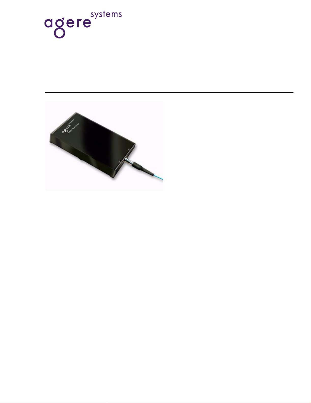
Manufactured in a low-profile, 24-pin package, the R485-Type
Receiver features either an aval anche or PIN photodetector, a
transimpedance amplifier , a limiting ampli fier, and a clock and
data recovery IC.
Features
■
Multisourced footprint
■
Internal APD bias supply
■
Differential data and clock outputs
■
APD and PIN versions
■
Typical sensitivity:
—APD, –32 dBm
—PIN, –23 dBm
■
Operation at 1.3 µm or 1.55 µm
■
TTL link status flag
■
Wide operating case temperature range:
—APD, 0 °C to +70 °C
—PIN, –40 °C to +85 °C
■
Space-saving, self-contained, 24-pin DIP
■
High-speed data communications
Description
The R485-Type 2.5 Gbits/s lightwave receiver is
designed for use in SONET OC-48 and synchronous
digital hierarchy (SDH) STM-16 telecommunications
applications and high-speed data communications
applications. The receiver converts received optical
signals in the range of 1.2 µm to 1.6 µm wavelength
into differential data and clock outputs. The receiver
consists of either InGaAs APD or PIN photodetector
(depending on model selected), a transimpedance
amplifier, a limiting amplifier, and a clock and data
recovery IC (CDR). The CDR uses PLL technology to
extract the clock signal from the converted optical
signal. A TTL compatible link status flag signal indicates when there is a loss of optical signal.
The receiver is manufactured in a low-profile, pigtailed, 24-pin plastic DIP package. It requires a single, +5.0 V power supply. The APD version has the
added benefit of containing the high-voltage supply
internal to the receiver. This internal supply also provides the necessary temperature compensation for
the APD.

R485-Type Lightwave Receiver with Clock
Recovery fo r 2.48 8 Gbits/s Appl ica ti ons
Advance Data Sheet, Rev. 1
October 2001
Flag Output
When the incoming optical signal falls below the linkstatus switching threshold, the FLAG output is asserted
and the FLAG output logic level changes from a TTL
low to a TTL high.
Pin Information
Table 1. Pin Information
Pin Name Pin Name
1 NIC 24 NUC*
2 NUC* 23 NUC*
3LOS Flag
†
22 V
CC
4 Ground 21 NUC*
5CLOCK
20 Ground
6 CLOCK 19 Ground
7 Ground 18 NIC
8V
CC
17 Ground
9 Ground 16 Ground
10 DATA 15 Ground
11 DATA
12 Ground 13 DTV/NIC
* Pins designated as no user connect (NUC) are connected inter-
nally. The user should not make any connections to these pins.
† The loss of signal (LOS) FLAG output is a logic level that indicates
the presence or absence of a minimum acceptable level of optical
input. A TTL logic HIGH indicates the absence of a valid optical
input signal.
‡ This pin is not internally connected if the amplitude decision
threshold (DTV) is not made adjustable.
14 Ground
‡
Handling Precautions
The R485-Type receiver is manufactured with a
39 in. ± 4 in. (100 cm ± 10 cm) single-mode fiber pigtail
with a 900 µm OD PVC outer jacket. Both SC and FC-
PC connectors are offered on standard versions. Other
optical connector options are available on special
order. Please contact an Agere Systems Account Manager for availability and ordering information.
Receiver Processing
The R485-Type receiver devices can withstand normal
wave soldering processes. The complete receiver module is not hermetically sealed; therefore, it should not
be immersed in, or sprayed with, any solutions. The
optical connector process cap deformation temperature
is 85 °C. The receiver pins can be wave soldered at
250 °C for 10 seconds.
Electrostatic Discharge
CAUTION: This device is susceptible to damage as
a result of electrostatic discharge (ESD).
Take proper precautions during both
handling and testing. Follow guidelines
such as JEDEC Publication No. 108-A
(Dec. 1988).
Although protection circuitry is designed into the
device, take proper precautions to avoid exposure to
ESD .
Agere employs a human-body model HBM) for ESDsusceptibility testing and protection design evaluation.
ESD voltage thresholds are dependent on the critical
parameters used to define the model. A standard HBM
(resistance = 1.5 kΩ, capacitance = 100 pF) is widely
used and, therefore, can be used for comparison purposes.
Installation Considerations
Although the receiver has been designed with ruggedness in mind, care should be used during handling.
The optical connector should be kept free from dust.
The optical connector process cap should be kept in
place as a dust cover when the device is not connected
to a cable. If contamination is present on the optical
connector, the use of canned air with a extension tube
should remove any loose debris. Other cleaning procedures are outlined in the
blies
Technical Note (TN95-010LWP).
The cable should be handled conservatively with no
excessive axial pulling or lateral tugging.
Cleaning Fiber Optic Assem-
The minimum fiber bending radius is 1.5 inches
(38 mm).
2 Agere Systems Inc.
Advance Data Sheet, Rev. 1
October 2001
R485-Type Lightwave Receiver with Clock
Recovery for 2.488 Gbits/s Applications
Absolute Maximum Ratings
Stresses in excess of the absolute maximum ratings can cause permanent damage to the device. These are absolute stress ratings only. Functional operation of the device is not implied at these or any other conditions in excess
of those given in the operational sections of the data sheet. Exposure to absolute maximum ratings for extended
periods can adversely affect device reliability.
Parameter Symbol Min Max Unit
Operating Case Temperature Range:
APD
PIN
Storage Temperature T
C
T
C
T
stg
0
–40
70
85
–40 85 °C
Optical Input Power—Biased:
APD
PIN
Supply Voltages V
IN
P
IN
P
CC
—
—
0
8
06.5V
Lead Soldering Temperature/Time — — 250/10 °C/s
°C
°C
dBm
dBm
Characteristics
Table 2. Optical Characteristics
–10
At 1.3 µm wavelength and 1 x 10
Parameter Symbol Min
Measured Average Sensitivity:
APD
PIN
Maximum Input Power:
APD
PIN
Link Status Switching Threshold
Decreasing Light Input:
APD
PIN
Flag Response Time t
Flag Hysteresis — 1.2 — — dB
Optical Reflectance:
Single-mode Fiber
Multimode Fiber
* Over operating temperature range and at end of life.
†Typical values at room temperature and beginning of life.
BER with 223 – 1 NRZ pseudorandom data.
Typ
–32
–23
—
—
–40
–27
MIN
P
MIN
P
MAX
P
MAX
P
LSTD
LSTD
FLAG
*
—
—
–8
0
–45
–34
3 — 1000 µs
—
—
—
—
—
†
Max
*
–30
–21
—
—
–35
–24
–27
–14
Unit
dBm
dBm
dBm
dBm
dBm
dBm
dB
dB
Agere Systems Inc. 3
 Loading...