

AGERE R2560A023 Datasheet
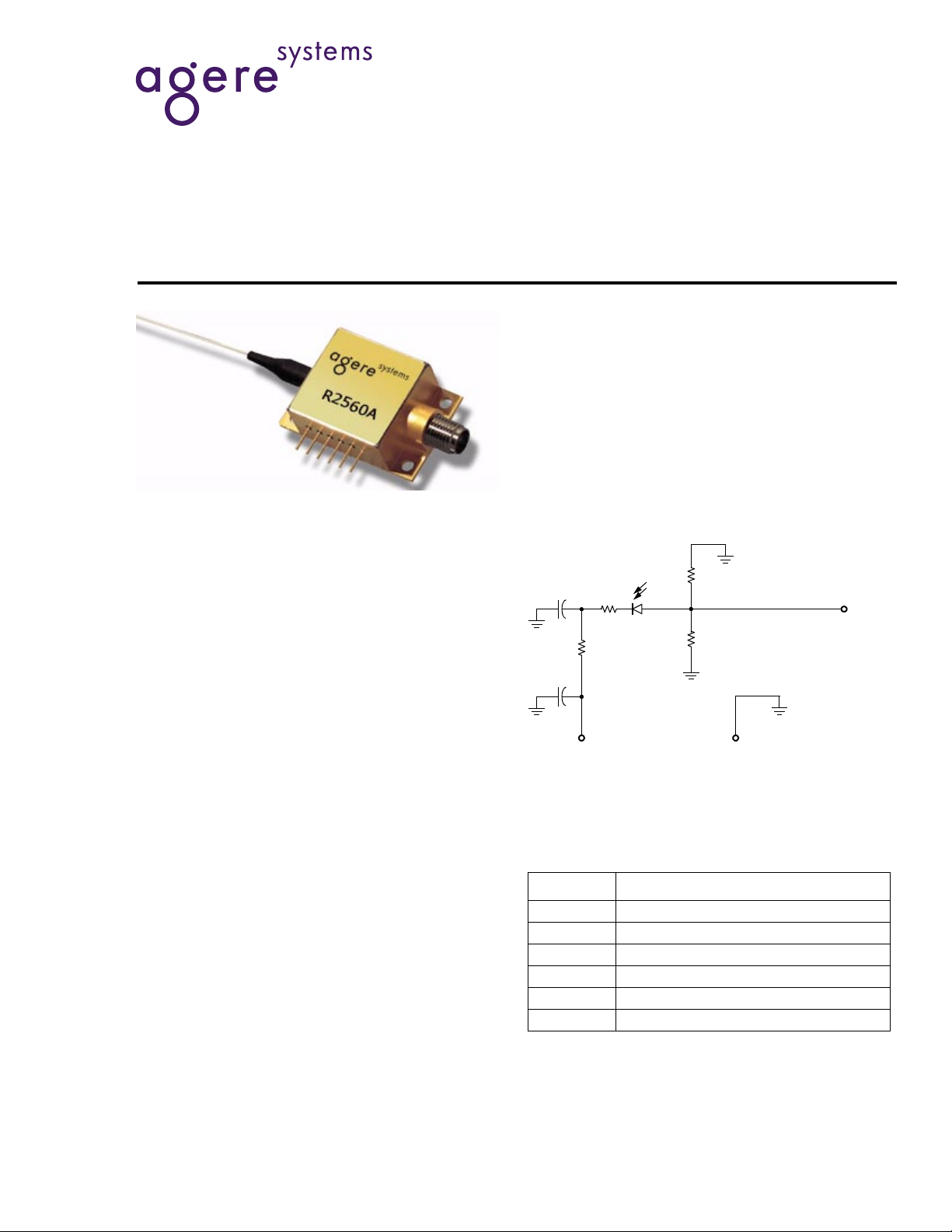
R2560A High-Power 12 GHz Photodiode
100
100
PIN
PHOTODIODE
PIN 3
+10 V BIAS
PIN 6
CASE GROUND
RF OUT
Description
The R2560A incorporates a high-speed planar PIN
diode to provide a highly reliable, high-power photodiode module. This module is well suited for receiver
applications with optical preamplification. The diode
is well matched over the operating frequency band,
thereby simplifying high-speed integration.
Block Diagram
Preliminary Data Sheet, Rev. 1
June 2001
Features
■
Highly reliable planar photodiode technology
■
High power capability
■
dc coupled
■
High breakdown v oltage
■
Bandwidth >13 GHz typical
■
Good RF match: >13 dB typical return loss
■
Hermetically sealed
Applications
■
Optically amplified systems (following EDFA or
Raman amplifiers)
■
Linear receiver applications
■
FEC and Super-FEC to 12.5 Gbits/s
Pin Information
Table 1. Pin Descriptions
Pin No. Description
1NC
2NC
3 10 V (V
4NC
5NC
6 Ground
PD
)
1-1176 (F)
Preliminary Data Sheet, Rev. 1
R2560A High-Power 12 GHz Photodiode June 2001
Absolute Maximum Ratings
Stresses in excess of the absolute maximum ratings can cause permanent damage to the device. These are absolute stress ratings only. Functional operation of the device is not implied at these or any other conditions in excess
of those given in the operational sections of the data sheet. Exposure to absolute maximum ratings for extended
periods can adversely affect device reliability.
Parameter Symbol Min Max Unit
Operating Temperature Range T
OP
070°C
Storage Case Temperature Range Tstg –40 85 °C
Photodiode Bias Voltage V
Av erage Optical Input Power P
PD
IN
—15V
Ò12dBm
Characteristics
Table 2. Electrical/Optical Characteristics
(at 25 °C Case Temperature)
Parameter Symbol Min Typ Max Unit
Optical Wavelength Range λ 1280 — 1580 nm
Gain into a 50 Ω Load for a Given Input
G 17.5 — — V/W
Optical Power Level
Responsivity R 0.7 0.8 — A/W
Dark Current I
Breakdown Voltage (I
High Frequency Cutoff
= 10 µA) V
R
F
D
BR
HIGH
—— 1nA
25 — — V
12 13 — GHz
–3 dB relative to 100MHz
Low Frequency Cutoff F
Group Delay Variation (0.5 GHz—
LOW
—–10— 20 ps
—— 0kHz
13 GHz) Relative to 2 GHz
RF Output Return Loss
RL
RF
10 13 — dB
(0.1 GHz—13 GHz)
Optical Return Loss RL 35 — — dB
Photodiode Supply Voltage (V
)VPD81012V
PD
2
Agere Systems I nc.
 Loading...