

AGERE ORT8850H-3BM680, ORT8850L-3BM680, ORT8850L-2BM680, ORT8850L-2BA352, ORT8850L-1BM680 Datasheet
...
Data Sheet
August 2001
ORCA
®
ORT8850 Field-Programmable System Chip (FPSC)
Eight-Channel x 850 Mbits/s Backplane Transceiver
Introduction
Field-programmab le s y stem c hips (FPSCs) bring a
whole new dimension t o programmable logic: FPG A
logic and an embedded system solution on a single
device. Agere Systems Inc. has developed a solution
for designers who need the many advantages of
FPGA-based design im plementation, coupled wit h
high-speed serial backplane data transfer. Built on the
Series 4 reconfigurable embedded system-on-chips
(SoC) architecture, the ORT8850 family is made up of
backplane transceivers containing eight channels,
each operating at up to 850 Mbits/s (6.8 Gbits/s when
all eight channels are use d) f ull-duplex synchronous
interface, with built-in clock and data recovery (CDR)
in standard-cell logic, along with up to 600K usable
FPGA system gates. The CDR cir cu i tr y i s a macrocell
available from Agere’s Smart S ilic on macro library,
and has already been implemented in numerous
applications including ASICs, standard products, and
FPSCs to create interfaces for SONET/SDH STS-3/
STM-1, STS-12/STM-4, STS-48/STM-16, a nd ST S192/STM-64 applications. With the addition of protocol
and access logic such a s pr ot oc ol-independent framers, asynchronous trans f er mode (ATM) framers,
packet-over-SONET (POS) interfaces, and framers for
HDLC for Inte rnet protoc ol (IP), desi gners can build a
configurable interface retaining proven backplane
driver/receiver technology. Designers can also use the
device to drive high-speed data transfer across buses
within a system that are not SONET/SDH based. For
example, designers can build a 6.8 Gbits/s PCI-to-PCI
half bridge using our PCI soft core.
The ORT8850 family offers a clockless high-speed
interface for interdevice communication, on a board or
across a backplane. The built-in clock recovery of the
ORT8850 allows for higher system performance, easier-to-design clock domains in a multiboard system,
and fewer signals on the bac k plane. Network design ers will benefit from the ba c kp lane transceiver as a
network termination de vice. The backplane trans ceiver of fe rs S ONET s cra mblin g/de scr ambl ing o f da ta
and streamlined SONET framing, pointer moving, and
transport overhead ha ndling, plus the programmable
logic to terminate the network into proprietary systems. For non-SONET application, all SONET functionality is hidden from the user and no prior
networking knowledge is required. The 8850 also
offers 8B/10B coding in addition to SONET scrambling.
Also included on the device are three full-duplex, highspeed parallel interface s, c ons is t ing of 8-bit data, control (such as start-of-cell), and clock. The interface
delivers double data rate (DDR) data at rates up to
311 MHz (622 Mbits/s per pin), and converts this data
internal t o the device in t o 32-bit wide data running at
half rate on one clock edge. Functions such as centering the transmit clock in th e t rans m it data eye are
done automatically by the interface. Applications
delivered by this interface include a parallel backplane
interface similar to the rec ent ly proposed
RapidIO
™
packet-based interface.
Table 1.
ORCA
®
ORT8850 Family—Available FPGA Logic
Note: The embedded core and interface are not included in the above gate counts.The usable gate counts range from a logic-only gate
count to a gate count assuming 20% of the PFUs/SLICs being used as RAMs. The logic-only gate count includes each PFU/SLIC
(counted as 108 gates/PFU), including 12 gates per LUT/FF pair (eight per PFU), and 12 gates per SLIC/FF pair (one per PFU).
Each of the four PIO groups are counted as 16 gates (three FFs, fast-capture latch, output logic, CLK, and I/O buffers). PFUs used
as RAM are counted at four gates per bit, with each PFU capable of implementing a 32 x 4 RAM (or 512 gates) per PFU. Embedded
block RAM (EBR) is counted as four gates per bit plus each block has an additional 25K gates. 7K gates are used for each PLL and
50K gates for the embedded system bus and microprocessor interface logic. Both the EBR and PLLs are conservatively utilized in
the gate calculations.
Device PFU Rows
PFU
Columns
Total
PFUs
FPGA
User I/O
LUTs
EBR
Blocks
EBR Bits
(K)
Usable
Gates (K)
ORT8850L 26 24 624 296 4,992 8 74 260—470
ORT8850H 46 44 2024 536 16,192 16 147 530—970

Table of Contents
Contents Page Contents Page
2 Agere Systems Inc.
Data Sheet
August 2001
Eight-Channel x 850 Mbits/s Backplane Transceiver
ORCA
ORT8850 FPSC
Introduction..................................................................1
Embedded Core Features (Serial)...............................4
Embedded Core Features (Parallel)............................4
Programmable FPGA Features...................................5
Programmable Logic System Features .......................6
Description...................................................................7
What Is an FPSC? ...................................................7
FPSC Overview .......................................................7
FPSC Gate Counting ...............................................7
FPGA/Embedded Core Interface .............................7
ORCA
Foundry Development System .....................7
FPSC Design Kit ......................................................8
FPGA Logic Overview ..............................................8
PLC Logic ................................................................8
Programmable I/O ....................................................9
Routing ...................... ................... ................... .........9
System-Level Features..............................................10
Microprocessor Interface .......................................10
System Bus ............................................................10
Phase-Locked Loops ...................................... .......10
Embedded Block RAM ...........................................10
Configuration ................... .......................... .............11
Additional Information ............................................11
ORT8850 Overview...................................................12
Device Layout ........................................................12
Backplane Transceiver Interface ...........................12
HSI Interface ..........................................................15
STM Macrocell .......................................................15
8B/10B Encoder/Decoder ......................................15
FPGA Interface ......................................................15
Byte-Wide Parallel Interface ..................................15
FPSC Configuration ...............................................16
Generic Backplane Transc eiv er Appli cation..............17
Synchronous Transfer Mode (STM) .......................17
8B/10B Mode .........................................................17
Backplane Transceiver Core Detailed Description....18
HSI Macro ..............................................................18
STM Transmitter (FPGA Æ Backplane) .................20
STM Receiver ( Backplane Æ FPGA) .....................23
8B/10B Transmitter (FPGA Æ Backplane) ............30
8B/10B Receiver (Backplane Æ FPGA) ................30
Pointer Mover Block (Backplane Æ FPGA) ...........31
Receive Bypass Options and FPGA Interface .......33
Powerdown Mode ................................................. 33
STM Redundancy and Protection Switching ......... 33
LVDS Protection Switching ................................... 34
RapidIO
Interface to Pi-Sched.................................. 34
Overview ............................................................... 34
Receive Cell Interface ........................................... 34
Transmit Cell Interface .......................................... 36
Memory Map............................................................. 38
Definition of Register Types .................................. 38
Absolute Maximum Ratings...................................... 55
Recommended Operating Conditions ...................... 55
Power Supply Decoupling LC Circuit........................ 56
HSI Electrical and Timing Characteristics ................ 57
Parallel
RapidIO
-like Interface Timing
Characteristics......................................................... 58
Embedded Core LVDS I/O ....................................... 59
LVDS Receiver Buffer Requirements .................... 60
Input/Output Buffer Measurement Conditions
(on-LVDS Buffer)..................................................... 61
LVDS Buffer Characteristics..................................... 62
Termination Resistor ............................................. 62
LVDS Driver Buffer Capabilities ............................ 62
Pin Information ......................................................... 63
Package Pinouts ................................................... 77
Package Thermal Characteristics Summary .......... 105
Θ
JA ..................................................................... 105
Ψ
JC ............................. ........................................ 105
Θ
JC ..................................................................... 105
Θ
JB ..................................................................... 105
FPSC Maximum Junction Temperature .............. 105
Package Thermal Characteristics........................... 106
Package Coplanarity .............................................. 106
Package Parasitics................................................. 106
Package Outline Diagrams..................................... 107
Terms and Definitions ......................................... 107
Package Outline Drawings..................................... 108
352-Pin PBGA ..................................................... 108
680-Pin PBGAM .................................................. 109
Hardware Ordering Information.............................. 110
Software Ordering Information ............................... 111

Agere Systems Inc. 3
Data Sheet
August 2001
Eight-Channel x 850 Mbits/s Backplane Transceiver
ORCA ORT8850 FPSC
Table of Contents
(continued)
List of Figures Page List of T ables Page
Figure 1. . ORCA ORT8850 Block Diagram .............13
Figure 2. . High-Level Diagram of ORT8850
Transceiver ............................................................14
Figure 3. . 8850 with 8B/10B Coding/Decoding ........18
Figure 4. . HSI Functional Block Diagram ................19
Figure 5. . Byte Ordering of Input/Output Interface
in STS-12 Mode .....................................................20
Figure 6. . SPE and C1J1 Functionality ....................26
Figure 7. . SPE Stuff Bytes .......................................27
Figure 8. . Interconnect of Streams for FIFO ............28
Figure 9. . Example of Inter-STM Alignment ............28
Figure 10. . Example of Intra-STM Alignment ..........28
Figure 11. . Example of Twin STS-12 Stream ..........28
Figure 12. . Examples of Link Alignment ..................29
Figure 13. . Pointer Mover State Machine ................32
Figure 14. . RapidIO Receive Cell Interface .............35
Figure 15. . RapidIO Transmit Cell Interface ............36
Figure 16. . Sample Power Supply Filter Network
for Analog HSI Power Supply Pins ........................56
Figure 17. . Receive Parallel Data/Control Timing ...58
Figure 18. . Transmit Parallel Data/Control Timing ..58
Figure 19. . ac Test Loads ........................................61
Figure 20. . Output Buffer Delays .............................61
Figure 21. . Input Buffer Delays ................................61
Figure 22. . LVDS Driver and Receiver and
Associated Internal Components ...........................62
Figure 23. . LVDS Driver and Receiver ....................62
Figure 24. . LVDS Driver ..........................................62
Figure 25. . Package Parasitics ..............................106
Table 1. .
ORCA
ORT8850 Family—
Available FPGA Logic ......................................... .......1
Table 2. . Transmitter TOH on LVDS Output
(Transparent Mode) .................................................22
Table 3. . Transmitter TOH on LVDS Output
(TOH Insert Mode) ...................................................22
Table 4. . Receiver TOH (Output Parallel Bus) . ... . ... ...25
Table 5. . SPE and C1J1 Functionality .......................26
Table 6. . Valid Special Characters .............................30
Table 7. . Valid Starting Positions for an ST S-M c .......31
Table 8. .
RapidIO
Signals to/from FPGA ...................37
Table 9. . Signals Used as Register Bits ....................38
Table 10. . Structural Register Elements ...................39
Table 11. . Memory Map .............................................40
Table 12. . Memory Map Descriptions .......................45
Table 13. . Absolute Maximum Ratings ......................55
Table 14. . Recommended Operating Conditions ......55
Table 15. . Absolute Maximum Ratings ......................57
Table 16. . Recommended Operating Conditions ......57
Table 17. . Receiver Specifications ............................57
Table 18. . Transmitter Specifications ........................57
Table 19. . Synthesizer Specif i cat ion s ........................57
Table 20. . Parallel Receive Data/Con tro l Timing .......58
Table 21. . Transmit Parallel Data/Control Timing ......58
Table 22. . Driver dc Data ...........................................59
Table 23. . Driver ac Data ...........................................59
Table 24. . Driver Power Consumption .......................59
Table 25. . Receiver ac Data ......................................60
Table 26. . Receiver Power Consumption ..................60
Table 27. . Receiver dc Data ......................................60
Table 28. . LVDS Operating Parameters ....................60
Table 29. . FPGA Common-Function
Pin
Description
........................................................63
Table 30. . FPSC Function Pin Descrip ti on .......... ... ...66
Table 31. . Embedded Core/FPGA Interface
Signal Description ..................................... ...............70
Table 32. . ORT8850H Pins That Are Unused in
ORT8850L ...............................................................77
Table 33. . ORT8850L 352-Pin PBGA Pinout ... ... . ... ...78
Table 34. . ORT8850L and ORT8850H
680-Pin PBGAM Pinout ...........................................88
Table 35. .
ORCA
ORT8850 Plastic Package
Thermal Guidelines ...............................................106
Table 36. .
ORCA
ORT8850 Package Parasitics .....106
Table 37. . Device Type Options ..............................110
Table 38. . Temperature Options ..............................110
Table 39. . Package Type Options ...........................110
Table 40. .
ORCA
FPSC Package Matrix
(Speed Grades) .....................................................110

44 Agere Systems Inc.
Data Sheet
August 2001
Eight-Channel x 850 Mbits/s Backplane Transceiver
ORCA ORT8850 FPSC
Embedded Core Features (Serial)
■
Implemented in an ORCA Series 4 FPGA.
■
Allows wide range of applications for SONET network termination application as well as generic data
moving for high-speed backplane data transfer.
■
No knowledge of SONET/SDH needed in generic
applications. Simply supply data, 78 MHz—106 MHz
clock, and a frame pulse.
■
High-speed interface (HSI) function for clock/data
recovery serial backplane data transfer without external clocks.
■
Eight-channel HSI function provides 850 Mbits/s
serial interface per channel for a total chip bandwidth
of 6.8 Gbits/s (full duplex).
■
HSI function uses Agere’s 850 Mbits/s serial inter face core. Rates from 212 Mbits/s to 850 Mbits/s are
supported directly (lower rates directly supported
through decimation and interpolation).
■
LVDS I/Os compliant with EIA®-644 support hot
insertion. All embedded LVDS I/Os include both input
and output on-board termination to allow long-haul
driving of backplanes.
■
Low-power 1.5 V HSI core.
■
Low-power LVDS buffers.
■
Programmable STS-1, STS-3, and STS-12 framing.
■
Independent STS-1, STS-3, and STS-12 data
streams per quad channels.
■
8:1 data multiplexing/demultiplexing for 106.25 MHz
byte-wide data processing in FPGA logic.
■
On-chip, phase-lock loop (PLL) clock meets B jitter
tolerance specification of ITU-T recommendation
G.958.
■
Powerdown option of HSI receiver on a per-channel
basis.
■
Selectable 8B/10B coder/decoder or SONET scrambler/descrambler.
■
HSI automatically recovers from loss-of-clock once
its reference clock returns to normal operating state.
■
Frame alignment across multiple ORT8850 devices
for work/protect switching at OC-192/STM-64 and
above rates.
■
In-band management and configuration through
transport overhead extraction/insertion.
■
Supports transparent modes where either the only
insertion is A1/A2 framing bytes, or no bytes are
inserted.
■
Streamlined pointer processor (pointer mover) for
8 kHz frame alignment to system clocks.
■
Built-in boundry scan (IEEE ®1149.1 JTAG).
■
FIFOs align incoming data across all eight channels
(two groups of four channels or four groups of two
channels) for both SONET scrambling and 8B/10B
modes. Optional ability to bypass alignment FIFOs.
■
1 + 1 protection supports STS-12/STS-48 redundancy by either software or hardware control for protection switching applications. STS-192 and above
rates are supported through multiple devices.
■
ORCA FPGA soft intellectual property core support
for a variety of applications.
■
Programmable STM pointer mover bypass mode.
■
Programmable STM framer bypass mode.
■
Programmable CDR bypass mode (clocked LVDS
high-speed interface).
■
Redundant outputs and multiplexed redundant inputs
for CDR I/Os allow for implementation of eight channels with redundancy on a single device.
Embedded Core Features (Parallel)
■
Three full-duplex, double data rate (DDR) I/O groups
include 8-bit data, one control, and one clock. Each
interface is implemented with LVDS I/Os that include
on-board termination to allow long-haul driving of
backplanes, such as the industry-standard RapidIO
interface.
■
External I/O speeds on DDR interface up to
311 MHz (622 Mbits/s per pin), with internal, singleedge data transferred at 1/2 rate on a 32-bit bus plus
control.
■
Automatic centering of transmit clock in data eye for
DDR interface.
■
Direct interfaces to Agere Pi-Sched (266 MHz DDR
LVDS), Pi-X (128 MHz TTL), and APC (100 MHz
TTL) ATM/IP switch/port controller devices.

Agere Systems Inc. 5
Data Sheet
August 2001
Eight-Channel x 850 Mbits/s Backplane Transceiver
ORCA ORT8850 FPSC
Programmable FPGA Features
■
High-performance platform design:
— 0.13 µm 7-level metal technology.
— Internal performance of >250 MHz.
— Over 600K usable system gates.
— Meets multiple I/O interface standards.
— 1.5 V operation (30% less power than 1.8 V oper-
ation) translates to greater performance.
■
Traditional I/O selections:
— LVTTL and LVCMOS (3.3 V, 2.5 V, and 1.8 V) I/
Os.
— Per pin-selectable I/O clamping diodes provide
3.3 V PCI compliance.
— Individually programmable drive capability:
24 mA sink/12 mA source, 12 mA sink/6 mA
source, or 6 mA sink/3 mA source.
— Two slew rates supported (fast and slew-limited).
— Fast-capture input latch and input flip-flop
(FF)/latch for reduced input setup time and zero
hold time.
— Fast open-drain drive capability.
— Capability to register 3-state enable signal.
— Off-chip clock drive capability.
— Two-input function generator in output path.
■
New programmable high-speed I/O:
— Single-ended: GTL, GTL+, PECL, SSTL3/2
(class I & II), HSTL (Class I, III, IV), ZBT, and
DDR.
— Double-ended: LVDS, bused-LVDS, LVPECL.
— LVDS include optional on-chip termination resistor
per I/O and on-chip reference generation.
— Customer defined: ability to substitute arbitrary
standard-cell I/O to meet fast-moving standards.
■
New capability to (de)multiplex I/O signals:
— New DDR on both input and output at rates up to
133 MHz (266 MHz effective rate).
— New 2x and 4x downlink and uplink capability per
I/O (i.e., 50 MHz internal to 200 MHz I/O).
■
Enhanced twin-quad programmable function unit
(PFU):
— Eight 16-bit look-up tables (LUTs) per PFU.
— Nine user registers per PFU, one following each
LUT, and organized to allow two nibbles to act
independently, plus one extra for arithmetic operations.
— New register control in each PFU has two inde-
pendent programmable clocks, clock enables,
local set/reset, and data selects.
— New LUT structure allows flexible combinations of
LUT4, LUT5, new LUT6, 4
→
1 MUX, new
8 → 1 MUX, and ripple mode arithmetic functions
in the same PFU.
— 32 x 4 RAM per PFU, configurable as single- or
dual-port. Create large, fast RAM/ROM blocks
(128 x 8 in only eight PFUs) using the SLIC
decoders as bank drivers.
— Soft-wired LUT s (SWL) allow fast cascading of up
to three levels of LUT logic in a single PFU
through fast internal routing, which reduces routing congestion and improves speed.
— Flexible fast access to PFU inputs from routing.
— Fast-carry logic and routing to all four adjacent
PFUs for nibble-wide, byte-wide, or longer arithmetic functions, with the option to register the PFU
carry-out.
■
Abundant high-speed buffered and nonbuffered routing resources provide 2x average speed improvements over previous architectures.
■
Hierarchical routing optimized for both local and global routing with dedicated routing resources. This
results in faster routing times with predictable and
efficient performance.
■
SLIC provides eight 3-statable buffers, up to 10-bit
decoder, and PAL
®
-like and-or-invert (AOI) in each
programmable logic cell.
■
Improved built-in clock management with dual-output
programmable phase-locked loops (PPLLs) provide
optimum clock modification and conditioning for
phase, frequency, and duty cycle from 20 MHz up to
416 MHz.
■
New 200 MHz embedded quad-port RAM blocks,
two read ports, two write ports, and two sets of byte
lane enables. Each embedded RAM block can be
configured as:
— One—512 x 18 (quad-port, two read/two write)
with optional built-in arbitration.
— One—256 x 36 (dual-port, one read/one write).
— One—1K x 9 (dual-port, one read/one write).
— Two—512 x 9 (dual-port, one read/one write for
each).
— Two RAM with arbitrary number of words whose
sum is 512 or less by 18 (dual-port, one read/one
write).
— Supports joining of RAM blocks.
— Two 16 x 8-bit content addressable memory
(CAM) support.
— FIFO 512 x 18, 256 x 36, 1K x 9, or dual 512 x 9.
— Constant multiply (8 x 16 or 16 x 8).
— Dual variable multiply (8 x 8).
■
Embedded 32-bit internal system bus plus 4-bit parity interconnects FPGA logic, microprocessor interface (MPI), embedded RAM blocks, and embedded
backplane transceiver blocks with 100 MHz bus performance. Included are built-in system registers that
act as the control and status center for the device.

66 Agere Systems Inc.
Data Sheet
August 2001
Eight-Channel x 850 Mbits/s Backplane Transceiver
ORCA ORT8850 FPSC
Programmable FPGA Features
(continued)
■
Built-in testability:
— Full boundary scan (IEEE 1149.1 and Draft
1149.2 JTAG).
— Programming and readback through boundary
scan port compliant to IEEE Draft 1532:D1.7.
— TS_ALL testability function to 3-state all I/O pins.
— New temperature-sensing diode.
■
New cycle stealing capability allows a typical 15% to
40% internal speed improvement after final place
and route. This feature also enables compliance with
many setup/hold and clock to out I/O specifications
and may provide reduced ground bounce for output
buses by allowing flexible delays of switching output
buffers.
Programmable Logic System Features
■
PCI local bus compliant for FPGA I/Os.
■
Improved PowerPC®860 and PowerPC II high-speed
synchronous microprocessor interface can be used
for configuration, readback, device control, and
device status, as well as for a general-purpose interface to the FPGA logic, RAMs, and embedded backplane transceiver blocks. Glueless interface to
synchronous PowerPC processors with user-configurable address space provided.
■
New embedded AMBA™ specification 2.0 AHB system bus (ARM
®
processor) facilitates commu nication among the microprocessor interface,
configuration logic, embedded block RAM, FPGA
logic, and backplane transceiver logic.
■
New network PLLs meet ITU-T G.811 specifications
and provide clock conditioning for DS-1/E-1 and
STS-3/STM-1 applications.
■
Flexible general-purpose PPLLs offer clock multiply
(up to 8x), divide (down to 1/8x), phase shift, delay
compensation, and duty cycle adjustment combined.
■
Variable size bused readback of configuration data
capability with the built-in microprocessor interface
and system bus.
■
Internal, 3-state, and bidirectional buses with simple
control provided by the SLIC.
■
New clock routing structures for global and local
clocking significantly increases speed and reduces
skew (<200 ps for OR4E4).
■
New local clock routing structures allow creation of
localized clock trees.
■
New edge clock routing supports at least six fast
edge clocks per side of the device
■
New double-data rate (DDR) and zero-bus turnaround (ZBT) memory interfaces support the latest
high-speed memory interfaces.
■
New 2x/4x uplink and downlink I/O capabilities interface high-speed external I/Os to reduced speed
internal logic.
■
ORCA Foundry 2000 development system software.
Supported by industry-standard CAE tools for design
entry, synthesis, simulation, and timing analysis.
■
Meets universal test and opera tion s PHY interfac e
for ATM (UTOPIA) Levels 1, 2, and 3. Also meets
proposed specifications for UTOPIA Level 4 for
10 Gbits/s interfaces.
■
Two new edge clock routing structures allow up to
seven high-speed clocks on each edge of the device
for improved setup/hold and clock to out performance.

Agere Systems Inc. 7
Data Sheet
August 2001
Eight-Channel x 850 Mbits/s Backplane Transceiver
ORCA ORT8850 FPSC
Description
What Is an FPSC?
FPSCs, or field-programmable system chips, are
devices that combine field-programmable logic with
ASIC or mask-programmed logic on a single device.
FPSCs provide the time to market and the flexibility of
FPGAs, the design effort savings of using soft intellectual property (IP) cores, and the speed, design density,
and economy of ASICs.
FPSC Overview
Agere’s Series 4 FPSCs are created from Series 4
ORCA FPGAs. T o create a Series 4 FPSC, several columns of programmable logic cells (see FPGA Logic
Overview section for FPGA logic details) are added to
an embedded logic core. Other than replacing some
FPGA gates with ASIC gates, at greater than 10:1 efficiency, none of the FPGA functionality is changed—all
of the Series 4 FPGA capability is retained: embedded
block RAMs, MPI, PCMs, boundary scan, etc. The columns of programmable logic are replaced at the right
of the device, allowing pins from the replaced columns
to be used as I/O pins for the embedded core. The
remainder of the device pins retain their FPGA functionality.
The embedded cores can take many forms and generally come from Agere’s ASIC libraries. Other offerings
allow customers to supply their own core functions for
the creation of custom FPSCs.
FPSC Gate Counting
The total gate count for an FPSC is the sum of its
embedded core (standard-cell/ASIC gates) and its
FPGA gates. Because FPGA gates are generally
expressed as a usable range with a nominal value, the
total FPSC gate count is sometimes expressed in the
same manner. Standard-cell ASIC gates are, however,
10 to 25 times more silicon-area efficient than FPGA
gates. Therefore, an FPSC with an embedded function
is gate equivalent to an FPGA with a much larger gate
count.
FPGA/Embedded Core Interface
The interface between the FPGA logic and the embedded core has been enhanced to allow for a greater
number of interface signals than on previous FPSC
achitectures. Compared to bringing embedded core
signals off-chip, this on-chip interface is much faster
and requires less power. All of the delays for the interface are precharacterized and accounted for in the
ORCA Foundry Development System.
Series 4 based FPSCs expand this int erfac e by provi ding a link between the embedded block and the multimaster 32-bit system bus in the FPGA logic. This system bus allows the core easy access to many of the
FPGA logic functions including the embedded block
RAMs and the microprocessor interface.
Clock spines also can pass across the FPGA/embedded core boundary. This allows for fast, low-skew
clocking between the FPGA and the embedded core.
Many of the special signals from the FPGA, such as
DONE and global set/reset, are also available to the
embedded core, making it possible to fully integrate the
embedded core with the FPGA as a system.
For even greater system flexibility, FPGA configuration
RAMs are available for use by the embedded core.
This allows for user-programmable options in the
embedded core, in turn allowing for greater flexibility.
Multiple embedded core configurations may be
designed into a single device with user-programmable
control over which configurations are implemented, as
well as the capability to change core functionality simply by reconfiguring the device.
ORCA
Foundry Development System
The ORCA Foundry development system is used to
process a design from a netlist to a configur ed FPG A.
This system is used to map a design onto the ORCA
architecture, and then place and route it using ORCA
Foundry’s timing-driven tools. The development system also includes interfaces to, and libraries for, other
popular CAE tools for design entry, synthesis, simulation, and timing analysis.
The ORCA Foundry development system interfaces to
front-end design entry tools and provides the tools to
produce a configured FPGA. In the design flow, the
user defines the functionality of the FPGA at two points
in the design flow: design entry and the bitstream generation stage. Recent improvements in ORCA Foundry
allow the user to provide timing requirement information through logical preferences only; thus, the
designer is not required to have physical knowledge of
the implementation.

88 Agere Systems Inc.
Data Sheet
August 2001
Eight-Channel x 850 Mbits/s Backplane Transceiver
ORCA ORT8850 FPSC
Description
(continued)
Following design entry, the development system’s map,
place, and route tools translate the netlist into a routed
FPGA. A floorplanner is available for layout feedback
and control. A static timing analysis tool is provided to
determine device speed and a back-annotated netlist
can be created to allow simulation and timing.
Timing and simulation output files from ORCA Foundry
are also compatible with many third-party analysis
tools. Its bit stream generator is then used to generate
the configuration data which is loaded into the FPGAs
internal configuration RAM, embedded block RAM,
and/or FPSC memory.
When using the bit stream generator, the user selects
options that affect the functionality of the FPGA. Combined with the front-end tools, ORCA Foundry produces configuration data that implements the various
logic and routing options discussed in this data sheet.
FPSC Design Kit
Development is facilitated by an FPSC design kit
which, together with ORCA Foundry and third-party
synthesis and simulation engines, provides all software
and documentation required to design and verify an
FPSC implementation. Included in the kit are the FPSC
configuration manager, Synopsys Smart Model
®
, and
complete online documentation. The kit's software couples with ORCA Foundry, providing a seamless FPSC
design environment. More information can be obtained
by visiting the ORCA website or contacting a local
sales office, both listed on the last page of this document.
FPGA Logic Overview
The ORCA Series 4 architecture is a new generation of
SRAM-based programmable devices from Agere. It
includes enhancements and innovations geared
toward today’s high-speed systems on a single chip.
Designed with networking applications in mind, the
Series 4 family incorporates system-level features that
can further reduce logic requirements and increase
system speed. ORCA Series 4 devices contain many
new patented enhancements and are offered in a variety of packages and speed grades.
The hierarchical architecture of the logic, clocks, routing, RAM, and system-level blocks create a seamless
merge of FPGA and ASIC designs. Modula r hardwa re
and software technologies enable system-on-chip integration with true plug-and-play design implementation.
The architecture consists of four basic elements: programmable logic cells (PLCs), programmable I/O cells
(PIOs), embedded block RAMs (EBRs), and systemlevel features. These elements are interconnected with
a rich routing fabric of both global and local wires. An
array of PLCs are surrounded by common interface
blocks which provide an abundant interface to the adjacent PLCs or system blocks. Routing congestion
around these critical blocks is eliminated by the use of
the same routing fabric implemented within the programmable logic core. Each PLC contains a PFU,
SLIC, local routing resources, and configuration RAM.
Most of the FPGA logic is performed in the PFU, but
decoders, PAL-like functions, and 3-state buffering can
be performed in the SLIC. The PIOs provide device
inputs and outputs and can be used to register signals
and to perform input demultiplexing, output multiplexing, uplink and downlink functions, and other functions
on two output signals. Large blocks of 512 x 18 quadport RAM complement the existing distributed PFU
memory. The RAM blocks can be used to implement
RAM, ROM, FIFO, multiplier, and CAM. Some of the
other system-level functions include the MPI, PLLs,
and the embedded system bus (ESB).
PLC Logic
Each PFU within a PLC contains eight 4-input (16-bit)
LUTs, eight latches/FFs, and one additional flip-flop
that may be used independently or with arithmetic functions.
The PFU is organized in a twin-quad fashion; two sets
of four LUTs and FFs that can be controlled independently. Each PFU has two independent programmable
clocks, clock en able s, loca l set/ rese t, an d dat a sele cts.
LUTs may also be combined for use in arithmetic functions using fast-carry chain logic in either 4-bit or 8-bit
modes. The carry-out of either mode may be registered
in the ninth FF for pipelining. Each PFU may also be
configured as a synchronous 32 x 4 single- or dual-port
RAM or ROM. The FFs (or latches) may obtain input
from LUT out puts or dire ctly f rom in verti ble PFU i nputs,
or they can be tied high or tied low. The FFs also have
programmable clock polarity, clock enables, and local
set/reset.

Agere Systems Inc. 9
Data Sheet
August 2001
Eight-Channel x 850 Mbits/s Backplane Transceiver
ORCA ORT8850 FPSC
Description
(continued)
The SLIC is connected from PLC routing resources
and from the outputs of the PFU. It contains eight 3state, bidirectional buffers, and logic to perform up to a
10-bit AND function for decoding, or an AND-OR with
optional INVERT to perform PAL-like functions. The 3state drivers in the SLIC and their direct connections
from the PFU outputs make fast, true, 3-state buses
possible within the FPGA, reducing required routing
and allowing for real-world system performance.
Programmable I/O
The Series 4 PIO addresses the demand for the flexibility to select I/Os that meet system interface requirements. I/Os can be programmed in the same manner
as in previous ORCA devices, with the additional new
features which allow the user the flexibility to select
new I/O types that support high-speed interfaces.
Each PIO contains four programmable I/O pads and is
interfaced through a common interface block to the
FPGA array. The PIO is split into two pairs of I/O pads
with each pair having independent clock enables, local
set/reset, and global set/reset. On the input side, each
PIO contains a programmable latch/flip-flop which
enables very fast latching of data from any pad. The
combination provides for very low setup requirements
and zero hold times for signals coming on-chip. It may
also be used to demultiplex an input signal, such as a
multiplexed address/data signal, and register the signals without explicitly building a demultiplexer with a
PFU.
On the output side of each PIO, an output from the
PLC array can be routed to each output flip-flop, and
logic can be associated with each I/O pad. The output
logic associated with each pad allows for multiplexing
of output signals and other functions of two output signals.
The output FF, in combination with output signal multiplexing, is particularly useful for registering address
signals to be multiplexed with data, allowing a full clock
cycle for the data to propagate to the output. The output buffer signal can be inverted, and the 3-state control can be made active-high, active-low, or always
enabled. In addition, this 3-state signal can be regis-
tered or nonregistered.
The Series 4 I/O logic has been enhanced to include
modes for speed uplink and downlink capabilities.
These modes are supported through shift register
logic, which divides down incoming data rates or multiplies up outgoing data rates. This new logic block also
supports high-speed DDR mode requirements where
data is clocked into and out of the I/O buffers on both
edges of the clock.
The new programmable I/O cell allows designers to
select I/Os which meet many new communication standards permitting the device to hook up directly without
any external interface translation. They support traditional FPGA standards as well as high-speed, singleended, and differential-pair signaling (as shown in
Table 1). Based on a programmable, bank-oriented I/O
ring architecture, designs can be implemented using
3.3 V, 2.5 V, 1.8 V, and 1.5 V referenced output levels.
Routing
The abundant routing resources of the Series 4 architecture are organized to route signals individually or as
buses with related control signals. Both local and global signals utilize high-speed buffered and nonbuffered
routes. One PLC segmented (x1), six PLC segmented
(x6), and bused half-chip (xHL) routes are patterned
together to provide high connectivity with fast software
routing times and high-speed system performance.
Eight fully distributed primary clocks are routed on a
low-skew, high-speed distribution network and may be
sourced from dedicated I/O pads, PLLs, or the PLC
logic. Secondary and edge-clock routing is available for
fast regional clock or control signal routing for both
internal regions and on device edges. Secondary clock
routing can be sourced from any I/O pin, PLLs, or the
PLC logic.
The improved routing resources offer great flexibility in
moving signals to and from the logic core. This flexibility translates into an improved capability to route
designs at the required speeds when the I/O signals
have been locked to specific pins.

1010 Agere Systems Inc.
Data Sheet
August 2001
Eight-Channel x 850 Mbits/s Backplane Transceiver
ORCA ORT8850 FPSC
System-Level Features
The Series 4 also provides system-level functionality
by means of its microprocessor interface, embedded
system bus, quad-port embedded block RAMs, universal programmable phase-locked loops, and the addition of highly tuned networking specific phase-locked
loops. These functional blocks allow for easy glueless
system interfacing and the capability to adjust to varying conditions in today’s high-speed networking systems.
Microprocessor Interface
The MPI provides a glueless interface between the
FPGA and PowerPC microprocessors. Programmable
in 8-, 16-, and 32-bit interfaces with optional parity to
the Motorola
®
PowerPC 860 bus, it can be used for
configuration and readback, as well as for FPGA control and monitoring of FPGA status. All MPI transactions utilize the Series 4 embedded system bus at 66
MHz performance.
A system-level microprocessor interface to the FPGA
user-defined logic following configuration, through the
system bus, including access to the embedded block
RAM and general user-logic, is provided by the MPI.
The MPI supports burst data read and write transfers,
allowing short, uneven transmission of data through
the interface by including data FIFOs. Transfer
accesses can be single beat (1 x 4-bytes or less), 4beat (4 x 4-bytes), 8-beat (8 x 2-bytes), or 16-beat (16
x 1-bytes).
System Bus
An on-chip, multimaster, 8-bit system bus with 1-bit
parity facilitates communication among the MPI, configuration logic, FPGA control, and status registers,
embedded block RAMs, as well as user logic. Utilizing
the AMBA specification Rev 2.0 AHB protocol, the
embedded system bus offers arbiter, decoder, master,
and slave elements. Master and slave elements are
also available for the user-logic and embedded backplane transceiver portion of the 8850.
The system bus control registers can provide control to
the FPGA such as signaling for reprogramming, reset
functions, and PLL programming. Status registers
monitor INIT, DONE, and system bus errors. An interrupt controller is integrated to provide up to eight possible interrupt resources. Bus clock generation can be
sourced from the microprocessor interface clock, configuration clock (for slave configuration modes), internal oscillator, user clock from routing, or from the port
clock (for JTAG configuration modes).
Phase-Locked Loops
Up to eight PLLs are provided on each Series 4 device,
with four PLLs generally provided for FPSCs. Programmable PLLs can be used to manipulate the frequency,
phase, and duty cycle of a clock signal. Each PPLL is
capable of manipulating and conditioning clocks from
20 MHz to 420 MHz. Frequencies can be adjusted from
1/8x to 8x, the input clock frequency. Each programmable PLL provides two outputs that have different multiplication factors but can have the same phas e
relationships. Duty cycles and phase delays can be
adjusted in 12.5% of the clock period increments. An
automatic input buffer delay compensation mode is
available for phase delay. Each PPLL provides two outputs that can have programmable (12.5% steps) phase
differences.
Additional highly tuned and characterized, dedicated
phase-locked loops (DPLLs) are included to ease system designs. These DPLLs meet ITU-T G.811 primaryclocking specifications and enable system designers to
very tightly target specified clock conditioning not traditionally available in the universal PPLLs. Initial DPLLs
are targeted to low-speed networking DS1 and E1, and
also high-speed SONET/SDH networking STS-3 and
STM-1 systems. These DPLLs are typically not
included on FPSC devices and are not found on the
ORT8850 family.
Embedded Block RAM
New 512 x 18 quad-port RAM blocks are embedded in
the FPGA core to significantly increase the amount of
memory and complement the distributed PFU memories. The EBRs include two write ports, two read ports,
and two byte lane enables which provide four-port
operation. Optional arbitration between the two write
ports is available, as well as direct connection to the
high-speed system bus.
Additional logic has been incorporated to allow significant flexibility for FIFO, constant multiply, and two-variable multiply functions. The user can configure FIFO
blocks with flexible depths of 512k, 256k, and 1k
including asynchronous and synchronous modes and
programmable status and error flags. Multiplier capabilities allow a multiple of an 8-bit number with a 16-bit
fixed coefficient or vice versa (24-bit output), or a multiply of two 8-bit numbers (16-bit output). On-the-fly
coefficient modifications are available through the second read/write port. Two 16 x 8-bit CAMs per embedded block can be implemented in single match, multiple
match, and clear modes. The EBRs can also be preloaded at device configuration time.

Agere Systems Inc. 11
Data Sheet
August 2001
Eight-Channel x 850 Mbits/s Backplane Transceiver
ORCA ORT8850 FPSC
System-Level Features
(continued)
Configuration
The FPGAs functionality is determined by internal configuration RAM. The FPGAs internal initialization/configuration circuitry loads the configuration data at
powerup or under system control. The configuration
data can reside externally in an EEPROM or any other
storage media. Serial EEPROMs provide a simple, low
pin-count method for configuring FPGAs.
The RAM is loaded by using one of several configuration modes. Supporting the traditional master/slave
serial, master/slave parallel, and asynchronous peripheral modes, the Series 4 also utilizes its microprocessor interface and embedded system bus to perform
both programming and readback. Daisy chaining of
multiple devices and partial reconfiguration are also
permitted.
Other configuration options include the initialization of
the embedded-block RAM memories and FPSC memory as well as system bus options and bit stream error
checking. Programming and readback through the
JTAG (IEEE 1149.2) port is also available meeting insystem programming (ISP) standards (IEEE 1532
Draft).
Additional Information
Contact your local Agere representative for additional
information regarding the ORCA Series 4 FPGA
devices, or visit our website at:
http://www.agere.com/orca

1212 Agere Systems Inc.
Data Sheet
August 2001
Eight-Channel x 850 Mbits/s Backplane Transceiver
ORCA ORT8850 FPSC
ORT8850 Overview
Device Layout
The ORT8850 FPSC provides a high-speed backplane
transceiver combined with FPGA logic. The device is
based on 1.5 V OR4E2 or OR4E6 FPGAs. The OR4E2
has a 26 x 24 arra y of progr ammab le logi c cells (PL Cs)
and the OR4E6 has a 46 x 44 array. For the ORT8850,
several columns of PLCs in these arrays were replaced
with the embedded backplane transceiver core.
The ORT8850 embedded core comprises a long-haul
interface macro and three RapidIO macros for intraboard chip-to-chip or backplane communication. The
long-haul interface includes the high-speed interface
(HSI) macrocell, the synchronous transport module
(STM) macrocell, and a 8B/10B encoder/decoder. The
eight full-duplex channels perform data transfer, scrambling/descrambling or encoding/decoding, and framing
at the rate of 850 Mbits/s. Each RapidIO block has a
transmit and receive section that each contain one
LVDS clock buffer pair, one LVDS start-of-cell buffer
pair, and eight LVDS clock buffer pairs which are double edge clocked by the corresponding clock. Figure 1
shows the ORT8850 block diagram.
Backplane Transceiver Interface
The advantage of the ORT8850 FPSC is to bring specific networking functions to an early market presence
using programmable logic in a system.
The 850 Mbits/s backplane transceiver core allows the
ORT8850 to communicate across a backplane or on a
given board at an aggregate speed of 6.8 Gbits/s, providing a physical medium for high-speed asynchronous
serial data transfer between sys tem dev ices . This
device is intended for, but not limited to, connecting terminal equipment in SONET/SDH, ATM, and IP systems.
The backplane transceiver core is used to support a
6.8 Gbits/s interface for backplane connection to a
mate TADM042G5 device or other SONET devices
such as redundant central crossconnect. The interface
is implemented as an eight-channel 850 Mbits/s LVDS
links. The HSI macrocell is used for clock/data recovery (CDR) and serialize/deserialize between the
106.25 MHz byte-wide internal data buses and the
850 Mbits/s serial LVDS links. For a 622 Mbits/s
SONET stream, the HSI will perform clock and data
recovery (CDR) and MUX/deMUX between 77.76 MHz
byte-wide internal data buses and 622 Mbits/s serial
LVDS links.
Each 850 Mbits/s serial link uses a pseudo-SONET
protocol. SONET A1/A2 framing is used on the link to
detect the 8 kHz frame location. The link is also scrambled using the standard SONET scrambler definition to
ensure proper transitions on the link for improved CDR
performance. Selectable transport overhead (TOH)
bytes are insertable in the transmit direction. All the
selectable bytes are i nserted from software programmable registers that are accessed via a microprocessor interface.
Elastic buffers (FIFOs) are used to align each incoming
STS-12 link to the 77.76 MHz clock and 8 kHz frame.
These FIFOs will absorb delay variations between the
four 622 Mbits/s links due to timing skews between
cards and along backplane tra ce s. For greate r va ri ations, a streamlined pointer processor (pointer mover)
within the STM macro will align the 8 kHz frames
regardless of their incoming frame position.
The backplane transceiver allows for SONET scrambling and frame alignment or 8-bit/10-bit (8B/10B)
encoding/decoding. SONET has the advantage of
reduced overhead (3.3% overhead for SONET vs. 25%
overhead for 8B/10B). 8B/10B has the advantage of
faster synchronization (a few bytes of transferred data
for 8B/10B vs. up to 500
µ
s for four frames of data for
SONET). The effective data transfer rate for scrambled
SONET is greater than 800 Mbits/s while the effective
data transfer rate for 8B/10B is greater than
680 Mbits/s. Frame synchronization and multichannel
alignment is provided in 8B/10B mode through the use
of special K characters.
Figure 2 shows the architecture of the ORT8850 backplane transceiver core.
Agere Systems Inc. 13
Data Sheet
August 2001
Eight-Channel x 850 Mbits/s Backplane Transceiver
ORCA ORT8850 FPSC
ORT8850 Overview
(continued)
1729(F)
Figure 1.
ORCA
ORT8850 Block Diagram
STANDARD
FPGA
I/Os
ORCA
SERIES 4
FPGA LOGIC
LVDS I/Os
311 MHz
DDR
INTERFACE
8-bit/10-bit
ENCODER
8-bit/10-bit
DECODER
PSEUDO-
SONET
FRAMER
•
POINTER MOVER
•
SCRAMBLING
•
FIFO ALIGNMENT
•
SELECTED TOH
CLOCK/DATA
RECOVERY
BYTE-
WIDE
DATA
LVDS
850 Mbits/s
DATA
850 Mbits/s
DATA
8 FULLSERIAL
DUPLEX
CHANNELS
LVDS I/Os
LVDS I/Os
I/Os
(
RapidIO
)
311 MHz
DDR
INTERFACE
(
RapidIO
)
311 MHz
DDR
INTERFACE
(
RapidIO
)

14 Agere Systems Inc.
Data Sheet
August 2001
Eight-Channel x 850 Mbits/s Backplane Transceiver
ORCA ORT8850 FPSC
ORT8850 Overview
(continued)
Figure 2. High-Level Diagram of ORT8850 Transceiver
IO R IN G
SOFT
CNTL
TXD_A[7:0]
TXSOC_A
TXCLK_A
RXD_A[7:0]
RXSOC_A
RXCLK_A
TRA N S M IT
RSTN_RX_A
CSYSENB_A
TXD[31:0]
TXSOC
YTRISTN_A
UTXTRISTN_A
RSTN_UTX_A
UTXD _A[31:0]
UTXSOC_A
PLL
WCD
FPGA
WUTXCLK_FPG A
ZRXD _A[31:0]
ZRXSOC_A
ZRXSOCVIOL_A
ZRXALNVIOL_A
ZRXC LK_A
WRX CLK _A_F PG A
PFCLK
STM MACRO + CDR
8
8
TX
RX
8
8
2
1
4
12X8
8
10
9
1
9X8
(8 CHANNELS)
8 DATA + PAR
8B/10B K-CONTROL INPUTS
LINE_FP, SYS_FP
SYS_CLK
PROT_SW
8 DATA + SPE + C1J1 + PAR +EN
8 RECOVERED CLKS
TOH BLOCK
8 DATA + TOH_CK_EN + TOH_FP
8 DATA + TOH_CK_EN
TOH_CLK
CDR + STM
RapidIO
A
UP IN T E R F A CE
PWRUPRST
FROM FPGA
(GO ES T O
ALL BLOCKS)
SYSTEM
BUS
FIFO
TRA N S MIT
MODULE
RECEIVE
MODULE
SOFT
CNTL
TXD_B[7:0]
TXSOC_B
TXCLK_B
RXD_B[7:0]
RXSOC_B
RXCLK_B
TRA N S M IT
RSTN_RX_B
CSYSENB_B
TXD[31:0]
TXSOC
YTRISTN_B
UTXTRISTN_B
RSTN_UTX_B
UTXD _B[31:0]
UTXSOC_B
WCD
WUTXCLK_FPG A
ZRXD _B[31:0]
ZRXSOC_B
ZRXSOCVIOL_B
ZRXALNVIOL_B
ZRXC LK_B
WRX CLK _B_F PG A
PFCLK
RapidIO
B
FIFO
TRA N S MIT
MODULE
RECEIVE
MODULE
SOFT
CNTL
TXD_C[7:0]
TXSOC_C
TXCLK_C
RXD_C[7:0]
RXSOC_C
RXCLK_C
TRA N S M IT
RSTN_RX_C
CSYSENB_C
TXD[31:0]
TXSOC
YTRISTN_C
UTXTRISTN_C
RSTN_UTX_C
UTXD_C[31:0]
UTXSOC_C
WCD
WUTXCLK_FPG A
ZRXD_C[31:0]
ZRXSOC_C
ZRXSOCVIOL_C
ZRXALNVIOL_C
ZRXCLK_C
WRX CLK _C_ FPG A
PFCLK
RapidIO
C
FIFO
TRA N S MIT
MODULE
RECEIVE
MODULE
SOFT
CNTL
8
SOFT
CNTL
8

Agere Systems Inc. 15
Data Sheet
August 2001
Eight-Channel x 850 Mbits/s Backplane Transceiver
ORCA ORT8850 FPSC
ORT8850 Overview
(continued)
HSI Interface
The high-speed interconnect (HSI) macrocell is used
for clock/data recovery and MUX/deMUX between
106.25 MHz byte-wide internal data buses and
850 Mbits/s external serial links.
The HSI interface receives eight 850 Mbits/s serial
input data streams from the LVDS inputs and provides
eight independent 106.25 MHz byte-wide data streams
and recovered clock to the STM macro. There is no
requirement for bit alignment since SONET type framing will take place inside the ORT850 core. For transmit, the HSI converts four byte-wide 106.25 MHz data
streams to serial streams at 850 Mbits/s at the LVDS
outputs.
STM Macrocell
The STM portion of the embedded core consists of
transmitter (Tx) and receiver (Rx) sections. The
receiver receives eight byte-wide data streams at
106.25 MHz and the associated clocks from the HSI. In
the Rx section, the incoming streams are SONET
framed and descrambled before they are written into a
FIFO, which absorbs phase and delay variations and
allows the shift to the system clock. The TOH is then
extracted and sent out on the eight serial ports. The
pointer mover consists of three blocks: pointer interpreter, elastic store, and pointer generator. The pointer
interpreter finds the synchronous transport signal
(STS) synchronous payload envelopes (SPE) and
places it into a small elastic store from which the
pointer generator will produce eight byte-wide STS-12
streams of data that are aligned to the system timing
pulse.
In the Tx section, transmitted data for each channel is
received through a parallel bus and a serial port from
the FPGA circuit. TOH bytes are received from the
serial input port and can be optionally inserted from
programmable registe rs or seri al inp uts to the STS -12
frame via the TOH processor. Each of the eight parallel
input buses is synchronized to a free-running system
clock. Then the SPE and TOH data is transferred to the
HSI.
The STM macrocell also has a scrambler/descrambler
disable feature, allowing the user to disable the scrambler of the transmitter and the descrambler of the
receiver. Also, unused channels can be disabled to
reduce power dissipation.
8B/10B Encoder/Decoder
The ORT8850 facilitates high-speed serial transfer of
data in a variety of applications including Gigabit Ethernet, fibre channel, serial backplanes, and proprietary
links. The device provides 8B/10B coding/decoding for
each channel. The 8B/10B transmission code includes
serial encoding/decoding rules, special characters, and
error detection.
Information to be transmitted over a fibre shall be
encoded eight bits at a time into a 10-bit transmission
character and then sent serially. The 10-bit transmission characters support all 256 eight-bit combinations.
Some of the remaining transmission characters
referred to as special characters, are used for functions
which are to be distinguishable from the contents of a
frame.
FPGA Interface
The FPGA logic will receive/transmit frame-aligned
(optional for 8B/10B mode) streams of 106.25 MHz
data (maximum of eight streams in each direction)
from/to the backplane transceiver embedded core. All
frames transmitted to the FPGA will be aligned to the
FPGA frame pulse which will be provided by the FPGA
user’s logic to the STM macro. If the receive pointer
mover and alignment FIFOs are bypassed, then each
channel will provide its own receive clock and receive
frame pulse signals. Otherwise, all frames received
from the FPGA logic will be aligned to the system
frame pulse that will be supplied to the STM macro
from the FPGA user’s logic.
Byte-Wide Parallel Interface
Three byte-wide parallel interface are provided on the
ORT8850. Each interface provides for transmit and
receive of byte-wide data, one control signal, and one
clock. Receive data is sampled on both edges of the
receive clock and is converted to a 32-bit data bus,
which is single-edge clocked by a half-speed clock for
transfer to the FPGA logic. Maximum transmit/receive
clock rate is 311 MHz and 155 MHz for the internal
FPGA clock. This allows for a 622 Mbits/s link data
transfer rate. Other functions provided include a check
for a minimum number of transferred bytes.
The first byte-wide interface (RapidIO A in Figure 2) is
always available. The other two interfaces (RapidIO B
and RapidIO C) are available when the 850 Mbits/s
serial links are not being used.

1616 Agere Systems Inc.
Data Sheet
August 2001
Eight-Channel x 850 Mbits/s Backplane Transceiver
ORCA ORT8850 FPSC
ORT8850 Overview
(continued)
FPSC Configuration
Configuration of the ORT8850 occurs in two stages:
FPGA bit stream configurati on and embedd ed core
setup.
FPGA Configuration
Prior to becoming operational, the FPGA goes through
a sequence of states, including powerup, initialization,
configuration, start-up, and operation. The FPGA logic
is configured by standard FPGA bit stream configuration means as discussed in the Series 4 FPGA data
sheet. The options for the embedded core are set via
registers that are accessed through the FPGA system
bus. The system bus can be driven by an external PPC
compliant microprocessor via the MPI block or via a
user master interface in FPGA logic. A simple IP block,
that drives the system by using the user interface and
uses very little FPGA logic, is available in the MPI/Sys-
tem Bus application note (AP01-032NCIP). This IP
block sets up the embedded core via a state machine
and allows the ORT8850 to work in an independent
system without an external microprocessor interface.
Embedded Core Setup
All options for the operation of the core are configured
according to the device register map, which is included
with the ORT8850 FPSC simulation kit.
During the powerup sequence, the ORT8850 device
(FPGA programmable circuit and the core) is held in
reset. All the LVDS ou tput buffers and other output
buffers are held in 3-state. All flip-flops in the core area
are in reset state, with the exception of the boundryscan shift registers, which can only be reset by boundary-scan reset. After powerup reset, the FPGA can
start configuration. During FPGA configuration, the
ORT8850 core will be held in reset and all the local bus
interface signals forced high, but the following activehigh signals (PROT_SWITCH_A, PROT_SWITCH_C,
TX_TOH_CK_EN, SYS_FP, LINE_FP) will be forced
low. The CORE_READY signal sent from the embedded core to FPGA is held low, indicating that the core is
not ready to interact with FPGA logic. At the end of the
FPGA configuration sequence, the CORE_READY signal will be held low for six SYS_CLK cycles after
DONE, TRI_IO and RST_N (core global reset) are
high. Then it will go active-high, indicating the embedded core is ready to function and interact with FPGA
programmable circuit. During FPGA reconfiguration
when DONE and TRI_IO are low, the CORE_READY
signal sent from the core to FPGA will be held low
again to indicate the embedded core is not ready to
interact with FPGA logic. During FPGA partial configuration, CORE_READY stays active. The same FPGA
configuration sequence described previously will
repeat again.
The initialization of the embedded core consists of two
steps: register configuration and synchronization of the
alignment FIFO. In order to configure the embedded
core, the registers need to be unlocked by writing
0x30005 to address 0x30004 and writing 0x80 to
address 0x05. Control registers 0x30004 and 0x30005
are lock registers. If the output bus of the data, serial
TOH port, and TOH clock and TOH frame pulse are
controlled by 3-state registers (the use of the registers
for 3-state output control is optional; these output 3state enable signals are brought across the local bus
interface and available to the FPGA side), the next step
is to activate the 3-state output bus and signals by taking them to functional state from high-impedance state.
This can be done by writing 0x01 to correspond bits of
the channel registers 0x30020, 0x30038, 0x30050,
0x30068, 0x30080, 0x30090, 0x300B0, and 0x300C8.
In addition, the synchronization of selected streams is
recommended for some networking systems applications. This requires a resync of the alignment FIFO
after the enabled channels have a valid frame pulse or
8B/10B control character. See the sections about STM
Link Alignment Setup or 8B/10B Link Alignment Setup
for more details.

Agere Systems Inc. 17
Data Sheet
August 2001
Eight-Channel x 850 Mbits/s Backplane Transceiver
ORCA ORT8850 FPSC
Generic Backplane Transceiver
Application
Synchronous Transfer Mode (STM)
The combination of ORT8850 and soft IP cores provides a generic data moving solution for non-SONET
applications. There is no requirement for SONET
knowledge to the users. All that is needed is to supply
the pseudo-SONET framer with data, clock, and a
8 kHz frame pulse. The provision registers may also
need to be set up, and this can be done through either
the FPGA MPI, or in a state machine in the FPGA section (VHDL code available from Agere).
The 8 kHz frame pulse must be supplied to the
SYS_FP signal. For generic applications, the frame
pulse can be created in FPGA logic from the
77.76 MHz SYS_CLK using a simple resettable
counter (the frame pulse should only be high for one
cycle of the SYS_CLK). A VHDL core that automatically provides the 8 kHz frame pulse is available from
Agere. Byte-wide data is then sent to each of the transmit channels as follows: the first 36 bytes transferred
will be invalid data (replaced by overhead), where the
first byte is sent on the rising edge of SYS_CLK when
SYS_FP is high. The next 1044 byte positions can be
filled with valid data. This will repeat a total of nine
times (36 invalid bytes followed by
1044 valid bytes) at which time the next 8 kHz frame
pulse will be found. Thus, 87 out of 90 (96.7%) of the
data bytes sent are valid user data. The ORT8850 also
supports a transparent mode where only the first
24 bytes are invalid data (A1/A2 frame bytes) followed
by 9,684 bytes of valid user data.
On the receive side, an 8 kHz pulse must again be supplied to LINE_FP . In this case, however, only the signal
DOUT<channel>_SPE (where the eight channels are
labeled AA, AB, AC, AD, BA, BB, BC, and BD) must be
monitored for each channel, where a high value on this
signal means valid data. Again, 87 out 90 bytes
received (96.7%) will be valid data. Transparent mode
is also supported for receive data.
8B/10B Mode
The ORT8850 facilitates high-speed serial transfer of
data in a variety of applications including Gigabit
Ethernet, fibre channel, serial backplanes, and
proprietary links. In place of the STM interface, the
ORT8850 also provides 8B/10B coding/decoding for
each channel. The 8B/10B transmission code includes
serial encoding/decoding rules, special characters, and
error detection. In 8B/10B mode, LSB is received first
and transmitted first. The 10-bit encoded transmission
characters labeled as a, b, c, d, e, i, f, g, h, and j are
transmitted with bit a first and bit j last, where bit a is
the LSB and bit j is the MSB.
Transmitter Description
The data input to the transmitter of each channel is an
8-bit word and a K-control input. The K input is used to
identify data or a special character. For each channel,
the input data byte is clocked into a FIFO. When K-control is 1, the data on the parallel input is mapped into its
corresponding control character. The transmit FIFOs
must be initialized upon the deassertion of the RST_N
signal.
Receiver Description
Clock recovery is performed by the HSI on the input
data stream for each channel of the ORT8850. The
recovered data is then aligned to the 10-bit word
boundary. Word alignment is accomplished by detecting and aligning to the 8B/10B comma sequence. The
HSI will detect and align to either polarity of the comma
sequence. The 10-bit word aligned data is then
decoded and the 8-bit output is passed to the alignment FIFOs. Each receive channel provides a FIFO in
order to adjust for the skew between the channels and
ensure that the first valid data following the comma
character is transmitted simultaneously from all the
channels that are programmed to be aligned.
In the RESET state, each channel is actively searching
for the occurence of a comma character. Once the
channel is powered up, the comma detect pulse will be
found on the doutxx-fp per channel in the FPGA.
Receive Channel Sync Block
In order to account for skews between the channels, it
is necessary to align multiple channels on the comma
character boundary. The sync algorithm assumes that
either all eight channels, two groups of four channels,
or four groups of two channels will be aligned. The
ORT8850 powers up in the RESET state in which no
channel alignment is done.
18 Agere Systems Inc.
Data Sheet
August 2001
Eight-Channel x 850 Mbits/s Backplane Transceiver
ORCA ORT8850 FPSC
Generic Backplane Transceiver Application
(continued)
1757(F)
Figure 3. 8850 with 8B/10B Coding/Decoding
CLOCK
RECOVERY
RX LVDS
TX LVDS
DATA
CLOCK
10
LCKRX
DESERIALIZER
AND BYTE ALIGN
RECEIVER CHANNEL (1 OF 8)
10b/8b
DECODER
ALIGNMENT
FIFO
PARALLEL DATA OUT
SYS_CLK
COMMA _DET
DOUTXX_FP
ERROR FLAG
PARALLEL
DATAIN
FIFO
8
10
TRANSMIT CHANNEL (1 OF 8)
8B/10B
ENCODER
SERIALIZER
DOUTXX
DINXX
Backplane Transceiver Core Detailed
Description
HSI Macro
The 850 high-speed interface (HSI) provides a physical
medium for high-speed asynchronous serial data transfer between ASIC devices. The devices can be
mounted on the same PC board or mounted on different boards and connected through the she lf back plane. The 850 CDR macro is an eight-channel clockphase select (CPS) and data retime function with
serial-to-parallel demultiplexing for the incoming data
stream and parallel-to-serial multiplexing for outgoing
data. The macrocell can be used as a eight-channel or
16-channel configuration. The ORT8850 uses an eightchannel HSI macro cell. The HSI macro consists of
three functionally independent blocks: receiver, transmitter, and PLL synthesizer as shown in Figure 4.
The PLL synthesizer block generates the necessary
850 MHz clock for operation from a 212 MHz,
106 MHz, or 85 MHz reference. The PLL synthesizer
block is a common asset shared by all eight receive
and transmit channels. The PLL reference clock must
match the interface frequency.
The HSI_RX block receives a differential 850 Mbits/s
(or subrates 424 Mbits/s, 212 Mbits/s) serial data without clock at its LVDS receiver input. Based on data
transitions, the receiver selects an appropriate
850 MHz clock phase for each channel to retime the
data. The retimed data and clock are then passed to
the deMUX (deserializer) module. DeMUX module performs serial-to-parallel conversion and provides three
possible parallel rates, 212 Mbits/s, 106 Mbits/s, or
85 Mbits/s, where the 106 Mbits/s data is used in
SONET mode and the 85 Mbits/s data is used in
8B/10B mode (212 Mbits/s is unused).
The HSI_TX block receives 106 Mbits/s (SONET
mode), or 85 Mbits/s (8B/10B mode) parallel data at its
input. MUX (serializer) module performs a parallel-toserial conversion using an 850 MHz clock provided by
the PLL/synthesizer block. The resulting 850 Mbits/s
serial data stream is then transmitted through the
LVDS driver.
The loopback feature built into the HSI macro provides
looping of the transmitter data output into the receiver
input when desired.
All rate examples described here are the maximum
rates possible. The actual HSI internal clock rate is
determined by the provided reference clock rate. For
example, if a 78 MHz reference clock is provided, the
HSI macro will operate at 622 Mbits/s.
Agere Systems Inc. 19
Data Sheet
August 2001
Eight-Channel x 850 Mbits/s Backplane Transceiver
ORCA ORT8850 FPSC
Backplane Transceiver Core Detailed Description
(continued)
5-8592(F).b
Figure 4. HSI Functional Block Diagram
Rx
CDR
SERIAL TO PARRALLEL
DEMUX
SELECT
848 MHz
CLOCK/DATA
ALIGNMENT
SYNTHESIZER
PLL
LOOPBKCH[(n – 1):0]
LD[(n – 1):0]RX[9:0]
TSTCLK
CREG BYPASS
CREG LOOPBKEN
DIN[(n – 1):0]
848 Mbits/s
SYSCLK
106 MHz
DOUT[(n –1):0]
(TEST)
LCKRX[(n – 1):0]
TSTCLK
BYPASS
(TEST)
RXPWRDN[(n – 1):0]
LCKPLL
106 Mbits/s
LD[(n – 1):0] TX[9:0]
1
2
n
Tx
1
2
n
RETIME
or 85 MHz
or 424 Mbits/s
or 212 Mbits/s DATA
or 85 Mbits/s
PARRALLEL TO SERIAL
MUX
WORD
ALIGN
TEN
BIT
RC[1:0]CK[(n–1):0]
ENCOMMA[(n–1):0]
COMMADET[(n–1):0]
MODE
CONTROL
EN10BIT
(850 MHz)
RESETTX
RESETRX
848 Mbits/s
or 424 Mbits/s
or 212 Mbits/s DATA
106 Mbits/s
or 85 Mbits/s
106 MHz
or 85 MHz
106 Mbits/s
or 85 Mbits/s
TO
ASIC
BLOCK

2020 Agere Systems Inc.
Data Sheet
August 2001
Eight-Channel x 850 Mbits/s Backplane Transceiver
ORCA ORT8850 FPSC
Backplane Transceiver Core Detailed
Description
(continued)
STM Transmitter (FPGA
→
Backplane)
The synchronous transport module (STM) portion of
the embedded core consists of two slices: STM A and
B. Each STM slice has four STS-12 transmit channels,
which can be treated as a single STS-48 channel. In
general, the transmitter circuit receives four byte-wide
77.76 MHz data from the FPG A, which nomina ll y represents four STS-12 streams (A, B, C, and D). This
data is synchronized to the system (reference) clock,
and an 8 kHz
system frame pulse from the FPGA logic.
Transport overhead bytes are then optionally inserted
into these streams, and the streams are forwarded to
the HSI. All byte timing pulses required to isolate individual overhead bytes (e.g., A1, A2, B1, D1—D3, etc.)
are generated internally based on the system frame
pulse (SYS_FP) received from the FPGA logic. All
streams operate byte-wide at 77.76 MHz in all modes.
The TOH processor operates from 25 MHz to
77.76 MHz and supports the following TOH signals: A1
and A2 insertion and optional corruption; H1, H2, and
H3 pass transparently; BIP-8 parity calculation (after
scrambling) and B1 byte insertion and optional corruption (before scrambling); optional K1 and K2 insert;
optional S1/M0 insert; optional E1/F1/E2 insert;
optional section data communication channel (DCC,
D1—D3) and line data communication channel (DCC,
D4—D12) insertion (for intercard communications
channel); scrambling of outgoing data stream with
optional scrambler disabling; and optional stream disabling. All streams operate byte-wide at 77.76 MHz
(622 Mbits/s) or 106.25 MHz (850 Mbits/s) in all modes.
When the ORT8850 is used in nonnetworking applications as a generic high-speed backplane data mover,
the TOH serial ports are unused or can be used for
slow-speed, off-channel communication between
devices. An optional transparent mode is available
where only the twelve A1 and twelve A2 bytes are used
for frame alignment and synchronization.
Data received on the parallel bus is optionally scrambled and transferred to LVDS outputs.
Byte Ordering Information
The STM macro slice (i.e., A, B) supports quad STS12, quad STS-3, and quad STS-1 modes of operation
on the input/output ports. STS-48 is also supported, but
it must be received in the quad STS-12 format. When
operating in quad STS-12 mode, each of the independent byte streams carries an entire STS-12 within it.
Figure 5 reveals the byte ordering of the individual
STS-12 streams and for STS-48 operation. Note that
the recovered data will always continue to be in the
same order as transmitted.
5-8574 (F)
Figure 5. Byte Ordering of Input/Output Interface in STS-12 Mode
12
24
36
48
9
21
33
45
6
18
30
42
3
15
27
39
11
23
35
47
8
20
32
44
5
17
29
41
2
14
26
38
10
22
34
46
7
19
31
43
4
16
28
40
1
13
25
37
1, 12
2, 12
3, 12
4, 12
1, 9
2, 9
3, 9
4, 9
1, 6
2, 6
3, 6
4, 6
1, 3
2, 3
3, 3
4, 3
1, 11
2, 11
3, 11
4, 11
1, 8
2, 8
3, 8
4, 8
1, 5
2, 5
3, 5
4, 5
1, 2
2, 2
3, 2
4, 2
1, 10
2, 10
3, 10
4, 10
1, 7
2, 7
3, 7
4, 7
1, 4
2, 4
3, 4
4, 4
1, 1
2, 1
3, 1
4, 1
STS-12 A
STS-12 B
STS-12 C
STS-12 D
STS-12 A
STS-12 B
STS-12 C
STS-12 D
STS-48 IN QUAD STS-12 FORMAT
QUAD STS-12

Agere Systems Inc. 21
Data Sheet
August 2001
Eight-Channel x 850 Mbits/s Backplane Transceiver
ORCA ORT8850 FPSC
Backplane Transceiver Core Detailed
Description
(continued)
Transport Overhead for In-Band Communication
The TOH byte can be used for in-band configuration,
service, and management since it is carried along the
same channel as data. In ORT8850, in-band signaling
can be efficiently utilized, since the total cost of overhead is only 3.3%.
Transport Overhead Insertion (Serial Link)
The TOH serial links are used to insert TOH bytes into
the transmit data. The transmit TOH data and
TOH_CLK_EN get retimed by TOH_CLK in order to
meet setup and hold specifications of the device.
The retimed TOH data is shifted into a 288-bit (36-byte
by 8-bit) shift register and then multiplexed as an 8-bit
bus to be inserted into the byte-wide data stream.
Insertion from these serial links or pass-through of
TOH from the byte-wide data is under software control.
Transport Overhead Byte Ordering
(FPGA to Backplane)
In the transparent mode, SPE and TOH data received
on parallel input bus is transferred, unaltered, to the
serial LVDS output. However, B1 byte of STS#1 is
always replaced with a new calculated value (the
1 1 bytes following B1 are replaced with all zeros). Also,
A1 and A2 bytes of all STS-1s are always regenerated.
TOH serial port in not used in the transparent mode of
operation.
In the TOH insert mode, SPE bytes are transferred,
unaltered, from the input parallel bus to the serial LVDS
output. On the other hand, TOH bytes are received
from the serial input port and are inserted in the STS12 frame before being sent to the LVDS output.
Although all TOH bytes from the 12 STS-1s are transferred into the device from each serial port, not all of
them get inserted in the frame. There are three hardcoded exceptions to the TOH byte insertion:
■
Framing bytes (A1/A2 of all STS-1s) are not inserted
from the serial input bus. Instead, they can always be
regenerated.
■
Parity byte (B1 of STS#1) is not inserted from the
serial input bus. Instead, it is always recalculated
(the 11 bytes following B1 are replaced with all
zeros).
■
Pointer bytes (H1/H2/H3 of all STS-1s) are not
inserted from the serial input bus. Instead, they
always flow transparently from parallel input to LVDS
output.
In addition to the above hardcoded exceptions, the
source of some TOH bytes can be further controlled by
software. When configured to be in pass-through
mode, the specific bytes must flow transparently from
the parallel input. Note that blocks of 12 STS-1 bytes
forming an STS-12 are controlled as a whole. There
are 15 software controls per channel, as listed below:
■
Source of K1 and K2 bytes of the 12 STS-1s
(24 bytes) is specified by a control bit (per channel
control).
■
Source of S1 and M0 bytes of the 12 STS-1s
(24 bytes) is specified by a control bit (per channel
control).
■
Source of E1, F1, E2 bytes of the STS-1s (36 bytes)
is specified by a control it (per channel control).
■
Source of D1 bytes of the STS-1s (12 bytes) is specified by a control bit (per channel control).
■
Source of D2 bytes of the 12 STS-1s (12 bytes) is
specified by a control bit (per channel control).
■
Source of D3 bytes of the 12 STS-1s (12 bytes) is
specified by a control bit (per channel control).
■
Source of D4 bytes of the 12 STS-1s (12 bytes) is
specified by a control bit (per channel control).
■
Source of D5 bytes of the 12 STS-1s (12 bytes) is
specified by a control bit (per channel control).
■
Source of D6 bytes of the 12 STS-1s (12 bytes) is
specified by a control bit (per channel control).
■
Source of D7 bytes of the 12 STS-1s (12 bytes) is
specified by a control bit (per channel control).
■
Source of D8 bytes of the 12 STS-1s (12 bytes) is
specified by a control bit (per channel control).
■
Source of D9 bytes of the 12 STS-1s (12 bytes) is
specified by a control bit (per channel control).
■
Source of D10 bytes of the 12 STS-1s (12 bytes) is
specified by a control bit (per channel control).
■
Source of D11 bytes of the 12 STS-1s (12 bytes) is
specified by a control bit (per channel control).
■
Source of D12 bytes of the 12 STS-1s (12 bytes) is
specified by a control bit (per channel control).
TOH reconstruction is dependent on the transmitter
mode of operation. In the transparent mode, TOH
bytes on LVDS output are as shown in Table 2.
A new capability in the ORT8850 allows the user to
choose not to insert the B1 byte and the following
11 bytes of zeros. This option is also available for the
A1 and A2 bytes.
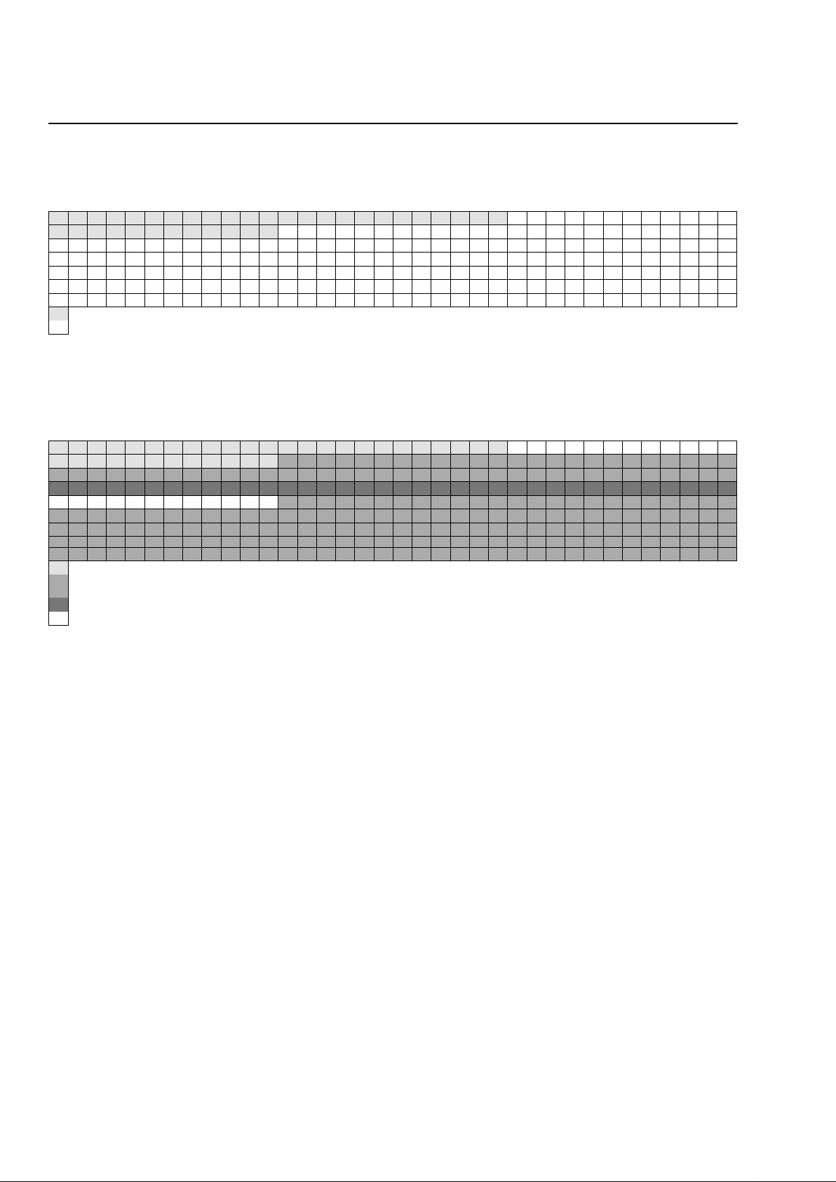
22 Agere Systems Inc.
Data Sheet
August 2001
Eight-Channel x 850 Mbits/s Backplane Transceiver
ORCA ORT8850 FPSC
Backplane Transceiver Core Detailed Description
(continued)
Table 2. Trans mitter TOH on LVDS Output (Transparent Mode)
In the TOH insert mode of operation, TOH bytes on LVDS output are shown in Table 3. This also shows the order
in which data is transferred to the serial TOH interface, starting with the most significant bit of the first A1 byte. The
first bit of the first byte is replaced by an even parity check bit over all TOH bytes from the previous TOH frame.
Table 3. Transmitter TOH on LVDS Output (TOH Insert Mode)
A1/A2 Frame Insert and Testing
The A1 and A2 bytes provide a special framing pattern that indicates where a STS-1 begins in a bit stream. All
12 A1 bytes of each STS-12 are set to 0xF6, and all 12 A2 bytes of the STS-12 are set to 0x28 when not overridden with an user-specified value for testing. The latency from the transmission of the first bit of the A1 byte at the
device output pins from the transmit frame pulse (SYS_FP) at the FPGA to embedded core input is between five to
seven cycles of fpga_sysclk.
A1/A2 testing (corruption) is controlled per stream by the A1/A2 error insert register. When A1/A2 corruption detection is set for a particular stream, the A1/A2 values in the corrupted A1/A2 value registers are sent for the number
of frames defined in the corrupted A1/A2 frame count register. When the corrupted A1/A2 frame count register is
set to zero, A1/A2 corruption will continue until the A1/A2 error insert register is cleared. This also allows alternate
values to be set for A1 and A2 during normal operation. For the ORT8850, it is optionally possible to not insert A1
and A2.
On a per-device basis, the A1 and A2 byte values are set, as well as the number of frames of corruption. Then, to
insert the specified A1/A2 values, each channel has an enable register. When the enable register is set, the A1/A2
values are corrupted for the number specified in the number of frames to corrupt. To insert errors again, the perchannel fault insert register must be cleared, and set again. Only the last A1 and the first A2 are corrupted.
A1 A1 A1 A1 A1 A1 A1 A1 A1 A1 A1 A1 A2 A2 A2 A2 A2 A2 A2 A2 A2 A2 A2 A2
B1 0 0 0 0 0 0 0 0 0 0 0
Regenerated bytes.
Transparent bytes from parallel input port.
A1 A1 A1 A1 A1 A1 A1 A1 A1 A1 A1 A1 A2 A2 A2 A2 A2 A2 A2 A2 A2 A2 A2 A2
B1 0 0 0 0 0 0 0 0 0 0 0 E1 E1 E1 E1 E1 E1 E1 E1 E1 E1 E1 E1 F1 F1 F1 F1 F1 F1 F1 F1 F1 F1 F1 F1
D1 D1 D1 D1 D1 D1 D1 D1 D1 D1 D1 D1 D2 D2 D2 D2 D2 D2 D2 D2 D2 D2 D2 D2 D3 D3 D3 D3 D3 D3 D3 D3 D3 D3 D3 D3
H1 H1 H1 H1 H1 H1 H1 H1 H1 H1 H1 H1 H2 H2 H2 H2 H2 H2 H2 H2 H2 H2 H2 H2 H3 H3 H3 H3 H3 H3 H3 H3 H3 H3 H3 H3
K1 K1 K1 K1 K1 K1 K1 K1 K1 K1 K1 K1 K2 K2 K2 K2 K2 K2 K2 K2 K2 K2 K2 K2
D4 D4 D4 D4 D4 D4 D4 D4 D4 D4 D4 D4 D5 D5 D5 D5 D5 D5 D5 D5 D5 D5 D5 D5 D6 D6 D6 D6 D6 D6 D6 D6 D6 D6 D6 D6
D7 D7 D7 D7 D7 D7 D7 D7 D7 D7 D7 D7 D8 D8 D8 D8 D8 D8 D8 D8 D8 D8 D8 D8 D9 D9 D9 D9 D9 D9 D9 D9 D9 D9 D9 D9
D10 D10 D10 D10 D10 D10 D10 D10 D10 D10 D10 D10 D11 D11 D11 D11 D11 D11 D11 D11 D11 D11 D11 D11 D12 D12 D12 D12 D12 D12 D12 D12 D12 D12 D12 D12
S1 S1 S1 S1 S1 S1 S1 S1 S1 S1 S1 S1
M0 M0 M0 M0 M0 M0 M0 M0 M0 M0 M0 M0
E2 E2 E2 E2 E2 E2 E2 E2 E2 E2 E2 E2
Regenerated bytes.
Inserted or transparent bytes. Blocks of 12 STS-1 bytes are controlled as a whole. There are 15 controls/channel: K1/K2, S1/M0, E1/F1/E2, D1, D2, D3, D4, D5, D6, D7, D8, D9, D10,
D11, D12.
Transparent bytes (from parallel input port).
Inserted bytes from TOH serial input port.

Agere Systems Inc. 23
Data Sheet
August 2001
Eight-Channel x 850 Mbits/s Backplane Transceiver
ORCA ORT8850 FPSC
Backplane Transceiver Core Detailed
Description
(continued)
B1 Calculation and Insertion
In a bit interleaved parity -8 (BIP-8) error check set for
even parity over all the bits of an STS-1 frame B1 is
defined for the first STS-1 in an STS-N only, the B1 calculation block computes a BIP-8 code, using even parity over all bits of the previous STS-12 frame after
scrambling and is inserted in the B1 byte of the current
STS-12 frame before scrambling. Per-bit B1 corruption
is controlled by the force BIP-8 corruption register (register address 0F). For any bit set in this register, the
corresponding bit in the calculated BIP-8 is inverted
before insertion into the B1 byte position. Each stream
has an independent fault insert register that enables
the inversion of the B1 bytes. B1 bytes in all other STS1s in the stream are filled with zeros. For the ORT8850,
it is optionally possible to not insert B1 and the subsequent 11 bytes of zeros.
Stream Disable
When disabled via the appropriate bit in the stream
enable register, the prescrambled data for a stream is
set to all ones, feeding the HSI. The HSI macro is powered down on a per-stream basis, as are its LVDS outputs.
Scrambler
The data stream is scrambled using a frame-synchronous scrambler with a sequence length of 127. The
scrambling function can be disabled by software. The
generating polynomial for the scrambler is 1 + x
6
+ x7.
This polynomial conforms to the standard SONET
STS-12 data format. The scrambler is reset to 1111111
on the first byte of the SPE (byte following the Z0 byte
in the twelfth STS-1). That byte and all subsequent
bytes to be scrambled are exclusive-ORed, with the
output from the byte-wise scrambler. The scrambler
runs continuously from that byte on throughout the
remainder of the frame. A1, A2, J0, and Z0 bytes are
not scrambled.
System Frame Pulse and Line Frame Pulse
System frame pulse (for transmitter) and line frame
pulse (for receiver) are generated in FPGA logic. A1/A2
framing is used on the link for locating the 8 kHz frame
location. All frames sent to the FPGA are aligned to the
FPGA frame pulse LINE_FP which is provided by the
FPGA to the STM macro. All frames sent from the
FPGA to the STM will be aligned to the frame pulse
SYS_FP that is supplied to the STM macro. In either
direction, the system frame pulse and line frame pulse
are active for one system clock cycle, indicating the
location of A1 byte of STS#1. They are common to all
eight channels except when the pointer mover and
alignment FIFOs are bypassed. In that case, a line
frame pulse for each receive channel is generated by
the STM macro and passed to the FPGA interface.
Repeater
This block is essentially the inverse of the sampler
block. It receives byte-wide STS-12 rate data from the
TOH insert block. In order to support the quad STS-1
and STS-3 modes of operation, the HSI (622 Mbits/s)
can be connected to a slower speed device (e.g.,
155 Mbits/s or 52 Mbits/s). The purpose of this block is
to rearrange the data being fed to the HSI so that each
bit is transmitted four or twelve times, thus simulating
155 Mbits/s or 51.84 Mbits/s serial data. For example,
in STS-3 mode, the incoming STS-12 stream is composed of four identical STS-3s so only every fourth
byte is used. The bit expansion process takes a single
byte and stretches it to take up 4 bytes each consisting
of
4 copies of the 8 bits from the original byte. In STS-1
mode, every twelfth byte is used and four groups of
3 bytes of the form AAAAAAAA, AAAABBBB, and
BBBBBBBB are forwarded to the HSI. An alternate
method for supplying STS-1 mode is to set the HSI to
run at 207.36 MHz and use the four times repeater
function.
STM Receiver (Backplane → FPGA)
Each of the two STM slices of the ORT8850 has four
receiving channels that can be treated as one STS-48
stream, or treated as independent channels. Incoming
data is received through LVDS serial ports at the data
rate of 622 Mbits/s. The receiver can handle the data
streams with frame offsets of up to ±12 bytes which
would be due to timing skews between cards and along
backplane traces or other transmission medium. In
order for this multichannel alignment capability to operate properly, it should be noted that while the skew
between channels can be very large, they must operate at the exact same frequency (0 ppm frequency
deviation), thus requiring that their transmitters be
driven by the same clock source. The received data
streams are processed in the HSI and the STM, and
then passed through the CIC boundary to the FPGA
logic.

2424 Agere Systems Inc.
Data Sheet
August 2001
Eight-Channel x 850 Mbits/s Backplane Transceiver
ORCA ORT8850 FPSC
Backplane Transceiver Core Detailed
Description
(continued)
Framer Block
The framer block takes byte-wide data from the HSI,
and outputs a byte-aligned, byte-wide data stream and
8 kHz sync pulse. The framer algorithm determines the
out-of-frame/in-frame status of the incoming data and
will cause interrupts on both an errored frame and an
out-of-frame (OOF) state. The framer detec ts the A1/
A2 framing pattern and generates the 8 kHz frame
pulse. When the framer detects OOF, it will generate
an interrupt. Also, the framer detects an errored frame
and increments an A1/A2 frame error counter. The
counter can be monitored by a processor to compile
performance status on the quality of the backplane.
Because the ORT8850 is intended for use between it
and another ORT8850 or other devices via a backplane, there is only one errored frame state. Thus, after
two transitions are missed, the state machine goes into
the OOF state and there is no severely errored frame
(SEF) or loss-of-frame (LOF) indication.
B1 Calculate
Each Rx block receives byte-wide scrambled
77.76 MHz data and a frame sync from the framer.
Since each HSI is independently clocked, the Rx block
operates on individual streams. Timing signals required
to locate overhead bytes to be extracted are generated
internally based on the frame sync. The Rx block produces byte-wide (optionally) descrambled data and an
output frame sync for the alignment FIFO block. The
frame sync signals are also sent to the FPGA logic for
use when the alignment FIFO block is bypassed.
The B1 calculation block computes a BIP-8 (bit interleaved parity 8 bits) code, using even parity over all bits
of the previous STS-12 frame before descrambling;
this value is checked against the B1 byte of the current
frame after descrambling. A per-stream B1 error
counter is incremented for each bit that is in error. The
error counter may be read via the CPU interface.
Descrambling.
The streams are descrambled using a
frame synchronous descrambler with a sequence
length of 127 with a generating polynomial of 1 + x
6
+
x
7
. The A1/A2 framing bytes, the section trace byte
(J0) and the growth bytes (Z0) are not descrambled.
The descrambling function can be disabled by software.
Sampler.
This block operates on the byte-wide data
directly from the HSI macro. The HSI external interface
always runs at 622 Mbits/s (STS-12), or 850 Mbits/s,
but it can be connected directly to a 155 Mbits/s STS-3
stream or a 51.84 Mbits/s STS-1 stream. If connected
to either a 155 Mbits/s or 51.84 Mbits/s stream, each
incoming data is received either 4 or 12 times respectively. This block is used to return the byte stream to
the expected STS-12 format. The mode of operation is
controlled by a register and can either be STS-12
(pass-through), STS-3 (every fourth bit), or STS-1
(every twelfth bit). The output from this block is not bitaligned (i.e., an 8-bit sample does not necessarily contain an entire SONET byte), but it is in standard
SONET STS-12 format (i.e., four STS-3s or 12 STS1s) and is suitable for framing.
AIS-L Insertion.
Alarm indication signal (AIS) is a continuous stream of unframed 1s sent to alert downstream equipment that the near-end term ina l has
failed, lost its signal source, or has been temporarily
taken out of service. If enabled in the AIS_L force register, AIS-L is inserted into the received frame by writing all ones for all bytes of the descrambled stream.
AIS-L Insertion on Out-of-Frame.
If enabled via a
register, AIS-L is inserted into the received frame by
writing all ones for all bytes of the descrambled stream
when the framer indicates that an out-of-frame condition exists.
Internal Parity Generation
Even parity is generated on all data bytes and is routed
in parallel with the data to be checked before the protection switch MUX at the parallel output.
Agere Systems Inc. 25
Data Sheet
August 2001
Eight-Channel x 850 Mbits/s Backplane Transceiver
ORCA ORT8850 FPSC
Backplane Transceiver Core Detailed Description
(continued)
Transport Overhead Extraction
Transport overhead is extracted from the receive data stream by the TOH extract block. The incoming data gets
loaded into a 36-byte shift register on the system clock domain. This, in turn, is clocked onto the TOH clock domain
at the start of the SPE time, where it can be clocked out.
During the SPE time, the receiver TOH frame pulse is generated, RX_TOH_FP, which indicates the start of the row
of 36 TOH bytes. This pulse, along with the receive TOH clock enable, RX_TOH_CK_EN, as well as the TOH data,
are all launched on the rising edge of the TOH clock TOH_CLK.
TOH Byte Ordering
The TOH processor is responsible for dropping all TOH bytes of each channel through one of four corresponding
serial ports. The four TOH serial ports are synchronized to the TOH clock (the same clock that is being used by the
serial ports on the transmitter side). This free-running TOH clock is provided to the core by external circuitry and
operates at a minimum frequency of 25 MHz and a maximum frequency of 77.76 MHz. Data is transferred over
serial links in a bursty fashion as controlled by the Rx TOH clock enable signal, which is generated by the ASIC
and common to the four channels. All TOH bytes of STS-12 streams are transferred over the appropriate serial link
in the same order in which they appear in a standard STS-12 frame. Data transfer should be preformed on a rowby-row basis such that internal data buffering needs is kept to a minimum. Data transfers on the serial links will be
synchronized relative to the Rx TOH frame signal.
Receiver TOH Reconstruction
Receiver TOH reconstruction on output parallel bus is as shown in the following table (if the pointer mover is not
bypassed).
Table 4. Receiver TOH (Output Parallel Bus)
On the TOH serial port, all TOH bytes are dropped as received on the LVDS input (MSB first). The only exception
is the most significant bit of byte A1 of STS#1, which is replaced with an even parity bit. This parity bit is calculated
over the previous TOH frame. Also, on AIS-L (either resulting from LOF or forced through software), all TOH bits
are forced to all ones with proper parity (parity automatically ends up being set to 1 on AIS-L).
Special TOH Byte Functions
K1 and K2 Handling.
The K1 and K2 bytes are used in automatic protection switch (APS) applications. K1 and K2
bytes can be optionally passed through the pointer mover under software control, or can be set to zero with the
other TOH bytes.
A1 and A2 Handling.
As discussed previously, the A1 and A2 bytes are used for a framing header. A1 and A2
bytes are always regenerated and set to hexadecimal F6 and 28, respectively.
A1 A1 A1 A1 A1 A1 A1 A1 A1 A1 A1 A1 A2 A2 A2 A2 A2 A2 A2 A2 A2 A2 A2 A2
000000000000
000000000000000000000000000000000000
000000000000000000000000000000000000
H1 H1 H1 H1 H1 H1 H1 H1 H1 H1 H1 H1 H2 H2 H2 H2 H2 H2 H2 H2 H2 H2 H2 H2 H3 H3 H3 H3 H3 H3 H3 H3 H3 H3 H3 H3
000000000000K100000000000K200000000000
000000000000000000000000000000000000
000000000000000000000000000000000000
000000000000000000000000000000000000
000000000000000000000000000000000000
Regenerated bytes.
Regenerated bytes (under pointer generator control, SS bits must be transparent, AIS-P must be supported).
Bytes taken from elastic store buffer, on negative stuff opportunity-else, forced to all zeros.
Transparent or all zeros (K1/K2 are either taken from K1/K2 buffer or forced to all zeros-soft, control). In transparent mode, AIS-L must be supported.
All zero bytes.
26 Agere Systems Inc.
Data Sheet
August 2001
Eight-Channel x 850 Mbits/s Backplane Transceiver
ORCA ORT8850 FPSC
Backplane Transceiver Core Detailed Description
(continued)
SPE and C1J1 Outputs
. These two signals for each channel are passed to the FPGA logic to allow a pointer processor or other function to extract payload without interpreting the pointers. For the ORT8850, each frame has
12 STS-1s. In the SPE region, there are 12 J1 pulses for each STS-1s. There is one C1(J0, new SONET specifications use J0 instead of C1 as section trace to identify each STS-1 in an STS-N) pulse in the TOH area for one
frame. Thus, there is a total of 12 J1 pulses and one C1(J0) pulse per frame. C1(J0) pulse is coincident with the J0
of STS1 #1. In each frame, the SPE flag is active when the data stream is in SPE area. SPE behavior is dependent
on pointer movement and concatenation. Note that in the TOH area, H3 can also carry valid data. When valid SPE
data is carried in this H3 slot, SPE is high in this particular TOH time slot. In the SPE region, if there is no valid data
during any SPE column, the SPE signal will be set to low. SPE allows a pointer processor to extract payload without interpreting the pointers. The SPE and C1J1 functionality are described in T able 5. For generic data operation,
valid data is available when SPE is 1 and the C1J1 signal is ignored.
Table 5
.
SPE and C1J1 Functionality
Note:The following rules are observed for generating SPE and C1J1 signals: on occurrence of AIS-P on any of the STS-1, there is no corre-
sponding J1 pulse. In case of concatenated payloads (up to STS48c), only the head STS-1 of the group has an associated J1 pulse.
C1J1 signal tracks any pointer movements. During a negative justification event, SPE is set high during the H3 byte to indicate that payload data is available. During a positive justification event, SPE is set low during the positive stuff opportunity byte to indicate that payload
data is not available.
5-9330(F)
Note:
C1J1 signal behavior shown in this figure is just for illustration purposes: C1 pulse position must always be as shown; however, position of J1
pulses vary based on path overhead location of each STS-1 within the STS-12 stream.
C1J1 signal must always be active during C1(J0) time slot of STS#1.
C1J1 signal must also be active during the twelve J1 time slots. However, C1J1 must not be active for any STS-1 for which AIS-P is generated.
Also, on concatenated payloads, only the head of the group must have a J1 pulse.
Figure 6. SPE and C1J1 Functionality
SPE C1J1 Description
0 0 TOH information excluding C1(J0) of STS1 #1.
0 1 Position of C1(J0) of STS1 #1 (one per frame). Typically used to provide a
unique link identification (256 possible unique links) to help ensure cards
are connected into the backplane correctly or cables are connected
correctly.
1 0 SPE information excluding the 12 J1 bytes.
1 1 Position of the 12 J1 bytes.
STS-12 TOH ROW # 1 SPE ROW # 1
A1 A1A1 A1 A1 A1A1 A1 A1 A1A1 A1 A2 A2A2 A2 A2 A2
A2 A2A2 A2 A2 A2 J0 Z0 Z0 Z0 Z0 Z0 Z0 Z0 Z0 Z0 Z0 Z0
STS-12
SPE
C1J1
C1 PULSE
J1 PULSE OF
3RD STS-1
first SPE BYTES OF THE
12 STS-1S
123456789101112
Agere Systems Inc. 27
Data Sheet
August 2001
Eight-Channel x 850 Mbits/s Backplane Transceiver
ORCA ORT8850 FPSC
Backplane Transceiver Core Detailed Description
(continued)
5-9331
Note:
SPE signal behavior shown in this figure is just for illustration purposes: SPE behavior is dependent on pointer movements and concatenation.
SPE signal must be high during negative stuff opportunity byte time slots (H3) for which valid data is carried (negative stuffing).
SPE signal must be low during positive stuff opportunity byte time slots for which there is no valid data (positive stuffing).
Figure 7. SPE Stuff Bytes
STM FIFO Alignment (Backplane
→
FPGA)
The alignment FIFO allows the transfer of all data to the system clock. The FIFO sync block (Figure 8) allows the
system to be configured to allow the frame alignment of multiple slightly varying data streams. This optional alignment ensures that matching STS-12 streams will arrive at the FPGA end in perfect data sync. The frame alignment
is configurable to allow for the possibility of fully independent (i.e., total frame misalignment) STS-12s.
STS-12 TOH ROW # 4 SPE ROW # 4
H1H1 H1H1H1 H1H1H1 H1H1 H1 H1H2 H2H2H2 H2H2
H2H2 H2H2H2 H2H3H3 H3H3 H3H3H3 H3H3H3 H3H3
STS-12
SPE
POSITIVE STUFF
OPPORTUNIT Y BYTES
123456789101112
NEGATIVE STUFF
OPPORTUNITY BYTES
SPE SIGNAL SHOWS NEGATIVE STUFFING FOR 2ND STS-1,
AND POSITIVE STUFFING FOR 6TH STS-1
2828 Agere Systems Inc.
Data Sheet
August 2001
Eight-Channel x 850 Mbits/s Backplane Transceiver
ORCA ORT8850 FPSC
Backplane Transceiver Core Detailed
Description
(continued)
5-8577 (F)
Figure 8. Interconnect of Streams for FIFO
Alignment
The incoming data from the HSI (also referred to as
CDRM850) can be separated into four STS-12 channels (A, B, C, and D) per slice. Thus, there are STS-12
channels AA to AD from slice A of the STM and STS12 channels BA to BD of slice B. These streams can be
frame-aligned in the following patterns: in STS-48
mode, all four STS-12s of each STM slice are aligned
with each other (i.e., AA, AB, AC, AD). Optionally, in
STS-48 mode, all eight STS-12s (STMs A and B) can
be aligned (to allow hitless switching at the STS-48
level). Multiple devices can be aligned to enable STS192 or higher modes. Streams can also be aligned on a
twin STS-12 basis. There is also a provision to allow
certain stre ams t o be dis abl ed (i. e. , not pr oduc ing inte rrupts or affecting synchronization). These streams can
be enabled at a later time without disrupting other
streams. If the selected stream needs to be a part of a
bigger group (i.e., STM A), then either the entire group
must be resynched or the affected stream must have
been in the correct mode (i.e., align all STM A) when
the initial synchronization was performed. As long as
all four streams in STM A are in the correct mode when
synchronization takes place, then those streams may
be enabled or disabled without affecting synchronization.
These streams can be frame-aligned in the patterns
shown in Figure 10, Figure 9, and Figure 11.
0674
Figure 9. Example of Inter-STM Alignment
0673(F)
Figure 10. Example of Intra-STM Alignment
0675
Figure 11. Example of Twin STS-12 Stream
Alignment
STS-12
STREAM AA
STS-12
STREAM AB
STS-12
STREAM AC
STS-12
STREAM AD
STS-12
STREAM BA
STS-12
STREAM BB
STS-12
STREAM BC
FIFO
SYNC
STS-12
STREAM BD
STM SLICE A
STM SLICE B
STM A Stream A
STM A Stream B
STM A Stream C
STM A Stream D
STM B Stream A
STM B Stream B
STM B Stream C
STM B Stream D
ALL 8 ALIGNMENT OF STM A AND STM B
STM A Stream A
STM A Stream B
STM A Stream C
STM A Stream D
STM B Stream A
STM B Stream B
STM B Stream C
STM B Stream D
t
0
STM A Stream A
STM A Stream B
STM A Stream C
STM A Stream D
STM B Stream A
STM B Stream B
STM B Stream C
STM B Stream D
ALL 4 ALIGNMENT OF STM A AND STM B
STM A Stream A
STM A Stream B
STM A Stream C
STM A Stream D
STM B Stream A
STM B Stream B
STM B Stream C
STM B Stream D
t
0
t
1
STM A Stream A
STM A Stream B
STM A Stream C
STM A Stream D
STM B Stream A
STM B Stream B
STM B Stream C
STM B Stream D
TWINS ALIGNMENT OF STR EAMS A AND C
t
0
STM A Stream A
STM B Stream A
STM B Stream B
STM B Stream C
STM B Stream D
t
1
STM A Stream B
STM A Stream D
STM A Stream C

Agere Systems Inc. 29
Data Sheet
August 2001
Eight-Channel x 850 Mbits/s Backplane Transceiver
ORCA ORT8850 FPSC
Backplane Transceiver Core Detailed
Description
(continued)
The FIFO block consists of a 24-bit by 10-bit FIFO per
link. This FIFO is used to align up to ±154.3 ns of interlink skew and to transfer to the system clock. The FIFO
sync circuit takes metastable hardened frame pulses
from the write control blocks and produces sync signals
that indicate when the read control blocks should begin
reading from the first FIFO location. On top of the sync
signals, this block produces an error indicator which
indicates that the signals to be aligned are too far apart
for alignment (i.e., greater than 18 clocks apart). Sync
and error signals are sent to read control block for
alignment. The read control block is synched only once
on start-up; any further synchroni z ati on is softwar e
controlled. The action of resynching a read control
block will always cause loss of data. A register allows
the read control block to be resynched.
STM Link Alignment
The general operation of the link alignment algorithm is
to wait 12 clocks (i.e., half the FIFO) from the arriving
frame pulse and then signal the read control block to
begin reading. For perfectly aligned frame pulses
across the links, it is simply a matter of counting down
12 and then signaling the read control block .
The algorithm down counts by one until all of the frame
pulses have arrived and then by two when they are all
present. For example (Figure 12), if all pulses arrive
together, then alignment algorithm would count 24
(12 clocks); if, however, the arriving pulses are spread
out over four clocks, then it would count one for the first
four pulses and then two per clock afterward, which
gives a total of 14 clocks between first frame pulse and
the first read. This puts the center of arriving frame
pulses at the halfway point in the buffer. This is the
extent of the algorithm, and it has no facility for actively
correcting problems once they occur.
The write control block receives byte-wide data at
77.76 MHz and a frame pulse two clocks before the
first A1 byte of the STS-12 frame. It generates the write
address for the FIFO block. The first A1 in every STS12 stream is w ritte n in the s ame lo catio n (add ress 0) in
the FIFO. Also, a frame bit is passed through the FIFO
along with the first byte before the first A1 of the STS-
12. The read control block synchronizes the reading of
the FIFO for streams that are to be aligned. Reading
begins when the FIFO sync signals that all of the applicable A1s and the appropriate margin have been written to the FIFO. All of the read blocks to be
synchronized begin reading at the same time and
same location in memory (address 0).
The alignment algorithm takes the difference between
read address and write address to indicate the relative
clock alignments between STS-12 streams. If this
depth indication exceeds certain limits (12 clocks),
then an interrupt is given to the microprocessor (alignment overflow). Each STS-12 stream can be realigned
by software if it gets too far out of line (this would
cause a loss of data). For background applications that
have less than 154.3 ns of interlink skew, misalignment
will not occur.
STM Link Alignment Setup
In order to ensure proper operation of the STM Link
Alignment capability, the following setup procedures
should be followed after the enabled channels have a
valid frame pulse:
1. Put all of the streams to be aligned, including disabled streams, into their required alignment mode.
2. Force AIS-L in all streams to be synchronized
(refer to register map, write 0x01 to DB6 or register
0x30020, 0x30038, 0x30050, 0x30068, 0x30080,
0x30098, 0x300B0, and 0x300C8).
3. Wait four frames. Write a 0x01 to the FIFO alignment resync register bits as required in register
0x30017 or 0x30018. Wait four frames.
4. Release the AIS-L in all streams (write 0x00 to
DB6 or register 0x30020, 0x30038, 0x30050,
0x30068, 0x30080, 0x30098, 0x300B0, and
0x300C8). This procedure allows normal data flow
through the embedded core.
5-8584 (F)
Figure 12. Examples of Link Alignment
24-byte
FIFO
24-byte
FIFO
ALL FPs
12 CLO C K S
SYNC. PULSEARRIVE
TOGETHER
(WRITING
BEGINS)
(READING
BEGINS)
SYNC PULSE
(READING
BEGINS)
LAST FP
ARRIVES
4 CLOCK S
FIRST FP
ARRIVES
(W R IT IN G
BEGINS)
10 CLO C K S
PERFECTLY ALIGNED FRAMES 4-BYTE SPREAD IN ARRIVING FRAMES

30 Agere Systems Inc.
Data Sheet
August 2001
Eight-Channel x 850 Mbits/s Backplane Transceiver
ORCA ORT8850 FPSC
Backplane Transceiver Core Detailed Description
(continued)
8B/10B Transmitter (FPGA → Backplane)
For each channel, an 8B/10B encoder can be enabled in place of the STM transmitter. This block receives 8-bit
data from the FPGA interface, encodes it into a 10-bit code, and then sends this 10-bit code to the HSI block for
serialization and transmission from the ORT8850. This 8-bit to 10-bit encoding provides for guaranteed transmission of a large number of transmissions to allow for easy recovery by a CDR on the other end of the backplane or
transmission medium, and also allows for the insertion of control characters. These control characters have many
uses, including their use in the ORT8850 to align 10-bit word boundries and perform multi-channel alignments, as
will be discussed in the 8B/10B receiver section.
The data input to the transmitter of each channel from the FPGA logic is an 8-bit word and K-control input. The Kcontrol input is used to designate data or a special character, where a logic 1 indicates that the data should be
mapped to a control character. The following table shows this mapping that is supported. Two different codings are
possible for each data value and are shown as encoded word (+) and encoded word (–). The transmitter selects
between the positive or negative encoded word based on the calculated disparity of the present data.
Table 6. Valid Special Characters
It should also be noted that the data is serialized in the reverse order from the STM block, where dinxy[0] is transmitted first (the 8B/10B receive block also deserializes in the reverse order of the STM receive block).
8B/10B Receiver (Backplane → FPGA)
Instead of using the STM receiver block in the ORT8850, a separate decoder block is available to allow for receiving data that has been encoded using a standard 8B/10B encoder. This encoding/decoding scheme also allows for
the transmission of special characters and allows for error detection.
Clock recover for the 8B/10B decoder is performed by the HSI block for each of the eight receive channels in the
ORT8850. This recovered data is then aligned to a 10-bit word boundry by detecting and aligning to the commacodeword. Word alignment is done to either polarity of this codeword. The 10-bit code word is passed to the
decoder, which provides an 8-bit byte of data and a COMMADET signal to the multi-channel alignment block. In
8B/10B mode, the receiver can handle ± 12 bytes of skew between channels which would be due to timing skews
between cards and along backplane trace or other transmission medium. In order for this multi-channel alignment
capability to operate properly, it should be noted that while the skew between channels can be very large, they
must operate at the exact same frequency (0 ppm frequency deviation), thus requiring their transmitters to be
driven by the same clock source. This alignment FIFO can be bypassed. The COMMADET signal is also provided
to the FPGA logic per channel on the signal doutxy_fp, where x designates either four-channel macro A or B, while
y designates the channel (A, B, C, D) in each macro.
K character
HGF EDCBA
765 43210
K control
Encoded Word (–) Encoded Word (+)
abcdei fghj abcdei fghj
K28.0 000 11100 1 001111 0100 110000 1011
K28.1 001 11100 1 001111 1001 110000 0110
K28.2 010 11100 1 001111 0101 110000 1010
K28.3 011 11100 1 001111 0011 110000 1100
K28.4 100 11100 1 001111 0010 110000 1101
K28.5 101 11100 1 001111 1010 110000 0101
K28.6 110 11100 1 001111 0110 110000 1001
K28.7 111 11100 1 001111 1000 110000 0111
K23.7 111 10111 1 111010 1000 000101 0111
K27.7 111 11011 1 110110 1000 001001 0111
K29.7 111 11101 1 101110 1000 010001 0111
K30.7 111 11110 1 011110 1000 100001 0111
 Loading...