

AGERE ORT82G5-3BM680, ORT82G5-2BM680, ORT82G5-1BM680 Datasheet
Preliminary Data Sheet
July 2001
ORCA
®
ORT82G5 1.0—1.25/2.0—2.5/3.125 Gbits/s
Backplane Interface FPSC
Introduction
Agere Systems Inc. has developed a next generation
FPSC intended for high-speed serial backplane data
transmission. Built on the Ser ies 4 reco nfi gurable
embedded system-on-chips (SoC) architecture, the
ORT82G5 is made up of backplane transceivers containing eight channels, each operating at up to
3.125 Gbits/s (2.5 Gbits/s data rate), with a fullduplex synchronous interface with built-in clock and
data recovery (CDR), along with up to 400k usable
FPGA system gates. The CDR circuitry is a macrocell available from Agere's smart silicon macro
library, and has already been implemented in numerous applications including ASICs, standard products,
and FPSCs to create interfaces for SONET/SDH,
STS-48/STM-16, STS-192/STM-64, and 10 Gbit
Ethernet applications. With the addition of protocol
and access logic such as protocol-independent framers, asynchronous transfer mode (ATM) framers,
packet-over-SONET (POS) interfaces, and framers
for HDLC for Internet protocol (IP), designers can
build a configurable interface retaining proven backplane driver/receiver technology. Designers can also
use the device to drive high-speed data transfer
across buses within a system that are not SONET/
SDH based. For example, designers can build a 20
Gbits/s bridge for 10 Gbits/s Ethernet; the high-
speed SERDES interfaces can comprise two XAUI
interfaces with configurable back-end interfaces such
as XGMII or POS-PHY4. The ORT82G5 can also be
used to provide a full 10 Gbits/s backplane data connection with protection between a line card and
switch fabric.
The ORT82G5 offers a clockless high-speed interface for interdevice communication on a board or
across a backplane. The built-in clock recovery of the
ORT82G5 allows for higher system performance,
easier-to-design clock domains in a multiboard system, and fewer signals on the backplane. Network
designers will benefit from the backplane transceiver
as a network termination device.The first version of
the device supports 8b/10b encoding/decoding and
link state machines for Ethernet, fibre-channel, and
InfiniBand
™. Version II adds SONET data scrambling/descrambling, streamlined SONET framing,
transport overhead handling, plus the programmable
logic to terminate the network into proprietary systems. For non-SONET applications, all SONET functionality is hidden from the user and no prior
networking knowledge is required.
Version II adds decimation and interpolation for connections at 622 Mbits/s rates.
Table 1.
ORCA
ORT82G5 Family—Available FPGA Logic
† The embedded core and interface are not included in the above gate counts. The usable gate counts range from a logic-only gate count
to a gate count assuming that 20% of the PFUs/SLICs are being used as RAMs. The logic-only gate count includes each PFU/SLIC
(counted as 108 gates/PFU), including 12 gates per LUT/FF pair (eight per PFU), and 12 gates per SLIC/FF pair (one per PFU). Each of
the four PIO groups are counted as 16 gates (three FFs, fast-capture latch, output logic, CLK, and I/O buffers). PFUs used as RAM are
counted at four gates per bit, with each PFU capable of implementing a 32 x 4 RAM (or 512 gates) per PFU. Embedded block RAM
(EBR) is counted as four gates per bit plus each block has an additional 25k gates. 7k gates are used for each PLL and 50k gates for the
embedded system bus and microprocessor interface logic. Both the EBR and PLLs are conservatively utilized in the gate count calculations.
‡ 372 user I/Os out of a total of 432 user I/Os are bonded in the 680 PBGAM package.
Device
PFU
Rows
PFU
Columns
Total
PFUs
User I/O LUTs
EBR
Blocks
EBR Bits
(k)
Usable
†
Gates (k)
ORT82G5 36 36 1296 372/432
‡
10,368 12 111 380—800

Table of Contents
Contents Page Contents Page
2 Agere Systems Inc.
Preliminary Data Sheet
July 2001
1.0-1.25/2.0-2.5/3.125 Gbits/s Backplane Interface
ORCA
ORT82G5 FPSC Eight-Channel
Introduction..................................................................1
Embedded Function Features .....................................4
Intellectual Property Features......................................4
Programmable Features..............................................5
Programmable Logic System Features .......................6
Description...................................................................7
What Is an FPSC? ....................................................7
FPSC Overview .........................................................7
FPSC Gate Counting ................................................7
FPGA/Embedded Core Interface ..............................7
ORCA Foundry 2000 Development System ........... .. 7
FPSC Design Kit .......................................................8
FPGA Logic Overview ...............................................8
PLC Logic ..................................................................8
Programmable I/O .....................................................9
Routing ....................... ............................................... 9
System-Level Features..............................................10
Microprocessor Interface .........................................10
System Bus ................................... ...... ....... .............10
Phase-Locked Loops ..............................................10
Embedded Block RAM ............................................10
Configuration .............. .............................................11
Additional Information ............ ....... ...... ....... ...... .......11
ORT82G5 Overview ..................................................11
Device Layout .........................................................11
Backplane Transceiver Interface .............................11
ORT82G5 Overview (continued)...............................12
Serializer and Deserializer (SERDES) ....................14
MUX/DeMUX Block .................................................14
Multichannel Alignment FIFOs ................................14
XAUI or Fibre-Channel Link State Machine ............14
Dual Port RAMs ......................................................14
FPGA Interface .......................................................15
FPSC Configuration ................................................15
Backplane Transceiver Core Detailed Description....15
SERDES .................................................................15
SERDES Transmit Path (FPGA Æ Backplane) ......18
Transmit Preemphasis and Amplitude Control ........19
SERDES Receive Path (Backplane Æ FPGA) .......19
8b/10b Encoding/Decoding ........... ...... ....... ...... .......21
SERDES Transmit and Receive PLLs ................... 21
Reference Clock ..................................................... 21
Byte Alignment ....................................................... 22
Link State Machines ............................................... 22
XAUI Link Synchronization Function ...................... 23
MUX/DeMUX Block ................................................ 25
Multichannel Alignmen t (Ba ckpl ane Æ FPGA) ....... 27
Alignment Sequence .............................................. 29
Loopback Modes .................................................... 32
High-Speed Serial Loopback .................................. 32
Parallel Loopback at the SERDES Boundary ......... 33
Parallel Loopback at MUX/DeMUX Boundary
Excluding SERDES ............................................... 33
ASB Memory Blocks .................. ....... ...... ....... ...... ... 34
Memory Map............................................................. 36
Definition of Register Types ................................... 36
Absolute Maximum Ratings...................................... 54
Recommended Operating Conditions ...................... 54
HSI Electrical and Timing Characteristics ................ 54
Pin Information ......................................................... 57
Power Supplies for ORT82G5 ................................ 63
Recommended Power Supply Connections ........... 64
Recommended Power Supply Filtering Scheme .... 64
Package Pinouts .................................................... 69
Pin Information ......................................................... 70
Package Thermal Characteristics
Summary.................................................................. 87
Θ
JA ................................................... ...... ....... ...... ... 87
ψ
JC ........................................................................ 87
Θ
JC ........................................................................ 87
Θ
JB ........................................................................ 87
FPSC Maximum Junction Temperature ................. 87
Package Thermal Characteristics............................. 88
Package Coplanarity ................................................ 88
Package Parasitics................................................... 88
Package Outline Diagrams....................................... 89
Terms and Definitions ............................................ 89
680-Pin PBGAM ..................................................... 90
Hardware Ordering Information................................ 91
Software Ordering Information ................................. 91

Agere Systems Inc. 3
Preliminary Data Sheet
July 2001
1.0-1.25/2.0-2.5/3.1 25 Gbit s/s Backplane Interface
ORCA ORT82G5 FPSC Eight-Channel
Table of Contents
List of Figures Page List of Tables Page
Figure 1. ORT82G5 Block Diagram ..........................12
Figure 2. Internal High-Level Diagram of ORT82G5
Transceiver ..............................................................13
Figure 3. SERDES Functional Block Diagram for
One Channel ...........................................................17
Figure 4. ORT82G5 Transmit Path for a Single
SERDES Channel ...................................................18
Figure 5. ORT82G5 Receive Path for a Single
SERDES Channel ...................................................20
Figure 6. Fibre-Channel Link State Machine State
Diagram ............................ ................................ .......22
Figure 7. XAUI Link Synchronization State
Diagram ............................ ................................ .......24
Figure 8. Transmit MUX Block for a Single SERDES
Channel ............................ .......................................25
Figure 9. Receive DeMUX Block for a Single
SERDES Channel ...................................................26
Figure 10. Interconnect of Streams for FIFO ............27
Figure 11. Example of SERDES A Alignment and ...27
Figure 12. Example of SERDES A and B
Alignment ................................................................27
Figure 13. Example of Multiple Twin Channel ..........27
Figure 14. Multichannel Alignment FIFO Block for
a Single SERDES Channel .....................................28
Figure 15. De-Skew Lanes by Aligning /A/
Columns ..................................................................30
Figure 16. Block Diagram of Memory Block .............34
Figure 17. Minimum Timing Specs for Memory
Blocks-Write Cycle ..................................................35
Figure 18. Minimum Timing Specs for Memory
Blocks-Read Cycle ..................................................35
Figure 19. Receive Data Eye-diagram Template
(Differential) ...................... .......................... .............55
Figure 20. Power Supply Filtering ............................65
Figure 21. Package Parasitics ..................................88
Table 1.
ORCA
ORT82G5 Family—Available
FPGA Logic ...............................................................1
Table 2. Preemphasis Settings ...................................19
Table 3. Tr ansmi t PLL Clock and Data Rates ............21
Table 4. Receive PLL Clock and D at a R ates .............21
Table 5. XAUI Link Synchronizat ion State
Diagram Notation—Variables ..................................23
Table 6. XAUI Link Synchronizat ion State
Diagram—Functions ................................................23
Table 7. Multichannel Alignment Modes ................ .....29
Table 8. Definition of Bits of MRWDxy[39:0] ...............31
Table 9. High-Speed Serial Loopback Configuration .32
Table 10. Parallel Loopback Co nf iguration .......... . ... ...33
Table 11. Structural Register Elements ......................36
Table 12. Memory Map ...............................................37
Table 13. Absolute Maximum Ratings ........................54
Table 14. Recommended Operating Conditions ........54
Table 15. Absolute Maximum Ratings ........................54
Table 16. Recommended Operating Conditions ........54
Table 17. Receiver Specifications ..............................55
Table 18. Reference Clock Spec if ic at ions
(REFINP and REFINN) ............................................56
Table 19. Channel Output Jitter (1.25 Gbits/s) ........... 56
Table 20. Channel Output Jitter (2.5 Gbits/s) .............56
Table 21. Serial Output Timing Levels (CML I/ O) ... . ...56
Table 22. Serial Input Timing and Levels (CML I/O) ...56
Table 23. FPGA Common-Fun c tio n Pin
Description
..57
Table 24. FPSC Function Pin D es c ript ion ..... ... ... . ... ...60
Table 25. Power Supply Pin Groupings ......................63
Table 26. Embedded Core/FPGA Interface
Signal Description ...................................................66
Table 27. ORT82G5 680-Pin PBGAM Pinout ...... . ... ...70
Table 28.
ORCA
ORT82G5 Plastic Package
Thermal Guidelines .................................................88
Table 29.
ORCA
ORT82G5 Package Parasitics ........88
Table 30. Device Type Options ..................................91
Table 31. Temperature Options ..................................91
Table 32. Package Type Options ...............................91
Table 33.
ORCA
FPSC Package Matrix
(Speed Grades) .......................................................91

44 Agere Systems Inc.
Preliminary Data Sheet
July 2001
1.0-1.25/2.0-2.5/3.125 Gbits/s Backplane Interface
ORCA ORT82G5 FPSC Eight-Channel
Embedded Function Features
■
High-speed SERDES programmable serial data
rates of 622 Mbits/s (SONET only), 1.25 Gbits/s,
2.5 Gbits/s, and 3.125 Gbits/s.
■
Asynchronous operation per receive channel with the
receiver frequency tolerance based on one reference
clock per quad channels (separate PLL per channel).
■
Ability to select full-rate or half-rate operation per Tx
or Rx channel by setting the appropriate control registers.
■
Transmit preemphasis (programmable) for improved
receive data eye opening.
■
Receiver energy detector to determine if a link is
active.
■
32-bit (SONET or 8b/10b) or 40-bit (raw data) parallel internal bus for data processing in FPGA logic.
■
Provides a 10 Gbits/s backplane interface to switch
fabric with protection. Also supports port cards at
622 Mbits/s or 2.5 Gbits/s.
■
3.125 Gbits/s SERDES compliant with XAUI serial
data specification for 10 Gbit Ethernet applications
with protection.
■
Most XAUI f eatures for 10 Gbit Ethernet are embedded including the required link state machine.
■
Compliant to fibre-channel physical layer specification.
■
Allows wide range of applications for SONET network termination, as well as generic data moving for
high-speed backplane data transfer.
■
No knowledge of SONET/SDH needed in generic
applications. Simply supply data, a 100 MHz—
156.25 MHz reference clock, and, optionally, a frame
pulse.
■
High-speed interface (HSI) function for clock/data
recovery serial backplane data transfer without external clocks.
■
Eight-channel HSI function provides 2.5 Gbits/s
serial user data interface per channel for a total chip
bandwidth of 20 Gbits/s (full duplex).
■
SERDES has low-power CML buffers. Support for
1.5 V/1.8 V I/Os.
■
Programmable STS-12 or STS-48 framing in SONET
mode per channel (in version II). OC-192 framing in
quad OC-48 (four channels) also supported.
■
Powerdown option of SERDES HSI receiver on a
per-channel basis.
■
Selectable 8b/10b coder/decoder or SONET scrambler/descrambler (added for version 2).
■
SERDES HSI automatically recovers from loss-ofclock once its reference clock returns to normal operating state.
■
In-band management and configuration thr oug h
transport overhead extraction/insertion in SONET
mode (version II).
■
Supports transparent mode where the only insertion
is A1/A2 framing bytes in SONET mode (version II).
■
Built-in boundary scan (IEEE® 1149.1 and 1149.2
JTAG) for the programmable I/Os, not including the
SERDES interface.
■
FIFOs align incoming data across all eight channels
(all eight channels, two groups of four channels, or
four groups of two channels). Alignment is done
using comma characters or /A/ in 8b/10b mode or
frame pulse in SONET mode (version II). Optional
ability to bypass alignment FIFOs for asynchronous
operation between channels. (Each channel includes
its own clock and frame pulse or comma detect.)
■
Frame alignment across multiple ORT82G5 devices
for work/protect switching at STS-768/STM256 and
above rates in SONET mode.
■
Addition of two 4K X 36 dual-port RAMs with access
to the programmable logic.
Intellectual Property Features
Programmable logic provides a variety of yet-to-be
standardized interface functions, including the following
Agere ME IP core functions:
■
10 Gbits/s Ethernet as defined by IEEE 802.3ae:
— XGMII for interfacing to 10 Gbits/s Ethernet
MACs. XGMII is a 156 MHz double data rate parallel short reach (typically less than 2") interconnect interface.
— X
58
+ X39 + X1 scrambler/descrambler for
10 Gbits/s Ethernet.
— 64b/66b encoders/decoders for 10 Gbits/s Ether-
net.
— XAUI to XGMII translator, including dual XAUI pro-
tection.
■
POS-PHY4 inter fac e f or 10 Gbits/ s SONET/SDH and
OTN systems and some 10 Gbits/s Ethernet systems
to allow easy integration of InfiniBand, fibre-channel,
and 10 Gbits/s Ethernet in data over fibre applications.
■
Ethernet MAC functions at 10/100 Mbits/s, 1 Gbits/s,
and 10 Gbits/s.
■
Other functions such as fibre-channel and InfiniBand
link layer IP cores are also going to be developed.

Agere Systems Inc. 5
Preliminary Data Sheet
July 2001
1.0-1.25/2.0-2.5/3.1 25 Gbit s/s Backplane Interface
ORCA ORT82G5 FPSC Eight-Channel
Programmable Features
■
High-performance programmable logic:
— 0.13 µm 7-level metal technology.
— Internal performance of >250 MHz.
— Over 400k usable system gates.
— Meets multiple I/O interface standards.
— 1.5 V operation (30% less power than 1.8 V oper-
ation) translates to greater performance.
■
Traditional I/O selections:
— LVTTL and LVCMOS (3.3 V, 2.5 V, and 1.8 V) I/Os.
— Per pin-selectable I/O clamping diodes provide
3.3 V PCI compliance.
— Individually programmable drive capability:
24 mA sink/12 mA source, 12 mA sink/6 mA
source, or 6 mA sink/3 mA source.
— Two slew rates supported (fast and slew-limited).
— Fast-capture input latch and input flip-flop
(FF)/latch for reduced input setup time and zero
hold time.
— Fast open-drain drive capability.
— Capability to register 3-state enable signal.
— Off-chip clock drive capability.
— Two-input function generator in output path.
■
New programmable high-speed I/O:
— Single-ended: GTL, GTL+, PECL, SSTL3/2
(class I and II), HSTL (Class I, III, IV), ZBT, and
DDR.
— Double-ended: LVDS, bused-LVDS, and LVPECL.
Programmable, parallel termination (100 Ω) is
also supported for these I/Os.
— Customer defined: ability to substitute arbitrary
standard cell I/O to meet fast-moving standards.
■
New capability to (de)multiplex I/O signals:
— New DDR on both input and output at rates up to
311 MHz (622 MHz effective rate).
— New 2x and 4x downlink and uplink capability per
I/O (i.e., 50 MHz internal to 200 MHz I/O).
■
Enhanced twin-quad programmable function unit
(PFU):
— Eight 16-bit look-up tables (LUTs) per PFU.
— Nine user registers per PFU, one following each
LUT, and organized to allow two nibbles to act
independently, plus one e xtr a f or arithmetic operations.
— New register control in each PFU has two inde-
pendent programmable clocks, clock enables,
local set/reset, and data selects.
— New LUT structure allows flexible combinations of
LUT4, LUT5, new LUT6, 4
→
1 MUX, new
8 → 1 MUX, and ripple mode arithmetic functions
in the same PFU.
— 32 x 4 RAM per PFU, configurable as single- or
dual-port. Create large, fast RAM/ROM blocks
(128 x 8 in only eight PFUs) using the SLIC
decoders as bank drivers.
— Soft-wired LU Ts (S WL) al lo w fast cascadin g of up
to three levels of LUT logic in a single PFU
through fast internal routing which reduces routing congestion and improves speed.
— Flexible fast access to PFU inputs from routing.
— Fast-carry logic and routing to all four adjacent
PFUs for nibble-wide, byte-wide, or longer arithmetic functions, with the option to register the
PFU carr y -o ut.
■
Abundant high-speed buffered and nonbuffered routing resources provide 2x average speed improvements over previous architectures.
■
Hierarchical routing optimized for both local and global routing with dedicated routing resources. This
results in faster routing times with predictable and
efficient performance.
■
SLIC provides eight 3-statable buffers, up to a 10-bit
decoder, and PAL™-like and-or-invert (AOI) in each
programmable logic cell.
■
New 200 MHz embedded quad-port RAM blocks,
2 read ports, 2 write ports, and 2 sets of byte lane
enables. Each embedded RAM block can be configured as:
— 1—512 x 18 (quad-port, two read/two write) with
optional built in arbitration.
— 1—256 x 36 (dual-port, one read/one write).
— 1—1k x 9 (dual-port, one read/one write).
— 2—512 x 9 (dual-port, one read/one write for
each).
— 2 RAMS with arbitrary number of words whose
sum is 512 or less by 18 (dual-port, one read/one
write).
— Supports joining of RAM blocks.
— Two 16 x 8-bit content addressable memory
(CAM) support.
— FIFO 512 x 18, 256 x 36, 1k x 9, or dual 512 x 9.
— Constant multiply (8 x 16 or 16 x 8).
— Dual variable multiply (8 x 8).
■
Embedded 32-bit internal system bus plus 4-bit parity interconnects FPGA logic, microprocessor interface (MPI), embedded RAM blocks, and embedded
standard cell blocks with 66 MHz bus performance.
Included are built-in system registers that act as the
control and status center for the device.

66 Agere Systems Inc.
Preliminary Data Sheet
July 2001
1.0-1.25/2.0-2.5/3.125 Gbits/s Backplane Interface
ORCA ORT82G5 FPSC Eight-Channel
Programmable Features
(continued)
■
Built-in testability:
— Full boundary scan (IEEE 1149.1 and Draft
1149.2 JTAG).
— Programming and readback through boundary
scan port compliant to IEEE Draft 1532:D1.7.
— TS_ALL testability function to 3-state all I/O pins.
— New temperature-sensing diode.
■
Improved built-in clock management with programmable phase-locked loops (PPLLs) provide optimum
clock modification and conditioning for phase, frequency, and duty cycle from 20 MHz up to 420 MHz.
■
New cycle stealing capability allows a typical 15% to
40% internal speed improvement after final place
and route. This feature also enables compliance with
many setup/hold and clock to out I/O specifications
and may provide reduced ground bounce for output
buses by allowing flexible delays of switching output
buffers.
Programmable Logic System Features
■
PCI local bus compliant for FPGA I/Os.
■
Improved PowerPC®860 and PowerPC II high speed synchronous microprocessor interface can be
used for configuration, readback, device control, and
device status, as well as for a general-purpose interface to the FPGA logic, RAMs, and embedded standard cell blocks. Glueless interface to synchronous
PowerPC processors with user-configurable address
space provided.
■
New embedded AMBA™ specification 2.0 AHB system bus (ARM
®
processor) facilitates communication among the microprocessor interface,
configuration logic, embedded block RAM, FPGA
logic, and embedded standard cell blocks.
■
New network PLLs meet ITU-T G.811 specifications
and provide clock conditioning for DS-1/E-1 and
STS-3/ST M-1 applications.
■
Flexible general purpose PPLLs offer clock multiply
(up to 8x), divide (down to 1/8x), phase shift, delay
compensation, and duty cycle adjustment combined.
■
Variable size bused readback of configuration data
capability with the built-in microprocessor interface
and system bus.
■
Internal, 3-state, and bidirectional buses with simple
control provided by the SLIC.
■
New clock routing structures for global and local
clocking significantly increases speed and reduces
skew (<200 ps for OR4E4).
■
New local clock routing structures allow creation of
localized clock trees.
■
New double-data rate (DDR) and zero-bus turnaround (ZBT) memory interfaces support the latest
high-speed memory interfaces.
■
New 2x/4x uplink and downlink I/O capabilities inter face high-speed external I/Os to reduced speed
internal logic.
■
ORCA Foundry 2000 development system software.
Supported by industry-standard CAE tools for design
entry, synthesis, simulation, and timing analysis.
■
Meets universal test and operations PHY interface
for ATM (UTOPIA) Levels 1, 2, and 3; as well as
POS-PHY3. Also meets proposed specifications for
UTOPIA Level 4 and POS-PHY3 (2.5 Gbits/s) and
POS-PHY4 (10 Gbits/s) interface standards for
packet-over-SONET as defined by the Saturn Group.
■
Two new edge clock routing structures allow up to
seven high-speed clocks on each edge of the device
for improved setup/hold and clock to out performance.

Agere Systems Inc. 7
Preliminary Data Sheet
July 2001
1.0-1.25/2.0-2.5/3.1 25 Gbit s/s Backplane Interface
ORCA ORT82G5 FPSC Eight-Channel
Description
What Is an FPSC?
FPSCs, or field-programmable system chips, are
devices that combine field-programmable logic with
ASIC or mask-programmed logic on a single device.
FPSCs provide the time to market and the flexibility of
FPGAs, the design effort savings of using soft intellectual property (IP) cores, and the speed, design density,
and economy of ASICs.
FPSC Overview
Agere’s Series 4 FPSCs are created from Series 4
ORCA FPGAs. To create a Series 4 FPSC, several columns of programmable logic cells (see FPGA Logic
Overview section for FPGA logic details) are added to
an embedded logic core. Other than replacing some
FPGA gates with ASIC gates, at greater than 10:1 efficiency, none of the FPGA functionality is changed—all
of the Series 4 FPGA capability is retained: embedded
block RAMs, MPI, PCMs, boundary scan, etc. The columns of programmable logic are replaced at the right of
the device, allowing pins from the replaced columns to
be used as I/O pins for the embedded core. The
remainder of the device pins retain their FPGA functionality.
The embedded cores can take many forms and generally come from Agere’s ASIC libraries. Other offerings
allow customers to supply their own core functions for
the creation of custom FPSCs.
FPSC Gate Counting
The total gate count for an FPSC is the sum of its
embedded core (standard-cell/ASIC gates) and its
FPGA gates. Because FPGA gates are generally
expressed as a usable range with a nominal value, the
total FPSC gate count is sometimes expressed in the
same manner. Standard-cell ASIC gates are, however,
10 to 25 times more silicon-area efficient than FPGA
gates. Therefore, an FPSC with an embedded function
is gate equivalent to an FPGA with a much larger gate
count.
FPGA/Embed ded Core Interface
The interface between the FPGA logic and the embedded core has been enhanced to allow for a greater
number of interface signals than on previous FPSC
architectures. Compared to bringing embedded core
signals off-chip, this on-chip interface is much faster
and requires less power. All of the delays for the interface are precharacterized and accounted for in the
ORCA Foundry Development System.
Series 4 based FPSCs expand this interface by providing a link between the embedded block and the multimaster 32-bit system bus in the FPGA logic. This system bus allows the core easy access to many of the
FPGA logic functions including the embedded block
RAMs and the microprocessor interface.
Clock spines also can pass across the FPGA/embedded core boundary. This allows for fast, low-skew clocking between the FPGA and the embedded core. Many
of the special signals from the FPGA, such as DONE
and global set/reset, are also available to the embedded core, making it possible to fully integrate the
embedded core with the FPGA as a system.
For even greater system flexibility, FPGA configuration
RAMs are available for use by the embedded core. This
allows for user-programmable options in the embedded
core, in turn allowing for greater flexibility. Multiple
embedded core configurations may be designed into a
single device with user-programmable control over
which configurations are implemented, as well as the
capability to change core functionality simply by reconfiguring the device.
ORCA
Foundry
2000 Development System
The ORCA Foundry 2000 development system is used
to process a design from a netlist to a configured
FPGA. This system is used to map a design onto the
ORCA architecture, and then place and route it using
ORCA Foundry’s timing-driven tools. The development
system also includes interfaces to, and libraries for,
other popular CAE tools for design entry, synthesis,
simulation, and timing analysis.
The ORCA Foundry 2000 development system interfaces to front-end design entry tools and provides the
tools to produce a configured FPGA. In the design flow,
the user defines the functionality of the FPGA at two
points in the design flow: design entry and the bitstream generation stage. Recent improvements in
ORCA Foundry allow the user to provide timing
requirement information through logical preferences
only; thus, the designer is not required to have physical
knowledge of the implementation.

88 Agere Systems Inc.
Preliminary Data Sheet
July 2001
1.0-1.25/2.0-2.5/3.125 Gbits/s Backplane Interface
ORCA ORT82G5 FPSC Eight-Channel
Description
(continued)
Following design entry, the dev elopment system’s map ,
place, and route tools translate the netlist into a routed
FPGA. A floorplanner is available for layout feedback
and control. A static timing analysis tool is provided to
determine device speed and a back-annotated netlist
can be created to allow simulation and timing.
Timing and si mu lat ion out put fil es fr om ORCA F oundry
are also compatible with many third-party analysis
tools. Its bit stream generator is then used to generate
the configuration data which is loaded into the FPGAs
internal configuration RAM, embedded block RAM,
and/or FPSC memory.
When using the bit stream generator, the user selects
options that affect the functionality of the FPGA. Combined with the front-end tools, ORCA Foundry produces configuration data that implements the various
logic and routing options discussed in this data sheet.
FPSC Design Kit
Development is facilitated by an FPSC design kit
which, together with ORCA Foundry and third-party
synthesis and simulation engines, provides all software
and documentation required to design and verify an
FPSC implementation. Included in the kit are the FPSC
configuration manager, Synopsys Smart Model
®
, and
complete online documentation. The kit's software couples with ORCA Foundry, providing a seamless FPSC
design environment. More information can be obtained
by visiting the ORCA website or contacting a local
sales office, both listed on the last page of this document.
FPGA Logic Overview
The ORCA Series 4 architecture is a new generation of
SRAM-based programmable devices from Agere. It
includes enhancements and innovations geared toward
today’s high-speed systems on a single chip. Designed
with networking applications in mind, the Series 4 family incorporates system-level features that can further
reduce logic requirements and increase system speed.
ORCA Series 4 devices contain many new patented
enhancements and are offered in a variety of packages
and speed grades.
The hierarchical architecture of the logic, clocks, routing, RAM, and system-level b locks create a seamless
merge of FPGA and ASIC designs. Modular hardware
and software technologies enable system-on-chip integration with true plug-and-play design implementation.
The architecture consists of four basic elements: programmable logic cells (PLCs), programmable I/O cells
(PIOs), embedded block RAMs (EBRs), and systemlevel f eatures. These elements are interconnected with
a rich routing fabric of both global and local wires. An
array of PLCs are surrounded by common interface
blocks which provide an abundant interface to the adjacent PLCs or system blocks. Routing congestion
around these critical blocks is eliminated by the use of
the same routing fabric implemented within the pr ogrammable logic core. Each PLC contains a PFU,
SLIC, local routing resources, and configuration RAM.
Most of the FPGA logic is performed in the PFU, but
decoders, PAL-like functions, and 3-state buffering can
be performed in the SLIC. The PIOs provide device
inputs and outputs and can be used to register signals
and to perform input demultiplexing, output multiplexing, uplink and downlink functions, and other functions
on two output signals. Large blocks of 512 x 18 quadport RAM complement the existing distributed PFU
memory. The RAM blocks can be used to implement
RAM, ROM, FIFO, multiplier, and CAM. Some of the
other system-level functions include the MPI, PLLs,
and the embedded system bus (ESB).
PLC Logic
Each PFU within a PLC contains eight 4-input (16-bit)
LUTs, eight latches/FFs, and one additional flip-flop
that may be used independently or with arithmetic functions.
The PFU is organized in a twin-quad fashion; two sets
of four LUTs and FFs that can be controlled independently. Each PFU has two independent programmable
clocks, clock enables, local set/reset, and data selects.
LUTs may also be combined for use in arithmetic functions using fast-carry chain logic in either 4-bit or 8-bit
modes. The carry-out of either mode may be registered
in the ninth FF for pipelining. Each PFU may also be
configured as a synchronous 32 x 4 single- or dual-port
RAM or ROM. The FFs (or latches) may obtain input
from LUT outputs or directly from invertible PFU inputs,
or they can be tied high or tied low. The FFs also have
programmable clock polarity, clock enables, and local
set/reset.

Agere Systems Inc. 9
Preliminary Data Sheet
July 2001
1.0-1.25/2.0-2.5/3.1 25 Gbit s/s Backplane Interface
ORCA ORT82G5 FPSC Eight-Channel
Description
(continued)
The SLIC is connected from PLC routing resources
and from the outputs of the PFU. It contains eight
3-state, bidirectional buffers, and logic to perform up to
a 10-bit AND function for decoding, or an AND-OR with
optional INVERT to perform PAL-like functions. The
3-state drivers in the SLIC and their direct connections
from the PFU outputs make fast, true, 3-state buses
possible within the FPGA, reducing required routing
and allowing for real-world system performance.
Programmable I/O
The Series 4 PIO addresses the demand for the flexibility to select I/Os that meet system interface requirements. I/Os can be programmed in the same manner
as in previous ORCA devices, with the additional new
features which allow the user the flexibility to select
new I/O types that support high-speed interfaces.
Each PIO contains four programmable I/O pads and is
interfaced through a common interface block to the
FPGA array. The PIO is split into two pairs of I/O pads
with each pair having independent clock enables, local
set/reset, and global set/reset. On the input side, each
PIO contains a programmable latch/flip-flop which
enables very fast latching of data from any pad. The
combination provides for very low setup requirements
and zero hold times for signals coming on-chip. It may
also be used to demultiplex an input signal, such as a
multiplexed address/data signal, and register the signals without explicitly building a demultiplexer with a
PFU.
On the output side of ea ch PIO , an output fr om the PL C
array can be routed to each output flip-flop, and logic
can be associated with each I/O pad. The output logic
associated with each pad allows for multiplexing of output signals and other functions of two output signals.
The output FF, in combination with output signal multiplexing, is particularly useful for registering address
signals to be multiplexed with data, allowing a full clock
cycle for the data to propagate to the output. The output buffer signal can be inverted, and the 3-state control can be made active-high, active-low, or always
enabled. In addition, this 3-state signal can be registered or nonregistered.
The Series 4 I/O logic has been enhanced to include
modes for speed uplink and downlink capabilities.
These modes are supported through shift register
logic, which divides down incoming data rates or multiplies up outgoing data rates. This new logic block also
supports high-speed DDR mode requirements where
data is clocked into and out of the I/O buffers on both
edges of the clock.
The new programmable I/O cell allows designers to
select I/Os which meet many new communication standards permitting the device to hook up directly without
any external interface translation. They support traditional FPGA standards as well as high-speed, singleended, and differential-pair signaling (as shown in
Table 1). Based on a programmable, bank-oriented I/O
ring architecture, designs can be implemented using
3.3 V, 2.5 V, 1.8 V, and 1.5 V referenced output levels.
Routing
The abundant routing resources of the Series 4 architecture are organized to route signals individually or as
buses with related control signals. Both local and global
signals utilize high-speed buffered and nonbuffered
routes. One PLC segmented (x1), six PLC segmented
(x6), and bused half chip (xHL) routes are patterned
together to provide high connectivity with fast software
routing times and high-speed system performance.
Eight fully distributed primary clocks are routed on a
low-skew, high-speed distribution network and may be
sourced from dedicated I/O pads, PLLs, or the PLC
logic. Secondary and edge-clock routing is available f or
fast regional clock or control signal routing for both
internal regions and on device edges. Secondary clock
routing can be sourced from any I/O pin, PLLs, or the
PLC logic.
The improved routing resources offer great flexibility in
moving signals to and from the logic core. This flexibility translates into an improved capability to route
designs at the required speeds when the I/O signals
have been locked to specific pins.

1010 Agere Systems Inc.
Preliminary Data Sheet
July 2001
1.0-1.25/2.0-2.5/3.125 Gbits/s Backplane Interface
ORCA ORT82G5 FPSC Eight-Channel
System-Level Features
The Series 4 also provides system-level functionality by
means of its microprocessor interface, embedded system bus, quad-port embedded block RAMs, universal
programmable phase-locked loops, and the addition of
highly tuned networking specific phase-locked loops.
These functional blocks allow for easy glueless system
interfacing and the capability to adjust to varying conditions in today’s high-speed networking systems.
Microprocessor Interface
The MPI provides a glueless interface between the
FPGA and PowerPC microprocessors. Programmable
in 8-, 16-, and 32-bit interfaces with optional parity to
the Motorola
®
PowerPC 860 bus, it can be used for
configuration and readback, as well as for FPGA control and monitoring of FPGA status. All MPI transactions utilize the Series 4 embedded system bus at 66
MHz performance.
A system-level microp rocessor interface to the FPGA
user-defined logic following configuration, through the
system bus, including access to the embedded block
RAM and general user-logic, is provided by the MPI.
The MPI supports burst data read and write transfers,
allowing short, uneven transmission of data through the
interface by including data FIFOs. Transfer accesses
can be single beat (1 x 4 bytes or less), 4-beat (4 x
4 bytes), 8-beat (8 x 2 bytes), or 16-beat (16 x 1 bytes).
System Bus
An on-chip, multimaster, 8-bit system bus with 1-bit
parity facilitates communication among the MPI, configuration logic, FPGA control, and status registers,
embedded block RAMs, as well as user logic. Utilizing
the AMBA specification Rev 2.0 AHB protocol, the
embedded system bus offers arbiter, decoder, master,
and slave elements. Master and slave elements are
also available for the user-logic and embedded backplane transceiver portion of the ORT82G5.
The system bus control registers can provide control to
the FPGA such as signaling for reprogramming, reset
functions, and PLL programming. Status registers monitor INIT, DONE, and system bus errors. An interrupt
controller is integrated to provide up to eight possible
interrupt resources. Bus clock generation can be
sourced from the microprocessor interface clock, configuration clock (for slave configuration modes), internal
oscillator, user clock from routing, or from the port clock
(for JTAG configuration modes).
Phase-Locked Loops
Up to eight PLLs are provided on each Series 4 device,
with four PLLs generally provided for FPSCs. Programmable PLLs can be used to manipulate the frequency,
phase, and duty cycle of a clock signal. Each PPLL is
capable of manipulating and conditioning clocks from
20 MHz to 420 MHz. Frequencies can be adjusted from
1/8x to 8x, the input clock frequency. Each programmable PLL provides two outputs that have different multiplication factors but can have the same phase
relationships. Duty cycles and phase delays can be
adjusted in 12.5% of the clock period increments. An
automatic input buffer delay compensation mode is
available for phase delay. Each PPLL provides two outputs that can have programmable (12.5% steps) phase
differences.
Additional highly tuned and characterized, dedicated
phase-locked loops (DPLLs) are included to ease system designs. These DPLLs meet ITU-T G.811 primaryclocking specifications and enable system designers to
very tightly target specified clock conditioning not traditionally available in the universal PPLLs. Initial DPLLs
are targeted to low-speed networking DS1 and E1, and
also high-speed SONET/SDH networking STS-3 and
STM-1 systems. These DPLLs are not typically
included on FPSC devices and are not found on the
ORT82G5.
Embedded Block RAM
New 512 x 18 quad-port RAM blocks are embedded in
the FPGA core to significantly increase the amount of
memory and complement the distributed PFU memories. The EBRs include two write ports, two read ports,
and two byte lane enables which provide four-port
operation. Optional arbitration between the two write
ports is available, as well as direct connection to the
high-speed system bus.
Additional logic has been incorporated to allow significant flexibility for FIFO, constant multiply, and two-variable multiply functions. The user can configure FIFO
blocks with flexible depths of 512k, 256k, and 1k including asynchronous and synchronous modes and programmable status and error flags. Multiplier capabilities
allow a multiple of an 8-bit number with a 16-bit fixed
coefficient or vice versa (24-bit output), or a multiply of
two 8-bit numbers (16-bit output). On-the-fly coefficient
modifications are available through the second read/
write port. Two 16 x 8-bit CAMs per embedded block
can be implemented in single match, multiple match,
and clear modes. The EBRs can also be preloaded at
device configuration time.

Agere Systems Inc. 11
Preliminary Data Sheet
July 2001
1.0-1.25/2.0-2.5/3.1 25 Gbit s/s Backplane Interface
ORCA ORT82G5 FPSC Eight-Channel
System-Level Features
(continued)
Configuration
The FPGAs functionality is determined by internal configuration RAM. The FPGAs internal initialization/configuration circuitry loads the configuration data at
powerup or under system control. The configuration
data can reside externally in an EEPROM or any other
storage media. Serial EEPROMs provide a simple, low
pin-count method for configuring FPGAs.
The RAM is loaded by using one of several configuration modes. Supporting the traditional master/slave
serial, master/slave parallel, and asynchronous peripheral modes, the Series 4 also utilizes its microproces sor interface and embedded system bus to perform
both programming and readback. Daisy chaining of
multiple devices and partial reconfiguration are also
permitted.
Other configuration options include the initialization of
the embedded-block RAM memories and FPSC memory as well as system bus options and bit stream error
checking. Programming and readback through the
JTAG (IEEE 1149.2) port is also available meeting insystem programming (ISP) standards (IEEE 1532
Draft).
Additional Information
Contact your local Agere representative for additional
information regarding the ORCA Series 4 FPGA
devices, or visit our website at:
http://www.agere.com/orca
ORT82G5 Overview
Device Layout
The ORT82G5 is a backplane transceiver FPSC with
embedded CDR and SERDES circuitry and 8b/10b
encoding/decoding. It is intended for high-speed serial
backplane data transmission. Built using Series 4
reconfigurable system-on-chips (SoC) architecture, it
also contains up to 400k usable FPGA system gates.
The ORT82G5 contains an FPGA base array, an eightchannel clock and data recovery macro, and an eightchannel 8b/10b interface on a single monolithic chip.
version II of this device, which will be plug-in compatible to version I, also adds SONET scrambling capability. The version II features are not described in this data
sheet. Figure 1 shows the ORT82G5 block diagram.
Boundary scan for the ORT82G5 only includes programmable I/Os and does not include any of the
embedded block I/Os.
Backplane Transceiver Interface
The ORT82G5 backplane transceiver FPSC has eight
channels, each operating at up to 3.125 Gbits/s
(2.5 Gbits/s data rate) with a full-duplex synchronous
interface with built-in clock recovery (CDR). The CDR
macro with 8b/10b provides guaranteed ones density
for the CDR, byte alignment, and error detection.
The CDR interface provides a physical medium for
high-speed asynchronous serial data transfer between
system devices. Devices can be on the same PCboard, on separate boards connected across a backplane, or connected by cables. This core is intended
for, but not limited to, terminal equipment in SONET/
SDH, Gbit Ethernet, 10 Gbit Ethernet, ATM, fibre-channel, and Infiniband systems.
The SERDES circuitry consists of receiver, transmitter,
and auxiliary functional blocks. The receiver accepts
high-speed (up to 3.125 Gbits/s) serial data. Based on
data transitions the receiver locks an analog receive
PLL for each channel to retime the data, then demultiplexes down to parallel bytes and clock. The transmitter
operates in the reverse direction. Parallel bytes are
multiplexed up to 3.125 Gbits/s serial data for off-chip
communication. The transmitter generates the necessary 3.125 GHz clocks for operation from a lower
speed reference clock.
This device will support 8b/10b encoding/decoding,
which is capable of frame synchronization and physical
link monitoring. Figure 2 shows the internal architecture of the ORT82G5 backplane transceiver core.
12 Agere Systems Inc.
Preliminary Data Sheet
July 2001
1.0-1.25/2.0-2.5/3.125 Gbits/s Backplane Interface
ORCA ORT82G5 FPSC Eight-Channel
ORT82G5 Overview
(continued)
1023(F)
Figure 1. ORT82G5 Block Diagram
STANDARD
ORCA
SERIES 4
FPGA LOGIC
8-bit/10-bit
ENCODER
8-bit/10-bit
DECODER
CLOCK/DATA
RECOVERY
BYTE-
WIDE
DATA
CML
8 FULL-
3.125 Gbits/s
FPGA I/Os
DATA
DUPLEX
SERIAL
CHANNELS
I/Os
PSUDO-
SONET
FRAMER
• SCRAMBLING
• FIFO ALIGNMENT
• SELECTED TOH
(VERSION 2)
TO
1.0 Gbits/s
3.125 Gbits/s
DATA
TO
1.0 Gbits/s
Agere Systems Inc. 13
Preliminary Data Sheet
July 2001
1.0-1.25/2.0-2.5/3.1 25 Gbit s/s Backplane Interface
ORCA ORT82G5 FPSC Eight-Channel
ORT82G5 Overview
(continued)
2262(F)
Figure 2. Internal High-Level Diagram of ORT82G5 Transceiver
SERDES
HIGH-SPEED DATA
1:10
3.125—2.5—2.0—1.25—1.0 Gbits/s
QUAD CHANNEL
DEMULTIPLEXER
10:1
MULTIPLEXER
QUAD CHANNEL MUX/DEMUX
1:4
DEMULTIPLEXER
4:1
MULTIPLEXER
MULTI-CHANNEL
ALIGNMENT
AND
FIFO
2 TO 1
DATA SELECTOR
LOW SPEED DATA
25—78 Mbits/s
CLOCK
25—78 MHz
10:1
MULTIPLEXER
1:10
DEMULTIPLEXER
QUAD CHANNEL MUX/DEMUX
4:1
MULTIPLEXER
1:4
DEMULTIPLEXER
MULTI-CHANNEL
ALIGNMENT
AND
FIFO
2 TO 1
DATA SELECTOR
LOW SPEED DATA
25—78 Mbits/s
CLOCK
25—78 MHz
REFERENCE
CLOCK
REFERENCE
CLOCK
MICRO-
PROCESSOR
INTERFACE
AND
REGISTERS
SYSTEM BUS SIGNALS
4K X 36
DUAL PORT RAM
4K X 36
DUAL PORT RAM
DATA AND CONTROL
FPGA LOGIC AND IOs
HIGH-SPEED DATA
3.125—2.5—2.0—1.25—1.0 Gbits/s
(WITH 8B/10B
ENCODER/DECODER)
SERDES
QUAD CHANNEL
(WITH 8B/10B
ENCODER/DECODER)
(AUXILIARY
BLOCK)

1414 Agere Systems Inc.
Preliminary Data Sheet
July 2001
1.0-1.25/2.0-2.5/3.125 Gbits/s Backplane Interface
ORCA ORT82G5 FPSC Eight-Channel
ORT82G5 Overview
(continued)
The ORT82G5 FPSC combines 8 channels of highspeed full duplex serial links (up to 3.125 Gbits/s) with
400k usable gate FPGA. The major functional blocks in
the ASB core are two quad-channel serializer-deserializers (SERDES) including 8b/10b encoder/decoder and
dedicated PLLs, XAUI or fibre-channel link-statemachine, 4-to-1 or 1-to-4 MUX/deMUX, multichannel
alignment FIFO, microprocessor interface, and 4k x 36
RAM blocks.
Serializer and Deserializer (SERDES)
The SERDES block is a quad transceiver for serial data
transmission, with a selectable data rate of 1.0—
1.25 Gbits/s, 2.0—2.5 Gbits/s, or 3.125 Gbits/s. It is
designed to operate in Ethernet, fibre channel,
Firewire
®,
or backplane applications. It features highspeed 8b/10b parallel I/O interfaces, and high-speed
CML interfaces.
The quad transceiver is controlled and configured with
an 8 bit microprocessor interface through the FPGA.
Each channel has dedicated registers that are readable
and writable. The quad device also contains global registers for control of common circuitry and functions.
For complete SERDES description, please refer to the
Macrocell Data Sheet, LU6X14FT1.0-1.25/2.0-2.5/
3.125 Gbits/s Serializer and Deserializer.
8b/10b Encoding/Decoding
The ORT82G5 facilitates high-speed serial transfer of
data in a variety of applications including Gbit Ethernet,
fibre channel, serial backplanes, and proprietary links.
The SERDES provides 8b/10b coding/decoding for
each channel. The 8b/10b transmission code includes
serial encoding/decoding rules, special characters, and
error detection.
In the receive direction, the user can disable the 8b/10b
decoder to receive raw 10 bit words which will be rate
reduced by the SERDES. If this mode is chosen, the
user must bypass the multichannel alignment FIFOs. In
the transmit direction, the 8b/10b encoder must always
be enabled (version II will allow it to be disabled).
Clocks
The SERDES block contains its own dedicated PLLs
for transmit and receive clock generation. The user provides a reference clock of the appropriate frequency.
The receiver PLLs extract the clock from the serial
input data and retime the data with the recovered clock.
MUX/DeMUX Block
The purpose of the MUX/deMUX block is to provide a
wide, low-speed interface at the FPGA portion of the
ORT82G5 for each channel or data lane.
The interface to the SERDES macro runs at 1/10th the
bit rate of the data lane. The MUX/deMUX converts the
data rate and bit-width so the FPGA core can run at
1/4th this frequency. This implies a range of
25—78 MHz for the data in and out of the FPGA.
The MUX/deMUX block in the ORT82G5 is a 4-channel
block. It provides an interface between each quad
channel SERDES and the FPGA logic.
Multichannel Alignment FIFOs
The ORT82G5 has a total of 8 channels (4 per SERDES). The incoming data of these channe ls can be
synchronized in several ways, or they can be independent of one other.
For example, all four channels in a SERDES can be
aligned together to form a communication channel with
a bandwidth of 10 Gbits/s.
Alternatively, two channels within a SERDES can be
aligned together; channel A and B and/or channel C
and D.
Optionally , the alignment can be extended across SERDES to align all 8 channels.
Individual channels within an alignment group can be
disabled (i.e., power down) without disrupting other
channels.
XAUI or Fibre-Channel Link State Machine
Two separate link state machines are included in the
ORT82G5. A XAUI compliant link state machine is
included in the embedded core to implement the IEEE
802.3ae v2.1 standard. A separate state machine for
fibre-channel/Infiband is also provided.
Dual Port RAMs
There are two independent memory blocks in the ASB.
Each memory block has a capacity of 4k word by
36 bits. It has one read port, one write port, and four
byte-write-enable (active-low) signals. The read data
from the memory block is registered so that it works as
a pipelined synchronous memory block.

Agere Systems Inc. 15
Preliminary Data Sheet
July 2001
1.0-1.25/2.0-2.5/3.1 25 Gbit s/s Backplane Interface
ORCA ORT82G5 FPSC Eight-Channel
ORT82G5 Overview
(continued)
FPGA Interface
The FPGA logic will receive/transmit frame-aligned
(optional for 8b/10b mode) 32-bit streams of up to
77.8 MHz data (maximum of eight streams in each
direction) from/to the embedded core. All frames transmitted to the FPGA can be aligned using comma characters or code violation from each channel, and a
single aligned frame pulse is provided to the FPGA
logic for each group of aligned channels. For transmit,
the generation of a comma or code violation that can
be found by the receiving device on the other side of
the serial link is created through an independent control signal per channel.
If the receive channel alignment FIFOs are bypassed,
then each channel will provide its own receive clock
and K character detect signals. If the 8b/10b decoders
are bypassed, then 40-bit data streams are passed to
the FPGA logic. No frame pulses are available in this
case and channel alignment cannot be performed.
FPSC Configuration
Configuration of the ORT82G5 occurs in two stages:
FPGA bitstream configuration and embedded core
setup.
FPGA Configuration
Prior to becoming operational, the FPGA goes through
a sequence of states, including powerup, initialization,
configuration, start-up, and operation. The FPGA logic
is configured by standard FPGA bit stream configuration means as discussed in the Series 4 FPGA data
sheet. The options for the embedded core are set via
registers that are accessed through the FPGA system
bus. The system bus can be driven by an external Pow-
erPC compliant microprocessor via the MPI block or via
a user master interface in FPGA logic. A simple IP
block, that drives the system by using the user register
interface and very little FPGA logic, is available in the
MPI/System Bus Application Note. This IP block sets
up the embedded core via a state machine and allows
the ORT82G5 to work in an independent system without an external microprocessor interface.
Backplane Transceiver Core Detailed
Description
SERDES
A detailed block diagram of the receive and transmit
data paths for a single channel of the SERDES is
shown in Figure 3.
The transmitter section accepts either 8-bit unencoded
data or 10-bit encoded data at the parallel input port. It
also accepts the low-speed reference clock at the REFCLK input and uses this clock to synthesize the internal
high-speed serial bit clock. The serialized data are
available at the differential CML output terminated in
50 Ω or 75 Ω to drive either an optical transmitter or
coaxial media or circuit board/backplane.
The receiver section receives high-speed serial data at
its differential CML input port. These data are fed to the
clock recovery section which generates a recovered
clock and retimes the data. This means that the receive
clocks are asynchronous between channels. The
retimed data are deserialized and presented as a 10-bit
encoded or a 8-bit unencoded parallel data on the output port. Two-phase receive byte clocks are av ailable
synchronous with the parallel words. The receiver also
optionally recognizes the comma characters or code
violations and aligns the bit stream to the proper word
boundary.
Bias Section
A fractional band-gap voltage generator is included on
the design. An external resistor (3.32 k Ω ± 1%), connected between the pins REXT and VSSREXT generates the bias currents within the chip. This resistor
should be able to handle at least 300 µA.

16 Agere Systems Inc.
Preliminary Data Sheet
July 2001
1.0-1.25/2.0-2.5/3.125 Gbits/s Backplane Interface
ORCA ORT82G5 FPSC Eight-Channel
Backplane Transceiver Core Detailed Description
(continued)
Reset Operation
The SERDES block can be reset in one of three different ways as follows: on power up, using the hardware reset,
or via the microprocessor interface. The power up reset process begins when the power supply voltage ramps up to
approximately 80% of the nominal value of 1.5 V. Following this ev ent, the device will be ready for normal operation
after 3 ms.
A hardware reset is initiated by making the PASB_RESETN low for at least two microprocessor clock cycles. The
device will be ready for operation 3 ms after the low to high transition of the PASB_RESETN. This reset function
affects all SERDES channels and resets all microprocessor and internal registers and counters.
Using the software reset option, each channel can be individually reset by setting SWRST (bit 2) to a logic 1 in the
channel configuration register. The device will be ready 3 ms after the SWRST bit is deasserted. Similarly, all four
channels per quad SERDES can be reset by setting the global reset bit GSWRST. The device will be ready for normal operation 3 ms after the GSWRST bit is deasserted. Note that the software reset option resets only SERDES
internal registers and counters. The microprocessor registers are not affected. It should also be noted that the
embedded block cannot be accessed until after FPGA configuration is complete.
Start Up Seque n ce
1. Initiate a hardware reset by making P ASB_RESETN low for 100 ns. The device will be ready for operation 3 ms
after the low to high transition of PASB_RESETN. During this time configure the FPGA portion of the device.
2. Wait for 100 ns. Configure the following SERDES internal and external registers.
Set the following bits in register 30800:
— Bits LCKREFN_[AD:AA] to 1, which implies lock to data.
— Bits ENBYSYNC_[AD:AA] to 1 which enables dynamic alignment to comma.
Set the following bits in register 30801:
— Bits LOOPENB_[AD:AA] to 1 if loopback is desired.
Set the following bits in register 30900:
— Bits LCKREFN_[BD:BA] to 1 which implies lock to data.
— Bits ENBYSYNC_[BD:BA] to 1 which enables dynamic alignment to comma.
Set the following bits in register 30901:
— Bits LOOPENB_[BD:BA] to 1 if loopback is desired.
Set the following bits in registers 30002, 30012, 30022, 30032, 30102, 30112, 30122, 30132:
— TXHR[0:3] set to 1 if TX half-rate is desired.
— 8B10BT[0:1] set to 1
Set the following bits in registers 30003, 30013, 30023, 30033, 30103, 30113, 30123, 30133:
— RXHR[0:3] Set to 1 if RX half-rate is desired.
— 8B10BR[0:3] set to 1.
Monitor the following alarm bits in registers 30000, 30010, 30020, 30030, 30110, 30120, 30130:
— LKI-PLL lock indicator. 1 indicates that PLL has achieved lock.
— SDON-Signal detect output indicator. 0 indicates active data.

Agere Systems Inc. 17
Preliminary Data Sheet
July 2001
1.0-1.25/2.0-2.5/3.1 25 Gbit s/s Backplane Interface
ORCA ORT82G5 FPSC Eight-Channel
Backplane Transceiver Core Detailed Description
(continued)
2263(F)
Figure 3. SERDES Functional Block Diagram for One Channel
10-BIT REGISTER
8B/10B ENCODER
LINK STATE
8B/10B DECODER
MACHINE
TRANSMIT
PLL
RECEIVE
PLL
SERIAL
TO
PARALLEL
BYTE
ALIGNER
MUX
MUX
PREEMPHASIS
TO/FROM
MUX/DEMUX
BLOCK
HDINP_(A,B)(A-D)
HDINN_(A,B)(A-D)
PARALLEL
TO
SERIAL
HDOUTP_(A,B)(A-D)
HDOUTN_(A,B)(A-D)
REFCLKP_(A,B)
REFCLKN_(A,B)
SRBD(A-D)
[9:0]
SWDSYNC
SRBC0
SRBC1
SBYTSYNC
STBD(A-D)
[9:0]
PRBS GENERATOR
PRBS
CHECKER
ACTIVITY
DETECTOR
STBC311
(A-D)
(A-D)
(A-D)
(A-D)
(A-D)
SCV
(A-D)
18 Agere Systems Inc.
Preliminary Data Sheet
July 2001
1.0-1.25/2.0-2.5/3.125 Gbits/s Backplane Interface
ORCA ORT82G5 FPSC Eight-Channel
Backplane Transceiver Core Detailed Description
(continued)
SERDES Transmit Path (FPGA
→
Backplane)
The transmitter section accepts either 8-bit unencoded data or 10-bit encoded data at the parallel input port from
the MUX/deMUX block. It also accepts the low-speed reference clock at the REFCLK input and uses this clock to
synthesize the internal high-speed serial bit clock.
The serialized data are available at the differential CML output terminated in 50 Ω or 75 Ω to drive either an optical
transmitter, coaxial media, or circuit board/backplane.
The STBDx[8:0] (where x is a placeholder for one of the letters, A—D) ports carry unencoded character data in this
design. The time-division multiplexer in the ORT82G5 is only 9 bits wide. The 10th bit (STBDx[9]) of each data lane
into the SERDES is held constant. It is not possible to use the ORT82G5 for normal data communication without
enabling SERDES 8b/10b encoding.
The functional mode uses the STBCx311 SERDES output as the reference clock. The frequency of this clock will
depend on the half-rate/full-rate control bit in the SERDES; and the frequency of the REFCLK ports and/or that of
the high-speed serial data. The SERDES TBCKSEL control bit must be configured to a 0 for each channel in order
for this clocking strategy to work.
A falling edge on the STBC311x clock port will cause a new data character to be sent from STBDx[9:0] to the SERDES block with a latency of 5 STBC311x clock cycles at the high-speed serial output.
2264(F)
Figure 4. ORT82G5 Transmit Path for a Single SERDES Channel
10:1
MULTIPLEXER
100—156 MHz
PLL
8B/10B
ENCODER
CLOCK
TRANSMIT DATA
1.0—3.125 Gbits/s
4:1
MULTIPLEXER
(X 9)
10
8
REFERENCE
EMBEDDED CORE
DATA BYTE
STBDx[7:0]
K-CONTROL
STBDx{8]
9
GROUND
STBDx[9]
STBC311x
SERDES
MUX/DEMUX
HDOUTPx,
HDOUTNx
pqrs t xyz
STBDx[9:0]
STBC311x
HDOUTx
p4p5p
6p7
p8p
9
p
0p1
p
2
p
3
LATENCY =
5 STBC311x CLOCKS
BLOCK
BLOCK

Agere Systems Inc. 19
Preliminary Data Sheet
July 2001
1.0-1.25/2.0-2.5/3.1 25 Gbit s/s Backplane Interface
ORCA ORT82G5 FPSC Eight-Channel
Backplane Transceiver Core Detailed Description
(continued)
Transmit Preemphasis and Amplitude Control
The transmitter’s CML output buffer is terminated on-chip to optimize the data eye as well as to reduce the number
of discrete components required. The differential output swing reaches a maximum of 1.2 V
PP
in the normal amplitude mode. A half amplitude mode can be selected via configuration register bit HAMP. Half amplitude mode can
be used to reduce power dissipation when the transmission medium has minimal attenuation.
A programmable preemphasis circuit is provided to boost the high frequencies in the transmit data signal to maximize the data eye opening at the far-end receiver . Preemphasis is particularly useful when the data are transmitted
over backplanes or low-quality coax cables. The degree of preemphasis can be programmed with a two-bit control
from the microprocessor interface as shown in Table 2. The high-pass transfer function of the preemphasis circuit
is shown below, where the value of a is shown in Table 2.
H(z) = (1 – az
–1
)
Table 2. Preemphasis Settings
SERDES Receive Path (Backplane → FPGA)
The receiver section receives high-speed serial data at its differential CML input port. These data are fed to the
clock recovery section which generates a recovered clock and retimes the data. This means that the receive clocks
are asynchronous between channels. The retimed data are deserialized and presented as a 10-bit encoded or a
8-bit unencoded parallel data on the output port. Tw o-phase receive byte clocks are available synchronous with the
parallel words. The receiver also recognizes the comma characters and aligns the bit stream to the proper word
boundary.
The receive PLL has two modes of operation as follows: lock to reference and lock to data with retiming. When no
data or invalid data is present on the HDINP and HDINN pins, the receive VCO will not lock to data and its frequency can drift outside of the nominal ±100 ppm range. Under this condition, the receive PLL will lock to REFCLK
for a fixed time interval and then will attempt to lock to receive data. The process of attempting to lock to data, then
locking to clock will repeat until valid input data exists. There is also a control register bit per channel to force the
receive PLL to always lock to the reference clock.
The activity detector monitors the presence of data on each of the differential high-speed input pins. In the absence
of amplitude qualified data on the inputs the chip automatically goes into sleep mode. This function can, however,
be disabled through the control interface.
The PRBS checker is a built-in bit error rate tester (BERT). When enabled, it produces a one-bit PRBSCHK output
to indicate whether there was an error in the loopback data.
PE1 PE0 Amount of Preemphasis (a)
0 0 0% (No Preemphasis)
01 12.5%
10 12.5%
1 1 25%
20 Agere Systems Inc.
Preliminary Data Sheet
July 2001
1.0-1.25/2.0-2.5/3.125 Gbits/s Backplane Interface
ORCA ORT82G5 FPSC Eight-Channel
Backplane Transceiver Core Detailed Description
(continued)
Data from a SERDES channel appears in 10-bit raw form or 8-bit decoded form at the SRBDx[9:0] port (where x is
a placeholder for one of the letters, A-D) with a latency of approximately 14 cycles. Accompanying this data are the
comma-character indicator (SBYTSYNCx), clocks (SRBC0x, and SRBC1x), link-state indicator (SWDSYNCx), and
code-violation indicator (SCVx).
With the 8B10BR control bit of the SERDES channel set to 1, the data presented at SRBDx[9:0] will be decoded
characters. Bit 8 will indicate whether SRBDx[7:0] represents an ordinary data character (bit 8 == 0), or whether
SRBDx[7:0] represents a special character, like a comma. When 8B10BR is set to 0, the data at SRBDx[9:0] will be
encoded characters. The XAUI link-state machine should not be used in this mode of operation. When in XAUI
mode, the MUX/deMUX looks for /A/ (as defined in IEEE 802.3ae v.2.1) characters for channel alignment and
requires the characters to be in decoded form for this to work.
2265(F)
Figure 5. ORT82G5 Receive Path for a Single SERDES Channel
8B/10B
ENCODER
100—156 MHz
PLL & CDR
CLOCK
HDINPx,
RECEIVE DATA
1.0—3.125 Gbits/s
1:4
MULTIPLEXER
(X 10)
XAUI LINK
REFERENCE
EMBEDDED CORE
10:1
MULTIPLEXER
CODE GROUP
ALIGNMENT
LINK STATE
MACHINE
SRBDx[9:0]
STATE
SBYTSYNCx
SRBC0x
SCVx
MACHINE
25—78 MHZ
CLOCK
COMMADET
4 K_CTRL
32 DATA
MULTI-CHANNEL
ALIGNMENT
FIFO
2:1
MULTIPLEXER
(X 40)
DATA
40
DATA
36
SERDES
MUX/DEMUX
CHANNEL ALIGN
SWDSYNCx
SRBC1x
HDINNx
pqrs txyz
SRBDx[9:0]
SRBC0x
SRBC1x
SBYTSYNCx,
SVCx
SWDSYNCx
q
0
r
8
r
9
s
0
p4p5p
6p7
p8p
9
p
0p1
p
2
p
3
r
2r3r4
r
5
r
6r7
s
1s2
s
3
s
4
p
HDINx
SRBDx[9:0]
1-bit
10-bit
DE-
BLOCK
BLOCK
BLOCK
LATENCY =
APPROX 23 CLOCKS

Agere Systems Inc. 21
Preliminary Data Sheet
July 2001
1.0-1.25/2.0-2.5/3.1 25 Gbit s/s Backplane Interface
ORCA ORT82G5 FPSC Eight-Channel
Backplane Transceiver Core Detailed
Description
(continued)
8b/10b Encoding/D eco di ng
The 8b/10b encoder encodes the incoming 8-bit data
into a 10-bit format according to the IEEE 802.3z standard. Input pins SRBDx<7:0> (where x is a placeholder
for one of the letters, A—D) are used for 8 bit unencoded data and SRBDx<8> is used as the K_control
input to indicate whether the 8 data bits need to be
encoded as special characters (K_control = 1) or as
data characters (K_control = 0). When the encoder is
bypassed SRBDx<9:0>serve as the data bits for the
10-bit encoded data.
Within the definition of the 8b/10b transmission code,
the bit positions of the 10-bit encoded transmission
characters are labeled as a, b, c, d, e, i, f, g, h, and j in
that order. Bit a corresponds to SRBDx[0], bit b to
SRBDx[1], bit c to SRBDx[2], bit d to SRBDx[3], bit e to
SRBDx[4], bit i to SRBDx[5], bit f to SRBDx[6], bit g to
SRBDx[7], bit h to SRBDx[8], and bit j to SRBDx[9].
The data SRBDx[9:0] is transmitted serially with
SRBDx[0] transmitted first and SRBDx[9] transmitted
last.
For an 8-bit unencoded data, the 8-bit unencoded data
SRDBx[7:0] is represented as HGF EDCBA SRDBx[8]
represents the K_CTRL bit and SRDBx[9] is unused
(tied to logic 0). SRBDx[0] is still transmitted first and
SRBDx[9] transmitted last.
SERDES Transmit and Receive PLLs
The high-speed transmit and receive serial data can
operate at 1.0—1.25 Gbits/s or 2.0—3.125 Gbits/s
depending on the state of the control bits from the
microprocessor interface. Table 3 shows the relationship between the data rates, the reference clock, and
the transmit TWCKx clocks.
The receiver section receives high-speed serial data at
its differential CML input port. These data are fed to the
clock recovery section which generates a recovered
clock and retimes the data. This means that the receive
clocks are asynchronous between channels. The
retimed data are deserialized and presented as a 10-bit
encoded or a 8-bit unencoded parallel data on the output port. RWCKx receive byte clocks are available synchronous with the parallel words. The receiver also
recognizes the comma characters and aligns the bit
stream to the proper word boundary.
Table 4 shows the relationship between the data rates,
the reference clock, and the RWCKx clocks.
For more information on the reference clock input
requirements and connections to either single ended or
differential inputs, see the LU6X14FT SERDE S Macro -
cell Data sheet or the associated reference clock application note.
Table 3. Transmit PLL Clock and Data Rates
Note: The selection of full-rate or half-rate for a giv en ref erence cloc k
speed is set by a bit in the transmit control register and can be
set per channel.
Table 4. Receive PLL Clock and Data Rates
Note: The selection of full-rate or half-rate for a giv en ref erence cloc k
speed is set by a bit in the receive control register and can be
set per channel.
Reference Clock
The differential reference clock is distributed to all four
channels. Each channel has a differential buffer to isolate the clock from the other channels. The input clock
is preferably a differential signal; however, the device
can operate with a single-ended input. The input reference clock directly impacts the transmit data eye, so
the clock should have low jitter. In particular, jitter components in the dc—5 MHz range should be minimized.
Note:
The reference clock, REFCLK, is equivalent to
REFINP and REFINN; throughout the text simply
refer to the reference clock as REFCLK.
Data Rate
Reference
Clock
TCK78[A, B]
Clock
Rate
1.0 Gbits/s 100 MHz 25 MHz Half
1.25 Gbits/s 125 MHz 31.25 MHz Half
2.0 Gbits/s 100 MHz 50 MHz Full
2.5 Gbits/s 125 MHz 62.5 MHz Full
3.125 Gbits/s 156 MHz 78 MHz Full
Data Rate
Reference
Clock
RWCKx
Clocks
Rate
1.0 Gbits/s 100 MHz 25 MHz Half
1.25 Gbits/s 125 MHz 31.25 MHz Half
2.0 Gbits/s 100 MHz 50 MHz Full
2.5 Gbits/s 125 MHz 62.5 MHz Full
3.125 Gbits/s 156 MHz 78 MHz Full
2222 Agere Systems Inc.
Preliminary Data Sheet
July 2001
1.0-1.25/2.0-2.5/3.125 Gbits/s Backplane Interface
ORCA ORT82G5 FPSC Eight-Channel
Backplane Transceiver Core Detailed
Description
(continued)
Byte Alignment
When ENBYSYNC = 1, the ORT82G5 recognizes the
comma sequence and aligns the 10-bit comma containing character to the word boundary. BYTSYNC = 1
when the parallel output word contains a byte-aligned
comma containing character. The BYTSYNC flag will
continue to pulse a logic 1 whenever a byte aligned
comma containing character is at the parallel output
port.
Link State Machines
Two link state machines are included in the ORT82G5,
one for XAUI applications and a second for fibre-channel applications.
The fibre-channel link state machine is responsible for
establishing a valid link between the transmitter and the
receiver and for maintaining link synchronization. The
machine wakes up in the loss of synchronization state
upon powerup reset. This is indicated by
WDSYNC = 0. While in this state, the machine looks for
a particular number of consecutive idle ordered sets
without any invalid data transmission in between before
declaring synchronization achieved. Synchronization
achieved is indicated by asserting WDSYNC = 1. Specifically, the machine looks for three continuous idle
ordered sets without any misaligned comma character
or any running disparity based code violation in
between. In the event of any such code violation, the
machine would reset itself to the ground state and start
its search for the idle ordered sets again.
In the synchronization achieved state, the machine
constantly monitors the received data and looks for any
kind of code violation that might result due to running
disparity errors. If it were to receive four such consecutive invalid words, the link machine loses its synchronization and once again enters the loss of
synchronization state (LOS). A pair of valid words
received by the machine overcomes the effect of a previously encountered code violation. LOS is indicated by
the status of WDSYNC output which now transitions
from 1 to 0. At this point the machine attempts to establish the link yet again. Figure 6 shows the state diagram
for the fibre-channel link state machine.
2266(F)
Figure 6. Fibre-Channel Link State Machine State Diagram
LOS = 1
OS: IDLE ORDERED SET (A 4 CHARACTER BASED WORD HAVING COMMA AS THE 1ST CHARACTER)
VW
RST
LINK SYNCHRONIZATION ACHIEVED (WDSYNC = 1)
OS
CV
OS
OS
OS
CV
CV
CV
CV
CV
VW
VW
VW
2 VW
2 VW
2 VW
a
b
c
d
e
h
g
f
LOSS OF SYNCHRONIZATION (WDSYNC = 0)
LSM_ENABLE
+
POWERUP RESET
VW: VALID WORD (A 4 CHARACTER BASED WORD HAVING NO CODE VIOLATION)
CV: CODE VIOLATION (RUNNING DISPARITY BASED ON ILLEGAL COMMA POSITION)

Agere Systems Inc. 23
Preliminary Data Sheet
July 2001
1.0-1.25/2.0-2.5/3.1 25 Gbit s/s Backplane Interface
ORCA ORT82G5 FPSC Eight-Channel
Backplane Transceiver Core Detailed Description
(continued)
XAUI Link Synchr onization Function
For each lane, the receive section of the XAUI link state machine incorporates a synchronization state machine
that monitors the status of the 10-bit alignment. A 10-bit alignment is done in the SERDES based on a comma
character such as K28.5. A comma (0011111 or its complement 1100000) is a unique pattern in the 10-bit space
that cannot appear across the boundary between any two valid 10-bit code-groups. This property makes the
comma useful for delimiting code-groups in a serial stream.This mechanism incorporates a hysteresis to prev ent
false synchronization and loss of synchronization due to infrequent bit errors. For each lane, the sync_complete
signal is disabled until the lane achieves synchronization. The synchronization state diagram is shown in Figure 1.
Table 1 and Table 2 describe the state variables used in Figure 1.
Table 5. XAUI Link Synchronization State Diagram Notation—Variables
Table 6. XAUI Link Synchronization Stat e Diagram—Functions
Variable Description
sync_status FAIL: Lane is not synchronized (correct 10-bit alignment has not been estab-
lished).
OK: Lane is synchronized.
OK_NOC: Lane is synchronized but a comma character has not been detected
in the past TBD seconds.
enable_CDET TRUE: Align subsequent 10-bit words to the boundary indicated by the next
received comma.
FALSE: Maintain current 10-bit alignment.
gd_cg Current number of consecutive cg_good indications.
Function Description
sync_complete Indication that alignment code-group alignment has been established at the
boundary indicated by the most recently received comma.
cg_comma Indication that a valid code-group, with correct running disparity, containing a
comma has been received.
cg_good Indication that a valid code-group with the correct running disparity has been
received.
cg_bad Indication that an invalid code-group has been received.
no_comma Indication that comma timer has expired. The timer is initialized upon receipt of a
comma.
24 Agere Systems Inc.
Preliminary Data Sheet
July 2001
1.0-1.25/2.0-2.5/3.125 Gbits/s Backplane Interface
ORCA ORT82G5 FPSC Eight-Channel
Backplane Transceiver Core Detailed Description
(continued)
2273(F)
Figure 7. XAUI Link Synchronization State Diagram
Loss_of_Sync
sync_status <= FAIL
enable_CDET <= TRUE
sync_complete
reset
Comma_Detect_1
enable_CDET <= FALSE
cg_bad
cg_bad
cg_comma
cg_comma
cg_bad
Comma_Detect_2
Comma_Detect_3
cg_comma
Sync_Aqc’d_1 Sync_Aqc’d_1a
sync_status <= OK
no_comma
sync_status <= OK_NOC
cg_bad
cg_bad
cg_comma
Sync_Aqc’d_2
Sync_Aqc’d_3
Sync_Aqc’d_4
Sync_Aqc’d_2a
Sync_Aqc’d_3a
Sync_Aqc’d_4a
gd_cg <= gd_cg+1
gd_cg <= 0
cg_good
cg_good*
(gd_cg != 3)
cg_bad
cg_good*(gd_cg=3)
cg_good*
(gd_cg != 3)
cg_bad
cg_good*(gd_cg=3)
cg_good
cg_bad
cg_good*(gd_cg=3)
cg_good
cg_good*
(gd_cg != 3)
cg_bad
cg_bad
cg_bad
gd_cg <= 0
gd_cg <= 0
gd_cg <= gd_cg+1
gd_cg <= gd_cg+1
Agere Systems Inc. 25
Preliminary Data Sheet
July 2001
1.0-1.25/2.0-2.5/3.1 25 Gbit s/s Backplane Interface
ORCA ORT82G5 FPSC Eight-Channel
Backplane Transceiver Core Detailed
Description
(continued)
MUX/DeMUX Block
Transmit Path (FPGA → Backplane)
The MUX is responsible for taking 36 bits of data/control at the low-speed transmit interface and up-converting it to 9 bits of data/control at the SERDES transmit
interface.
The MUX has 2 clock domains: one based on a clock
received from the SERDES; the other that comes from
the FPGA at 1/4 the frequency of the SERDES clock.
The time sequence of interleaving data/control values
is shown in Figure 8 below.
The low-speed transmit interface consists of a clock,
4 data byte values and a control bit for each of the byte
values. The data bytes are conveyed to the MUX via
the TWDx[31:0] ports. The control bits are TCOMMAx[3:0]. The clock is TSYS_CLK(A, B).
Both the data and control are strobed into the MUX at
this interface on the rising edge of TSYS_CLK(A, B).
Besides taking in a clock for capture, the interface
sends back a clock of the same frequency, but arbitrary
phase. This clock, TCK78, is derived from one of the 4
channels of MUX. Within each MUX is a divide-by-4 of
the SERDES TBCx311 clock used in synchronizing the
transmit data words to the TBCx311 clock domain.
TCKSEL[1:0] bits select the source channel of TCK78.
When TCKSEL[1:0] is 00, the clock source is channel
A, 01 is channel B, 10 is channel C, and 11 is channel
D . In ma ny ca ses , this TCK7 8 cloc k is us ed to driv e th e
low-speed clock in the FPGA that is connected to the
TSYS_CLK(A, B) signal.
2267(F)
Figure 8. Transmit MUX Block for a Single SERDES Channel
PLL
8B/10B
ENCODER
10
32
4
8
TSYS_CLK(A, B)
TCOMMAx[3:0]
EMBEDDED CORE
FPGA
DATA BYTE
STBDx[7:0]
K-CONTROL
STBDx[8]
9
GROUND
STBDx[9]
STBC311x
SERDES
MUX
pqrs txyz
STBDx[9:0]
TCOMMAx[3:0]
LATENCY = 4 TSYS_CLK (A, B) CLOCKS
TWDx[31:0]
PARALLEL
TO
SERIAL
(X 9)
DIVIDE
BY 4
FIFO
MUX
4 CHANNELS
TCKSEL[1:0]
TCK78(A,B)
TWDx[31:0]
TSYS_CLK (A, B)
p
7-0
p
8
40-bit
q
7-0r7-0s7-0
t
7-0x7-0y7-0z7-0
s
8
q8r
8
t
8
z
8
x8y
8
10-bit (THE MSB ALWAYS TIED TO LOGIC 0)
BLOCK
BLOCK
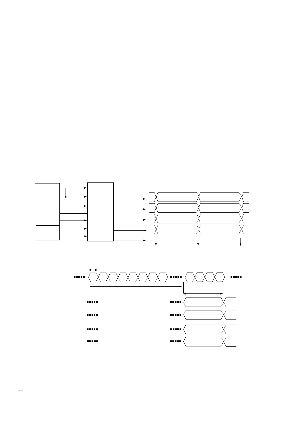
2626 Agere Systems Inc.
Preliminary Data Sheet
July 2001
1.0-1.25/2.0-2.5/3.125 Gbits/s Backplane Interface
ORCA ORT82G5 FPSC Eight-Channel
Backplane Transceiver Core Detailed
Description
(continued)
Receive Path (Backplane → FPGA)
The deMUX has to accumulate four sets of characters
presented to it at the SERDES receive interface and
put these out at one time at the low-speed receive
interface.
Another task of the deMUX is to recognize the synchronizing event and adjust the 4-byte boundary so that the
synchronizing character leads off a new 4-byte word.
This feature will be referred to as word alignment in
other areas of this document. Word alignment will only
occur when the communication channel is synchronized. When there is no synchronization of the link, the
deMUX will continue to output 4-byte words at some
arbitrary, but constant, boundary.
The deMUX passes on to the channel alignment FIFO
block a set of control signals that indicate the location
of the synchronizing event. RCOMMAx[3:0] are these
indicators. If there is no link synchronization, all of the
RCOMMAx[3:0] bits will be 0s independent of synchronizing events that come in. When the link is synchronized, then the bit that corresponds to the time of the
synchronization event will be set to a 1.
The relationship between a time sequence of values
input at SRBDx[7:0] to the values output at RWDx[31:0]
is shown in Figure 9 below. A parallel relationship
exists between SRBDx[8] and RWBIT8x[3:0] as well as
between SRBDx[9] and RWBIT9x[3:0].
2268(F)
Figure 9. Receive DeMUX Block for a Single SERDES Channel
8B/10B
ENCODER
PLL & CDR
1:4
DEMUX
(X 10)
XAUI LINK
SRBDx[9:0]
STATE
SBYTSYNCx
SRBC0x
SCVx
MACHINE
RWCKx
RCOMMAx[3:0]
RWBIT8x[3:0]
RWBIT9x[3:0]
SERDES DEMUX
SWDSYNCx
SRBC1x
pqrs txyz
SRBDx[7:0]
10-bit
RWDx[31:0]
p
7-0q7-0r7-0s7-0
t
7-0x7-0y7-0z7-0
p
8
s
8
q8r
8
t
8
z
8
x8y
8
p
9
s
9
q9r
9
t
9
z
9
x9y
9
p
c
s
c
qcr
c
t
c
z
c
xcy
c
p
q
r
s
t
x
y
z
40-bit
RWDx[31:24]
RWDx[23:16]
RWDx[15:8]
RWDx[7:0]
BLOCK
BLOCK
LATENCY = 4 RWCKx CLOCKS
Agere Systems Inc. 27
Preliminary Data Sheet
July 2001
1.0-1.25/2.0-2.5/3.1 25 Gbit s/s Backplane Interface
ORCA ORT82G5 FPSC Eight-Channel
Backplane Transceiver Core Detailed
Description
(continued)
5-8577 (F)
Figure 10. Interconnect of Streams for FIFO
Alignment
Multichann el Alignment (Backplane →
FPGA)
The alignment FIFO allows the transfer of all data to
the system clock. The FIFO sync block (Figure 10)
allows the system to be configured to allow the frame
alignment of multiple slightly varying data streams. This
optional alignment ensures that matching SERDES
streams will arrive at the FPGA end in perfect data
sync.
The ORT82G5 has a total of 8 channels (4 per SERDES). The incoming data of these channels can be
synchronized in several ways, or they can be independent of one other. For example, all four channels in a
SERDES can be aligned together to form a communication channel with a bandwidth of 10 Gbits/s as shown
in Figure 11.
Optionally, the alignment can be extended across SERDES to align all 8 channels in ORT82G5 as shown in
Figure 12. Individual channels within an alignment
group can be disabled (i.e., power down) without disrupting other channels.
Alternatively, two channels within a SERDES can be
aligned together; channel A and B and/or channel C
and D can form a pair as shown in Figure 1 3.
0673(F)
Figure 11. Example of SERDES A Alignment and
SERDES B Alignment
0674
Figure 12. Example of SERDES A and B Alignment
0675
Figure 13. Example of Multiple T win Channel
Alignment
SERDES A
STREAM A
SERDES A
STREAM B
SERDES A
STREAM C
SERDES A
STREAM D
SERDES B
STREAM A
SERDES B
STREAM B
SERDES B
STREAM C
FIFO
SYNC
SERDES B
STREAM D
SERDES A
SERDES B
SERDES A Stream A
ALL 4 ALIGNMENT OF SERDES A AND SERDES B
t
0
t
1
SERDES A Stream B
SERDES A Stream C
SERDES A Stream D
SERDES B Stream D
SERDES B Stream C
SERDES B Stream B
SERDES B Stream A
SERDES B Strea m D
SERDES B Strea m C
SERDES B Stream B
SERDES B Stream A
SERDES A Stream A
SERDES A Stream B
SERDES A Strea m C
SERDES A Strea m D
ALL 8 ALIGNMENT OF SERDES A AND SERDES B
t
0
SERDES A Stream A
SERDES A Stream B
SERDES A Stream C
SERDES A Stream D
SERDES B Stream D
SERDES B Stream C
SERDES B Stream B
SERDES B Stream A
SERDES A Stream A
SERDES A Stream B
SERDES A Stream C
SERDES A Stream D
SERDES B Stream D
SERDES B Stream C
SERDES B Stream B
SERDES B Stream A
TWO CHANNEL ALIGNMENT
t1t
2
SERDES A Stream A
SERDES A Stream B
SERDES A Stream C
SERDES A Strea m D
SERDES B Stream D
SERDES B Stream C
SERDES B Stream B
SERDES B Stream A
t
0
SERDES B Stream D
SERDES B Stream C
SERDES B Stream B
SERDES B Stream A
SERDES A Stream A
SERDES A Stream B
SERDES A Stream C
SERDES A Stream D
TWIN ALIGNMENT OF STREAM A & B OF SERDES A
TWIN ALIGNMENT OF STREAM C & D OF SERDES A
TWIN ALIGNMENT OF STREAM C & D OF SERDES B
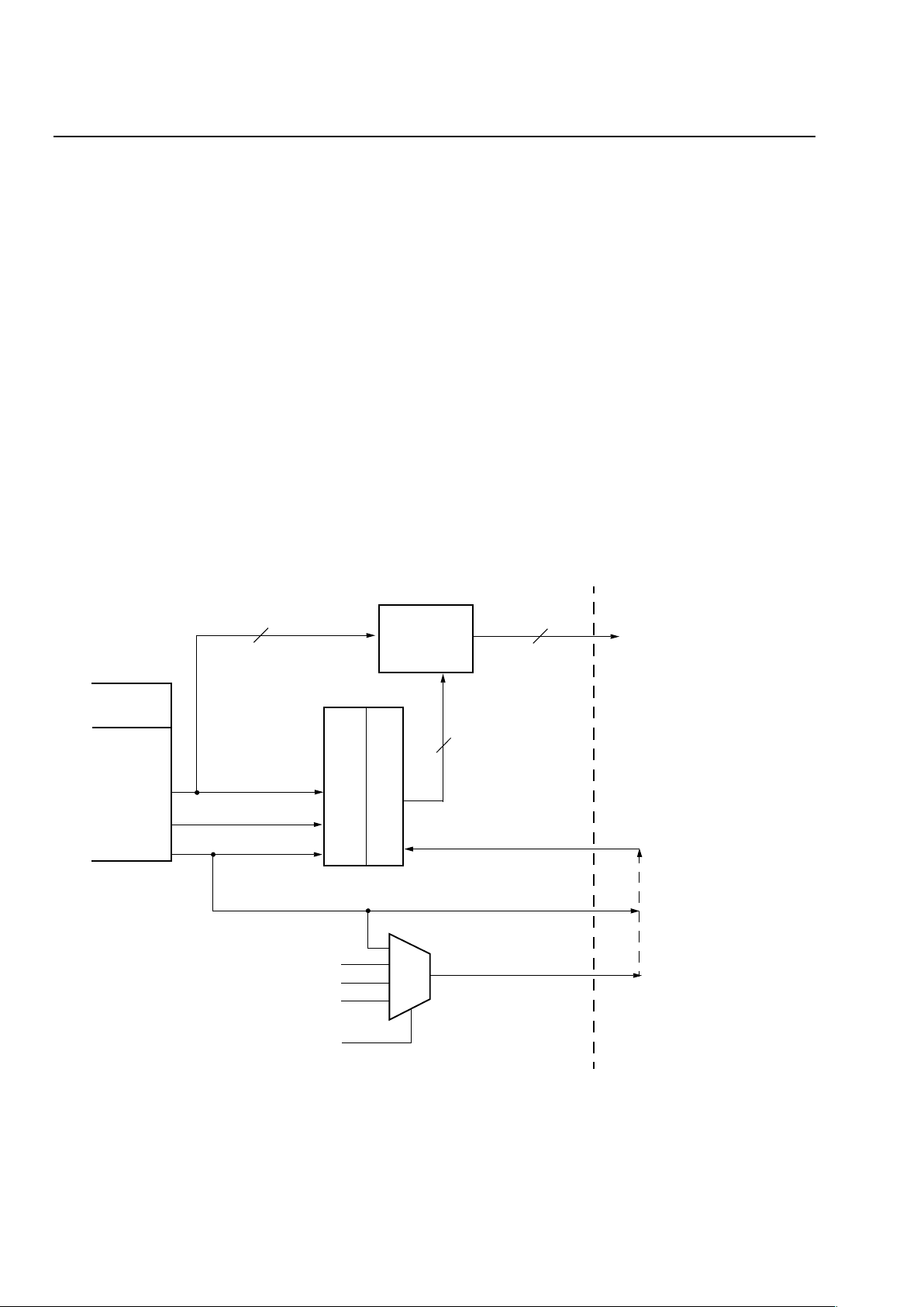
28 Agere Systems Inc.
Preliminary Data Sheet
July 2001
1.0-1.25/2.0-2.5/3.125 Gbits/s Backplane Interface
ORCA ORT82G5 FPSC Eight-Channel
Backplane Transceiver Core Detailed Description
(continued)
The multiplexed, receive word outputs to the FPGA are shown in Figure 14. These are each 40 bits wide. There are
eight of these interfaces, one for each data lane. Each consist of four 10-bit characters, or four decoded characters
(each 8 bits + 1 bit K_CTRL) + CH248_SYNCx status indicator bit depending on setting of NOCHALGNx control
register bits. Note that there is one control bit for a bank of channels, for a total of two control bits. Also, note that
while 10 bits are provided for each character when NOCHALGNx = 1, only the lower 9 bits of each character will be
meaningful if the 8B10BR bit is configured to 1 for that SERDES channel.
With x representing the bank (placeholder for A or B) and y representing the channel (placeholder for A, B, C , or D)
the 40-bit MRWDxy[39:0] is allocated as in Table x.
In the receive path, each channel is provided with a 24 word x 36-bit FIFO. The FIFO can perform two tasks: (1) to
change the clock domain from receive clock to a clock from the FPGA side, and (2) to align the receive data over 2,
4, or 8 channels. The input to the FIFO consists of 36-bit demultiplexed data, RWBYTESYNC[3:0], RWDx[31:0],
and RWBIT8x[3:0].
The four RWBYTESYNC bits are control signals, e.g., they can be the COMMADET signals indicating the presence
of COMMA character. The other 32 RWD bits are the 4 characters from the 8b/10b decoder. The RWBIT8 indicates
the presence of Km.n control character in the receive data byte. Only RWBIT8 and RWD inputs are stored in the
FIFO. During alignment process, RWBYTESYNC is used to synchronize multiple channels. If a channel is not in
any alignment group, it will set the FIFO-write-address to the beginning of the FIFO, and will set the FIFO-readaddress to the middle of the FIFO, at the first assertion of RWBYTESYNC after reset or after the resync command.
2269(F)
Figure 14. Multichannel Alignment FIFO Block for a Single SERDES Channel
1:4
DEMUX
(X 10)
XAUI LINK
STATE
MACHINE
RWCKx
RWBYTESYNC[3:0]
DEMUX
RWDx[31:0]
40
MRWDx
RWCKx
FPGA
MULTI-CHANNEL
ALIGNMENT
FIFO
2:1
MULTIPLEXER
(X 40)
40
36
CHANNEL ALIGN
EMBEDDED CORE
MUX
4 CHANNELS
RCKSEL[1:0]
RCK78(A,B)
RSYS_CLK(A,B)
(FROM GLOBAL OR
SECONDARY FPGA
CLOCK NETWORKS)
(TO LOCAL FPGA
SECONDARY CLOCK
NETWORK)
(TO GLOBAL FPGA
SYSTEM CLOCK
NETWORK)
 Loading...