

AGERE ORT4622BM432, ORT4622BC432, ORT4622BM432I, ORT4622BC432I Datasheet
Preliminary Data Sheet
March 2000
ORCA
®
ORT4622 Field-Programmable System Chip (FPSC)
Four-Channel x 622 Mbits/s Backplane Transceiver
Introduction
Lucent Technologies Microelectronics Group has
developed a solution for desi
g
ners who need the
man
y
advantages of FPGA-based design implemen-
tation, coupled with hi
g
h-speed serial backplane data
transfer. The 622 Mbits/s backplane transceiver
offers a clockless, hi
g
h-speed interface for interdevice communication on a board or across a backplane. The built-in clock recover
y
of the ORT4622
allows for hi
g
her system performance, easier-to-
desi
g
n clock domains in a multiboard system, and
fewer si
g
nals on the backplane. Network designers
will benefit from the backplane transceiver as a network termination device. The backplane transceiver
offers SONET scramblin
g
/descrambling of data and
streamlined SONET framin
g
, pointer moving, and
transport overhead handlin
g
, plus the programmable
lo
g
ic to terminate the network into proprietary systems. For non-SONET applications, all SONET functionalit
y
is hidden from the user and no prior
networkin
g
knowledge is required.
Embedded Core Features
■
Implemented in an
ORCA
Series 3 FPGA array.
■
Allows wide range of applications for SONET network termination application as well as generic data
moving for high-speed ba c k plane data transfer.
■
No knowledge of SONET /S D H needed in generic
applications. Simply supply data, 78 MHz clock, and
a frame pulse.
■
High-speed interface (H SI ) fu nc t ion for clock/data
recovery serial backplan e data transfer without
external clocks.
■
HSI function uses Lucent Technologies Microelectronics Group’s proven 622 Mbits/s serial interface
core.
■
Four-channel HSI function provides 622 Mbits/s
serial interface per channel for a total chip bandwidth of 2.5 Gbits/s (full duplex).
■
LVDS I/Os compliant with
EIA
*-644, support hot
insertion.
■
8:1 data multiplexing/d em ultiplexing for 77.76 MHz
byte-wide data processing in FPGA logic.
■
On-chip phase-lock loo p (PLL) clock meets B jitter
tolerance specification of ITU-T Recommendatio n
G.958 (0.6
UI
P-P
at 250 kHz).
■
Powerdown option of HSI rec eiver on a perchannel basis.
■
Highly efficient implementati on w it h only 3% overhead vs. 25% for 8B10B coding.
■
In-Band management and configuration.
■
Streamlined pointer proc essor (pointer mover) for
8 kHz frame alignment to system clocks.
■
Built-in boundry scan (
IEEE
†
1149.1 JTAG).
■
FIFOs align incoming data across all four channels
for STS-48 (2.5 Gbits/s) operation (in quad ST S-12
format).
■
1 + 1 protection supports ST S-12/STS-48 redundancy by either software or hardware control for
protection switching applications.
*
EIA
is a registered trademark of Electronic Industries Associa-
tion.
†
IEEE
is a registered trademark of The Institute of Electrical and
Electronics Engineers, Inc.
Table 1.
ORCA
ORT4622—Available FPGA Logic
‡The embedded core and interface are not included in the above gate counts. The usable gate count range f rom a logic-only gate count to
a gate count assuming 30% of the PFUs/SLICs being used as RAMs. The logic-only gate count includes each PFU/SLIC (counted as
108 gates per PFU/SLIC), including 12 gates pre-LUT/FF pair (eight per PFU), and 12 gates per SLC/FF pair (one per PFU). Each of the
four PIOs per PIC is counted as 16 gates (two FFs, fast-capture latch, output logic, CLK drivers, and I/O buffers). PFUs used as RAM are
counted at four gates per bit, with each PFU capable of implementing a 32 x 4 RAM (or 512 gates) per PFU.
Device
Usable
System
Gates
‡
Number of
LUTs
Number of
Registers
Max User
RAM
Max User
I/Os
Array Size
Number of
PFUs
ORT4622 60K—120K 4032 5304 64K 259 18 x 28 504

Table of Contents
Contents Page Contents Page
ORCA
ORT4622 FPSC Preliminary Data Sheet
Four-Channel x 622 Mbits/s Backplane Transceiver March 2000
Lucent Technologies 2
Introduction ...............................................................1
Embedded Core Features .........................................1
FPSC Highlights ........................................................ 4
Software Support ......................................................4
Description ................................................................ 5
What Is an FPSC? ..................................................5
FPSC Overview ......................................................5
FPSC Gate Counting ..............................................5
FPGA/Embedded Core Interface ............................5
ORCA
Foundry Development System ....................5
FPSC Design Kit .....................................................6
FPGA Logic Overview ............................................6
PLC Logic ................. ..............................................6
PIC Logic ................................................................7
System Features ....................................................7
Routing ................................................................... 7
Configuration .......................................................... 7
More Series 3 Information ......................................7
ORT4622 Overview ...................................................8
Device Layout .........................................................8
Backplane Transceiver Interface ............................8
HSI Interface ...........................................................10
STM Macrocell ........................................................10
CPU Interface .........................................................10
FPGA Interface .......................................................10
FPSC Configuration ................................................12
Generic Backplane Transceiver Application .......... ....13
Backplane Transceiver Core Detailed Description .... 13
HSI Macro ...............................................................13
STM Transmitter (FPGA -> Backplane) ..................15
STM Receiver (Backplane -> FPGA) ......................19
Powerdown Mode ...................................................25
Redundancy and Protection Switching ...................25
Memory Map .................................. .................... ....... 26
Definition of Register Types ...................................26
Memory Map Overview ...........................................27
Powerup Sequencing for ORT4622 Device .............. 35
FPGA Configuration Data Format ............................. 36
Using
ORCA
Foundry to Generate Conf iguration
RAM Data ............................................................36
FPGA Configuration Data Frame ...........................36
Bit Stream Error Checking .........................................38
FPGA Configuration Modes ......................................38
Absolute Maximum Ratings .......................................39
Recommend Operating Conditions ...........................39
Electrical Characteristics ...........................................40
HSI Circuit Specifications ..........................................41
Input Data ...............................................................41
Jitter Tolerance .......................................................41
Generated Output Jitter ..........................................41
PLL ......................................................................... 41
Input Reference Clock ............................................41
HSI Circuit Specifications ..........................................41
Power Supply Decoupling LC Circuit ......................42
LVDS I/O ...................................................................43
LVDS Receiver Buffer Requirements .....................44
Timing Characteristics ...............................................45
Description .............................................................. 45
PFU Timing .............................................................46
PLC Timing .......... ...................................................46
SLIC Timing ............................................................46
PIO Timing ..................... ........................................ .46
Special Function Timing .......... ...............................46
Clock Timing ...........................................................46
Configuration Timing ...............................................46
Readback Timing ....................................................46
Input/Output Buffer Me as urement Conditions
(on-LVDS Buffer) ......................................................56
FPGA Output Buffer Characteristics .........................57
LVDS Buffer Characteristics ......................................58
Termination Resistor ...............................................58
LVDS Driver Buffer Capabilities ..............................58
Estimating Power Dissipation ....................................59
ORT4622 Clock Power ...........................................59
Pin Information ..........................................................60
Package Thermal Characteristics Summary .............83
Θ
JA ......................................................................... 83
ψ
JC ......................................................................... 83
Θ
JC ......................................................................... 83
Θ
JB ......................................................................... 83
FPGA Maximum Junction Temperature .................83
Package Thermal Characteristics .............................84
Package Coplanarity ......................................... ........84
Package Parasitics ....................................................84
Package Outline Diagrams ...................... ..................86
Terms and Definitions .............................................86
432-Pin EBGA ........................................................87
680-Pin PBGAM .....................................................88
Ordering Information .................................................90
List of Figures
Figure 1.
ORCA
ORT4622 Block Diagram.................8
Figure 2. Architecture of ORT4622 Backplane
Transceiver..............................................................11
Figure 3. HSI Functional Block Diagram ....................14
Figure 4. Byte Ordering of In put/Output Interface in
STS-12 Mode......................... ..................................15
Figure 5. Interconnect of Streams for FIFO................20
Figure 6. Alignment of Four STS-12 Streams ............20
Figure 7. Examples of Link Alignment........................21
Figure 8. Pointer Mover State Machine......................22
Figure 9. SPE and C1J1 Functionality .......................24
Figure 10. SPE Stuff Bytes.........................................25
Figure 11. Serial Configuration Data Format—
Autoincrement Mode................................................37

Lucent Technologies Inc. 3
Preliminary Data Sheet
ORCA
ORT4622 FPSC
March 2000 Four-Channel x 622 Mbits/s Backplane Transceiver
Table of Contents
(continued)
Figure Page Table Page
Figure 12. Serial Config uration Data Format—
Explicit Mode.......................... ..................................37
Figure 13. Sample Pow er Supply Filter Network for
Analog HSI Power Supply Pins................................42
Figure 14. Transmit Parallel Port Timing
(Backplane -> FPGA)...............................................48
Figure 15. Transmit Transport Delay
(FPGA -> Backplane).................................... ...........49
Figure 16. Receive Parallel Port Timing
(Backplane -> FPGA)...............................................50
Figure 17. Protection Switch Timing...........................51
Figure 18. TOH Input Serial Por t Timing
(FPGA -> Backplane).................................... ...........52
Figure 19. TOH Output Serial Po rt Timing
(Backplane -> FPGA)...............................................53
Figure 20. CPU Write Transaction..............................54
Figure 21. CPU Read Transaction..............................55
Figure 22. ac Test Loads ............................................56
Figure 23. Output Buffer Delays.................................5 6
Figure 24. Input Buffer Delays....................................56
Figure 25. Sinklim (T
J
= 25 °C, VDD = 3.3 V)..............57
Figure 26. Slewlim (T
J
= 25 °C, VDD = 3.3 V)............. 5 7
Figure 27. Fast (T
J
= 25 °C, VDD = 3.3 V) ..................57
Figure 28. Sinklim (T
J
= 125 °C, VDD = 3.0 V)............57
Figure 29. Slewlim (T
J
= 125 °C, VDD = 3.0 V)...........57
Figure 30. Fast (T
J
= 125 °C, VDD = 3.0 V)................57
Figure 31. LVDS Driver and Receiver and
Associated Internal Components.............................58
Figure 32. LVDS Driver and Receiver.........................58
Figure 33. LVDS Driver...............................................58
Figure 34. Package Parasitics....................................85
List of Tables
Table 1.
ORCA
ORT4622—Available
FPGA Logic..............................................................1
Table 2. ORT4622 Array ............................................9
Table 3. Transmitter TOH on LVDS Output
(Transparent Mode)..................................................17
Table 4. Transmitter TOH on LVDS Output
(TOH Insert Mode)...................................................17
Table 5. Valid Starting Positions for an STS-Mc ........ 2 1
Table 6. Receiver TOH (Output Parallel Bus).............23
Table 7. SPE and C1J1 Functionality ........................24
Table 8. Structural Register Elements ........... ...........26
Table 9. Memory Map ...............................................27
Table 10. Memory Map Bit Descriptions....................31
Table 11. Configuration Frame Format and
Contents...................................................................37
Table 12. Configuration Modes..................................38
Table 13. Absolute Maximum Ratings........................39
Table 14. Recommend Operating Conditions ............39
Table 15. General Electrical Characteristics ..............39
Table 16. Electrical Charac t eristics for FPGA I/O.......40
Table 17. Electrical Charac t eristics for Embedded
Core I/O Other than LVDS I/O..................................40
Table 18. Jitter Tolerance ...........................................41
Table 19. PLL.............................................................41
Table 20. Input Reference Clock ................................41
Table 21. LVDS Driver dc Data ..................................43
Table 22. LVDS Driver ac Data ..................................43
Table 23. LVDS Receiver dc Data .............................44
Table 24. LVDS Receiver ac Data .............................44
Table 25. LVDS Receiver Power Consumption ..........44
Table 26. LVDS Operating Parameters.......................44
Table 27. Derating for Commercial Devices
(I/O Supply
V
DD
).......................................................45
Table 28. Derating for Commercial Devices
(I/O Supply
V
DD
2).....................................................45
Table 29. ORT4622 Embedded Core and FP GA
Interface Clock Operation Frequencies....................46
Table 30. Timing Requirements (Transmit
Parallel Port Timing) ................................................48
Table 31. Timing Requirements
(Transmit Transport Delay) .......................................49
Table 32. Timing Requirements
(Receive Parallel Port Timing) .................................50
Table 33. Timing Requirements
(Protection Switch Timing) ......................................51
Table 34. Timing Requirements
(TOH Input Serial Port Timing) ................................52
Table 35. Timing Requirements
(TOH Output Serial Port Timing) .............................53
Table 36. Timing Requirements
(CPU Write Transaction) ..................................... .....54
Table 37. Timing Requirements
(CPU Read Transaction) ....................... ...................55
Table 38. Embedded Block Power Dissipation...........59
Table 39. FPGA Common-Function
Pin Description.........................................................60
Table 40. FPSC Function Pin Description ...............63
Table 41. Embedded Core/ F PGA Interface
Signal Description ...................................................65
Table 42. Embedded Core/ F PGA Interface
Signal Locations ....................................................67
Table 43. 432-Pin EBGA Pinout.................................68
Table 44. 680-Pin PBGAM Pinout .............................74
Table 45.
ORCA
ORT4622 Plastic Package
Thermal Guidelines..................................................83
Table 46.
ORCA
ORT4622 Package Parasitics..........84
Table 47. Voltage Options ..........................................89
Table 48. Temperature Options..................................89
Table 49. Pa ckage Type Options................................90
Table 50.
ORCA
Series 3+ Package Matrix...............90

ORCA
ORT4622 FPSC
Preliminary Data Sheet
Four-Channel x 622 Mbits/s Backplane Transceiver March 2000
4 Lucent Technologies Inc.
Lucent Technologies Inc.
Embedded Core Features
(continued)
■
Pseudo-SONET protocol including A1/A2 framing.
■
SONET scrambling and descrambling for required
ones density (optional).
■
Selected transport overhead (TOH) bytes insertion
and extraction for interdevice communication via the
TOH serial link.
FPSC Highlights
■
Implemented as an embedded core in the
ORCA
Series 3+ FPSC architecture.
■
Allows the user to integrate the core with up to 120K
gates of programmable logic (all in one device) and
provides up to 242 user I/Os in addition to the
embedded core I/O pins.
■
FPGA portion retains all of the features of the
ORCA
Series 3 FPGA architecture:
— High-performance, cost-effective, 0.25 µm, 5-level
metal technology.
— Twin-quad programmable function unit (PFU)
architecture with eight 16-bit look-up tables
(LUTs) per PFU, organized in two nibbles for use
in nibble- or byte-wide functions. Allows for mixed
arithmetic and logic functions in a single PFU.
— Softwired LUTs (SWL) allow fast cascading of up
to three levels of LUT logic in a single PFU.
— Supplemental logic and interconnect cell (SLIC)
provides 3-statable buffers, up to 10-bit decoder,
and
PAL
*-like AND-OR-INVERT (AOI) in each
programmable logic cell (PLC).
— Up to three ExpressCLK inputs allow extremely
fast clocking of signals on- and off-chip plus
access to internal general clock routing.
— Dual-use microprocessor interface (MPI) can be
used for configuration, as well as for a generalpurpose interface to the FPGA. Glueless interface
to
i960
†
and
PowerPC
‡
processors with user-
configurable address space provided.
— Programmable clock manager (PCM) adjusts
clock phase and duty cycle for input clock rates
from 5 MHz to 120 MHz. The PCM may be com-
bined with FPGA logic to create complex
functions, such as digital phas e-l ocked loops,
frequency counters, and frequenc y sy nth es izers
or clock doublers. Two PCMs are provided per
device.
— True internal 3-state, bidirectional buses with
simple control provided by the SLIC.
— 32 x 4 RAM per PFU, configurable as single or
dual port. Create large, fast RAM/ROM blocks
(128 x 8 in only eight PFUs) using the SLIC
decoders as bank drivers.
— Built -in bound ary scan (
IEEE
1149.1 JTAG) and
TS_ALL testability function to 3-state all I/O pins.
■
High-speed, on-chip interface provided between
FPGA logic and embedded core to reduce bottlenecks typically found when interfacing off-chip.
Software Support
■
Supported by
ORCA
Foundry software and third-
party CAE tools for implementing
ORCA
Series 3+
devices and simulation/timing analysis with the
embedded core functions.
■
Embedded core configuration options and simulation
netlists generated by FPSC Configuration Manager
utility.
*
PAL
is a trademark of Advanced Micro Devices, Inc.
†
i960
is a registered trademark of Intel Corporation.
‡
PowerPC
is a registered trademark of International Business
Machines Corporation.

Lucent Technologies Inc. 5
Preliminary Data Sheet
ORCA
ORT4622 FPSC
March 2000 Four-Channel x 622 Mbits/s Backplane Transceiver
Lucent Technologies Inc.
Description
What Is an FPSC?
FPSCs, or field-programmable system chips, are
devices that combine field-programmable logic with
ASIC or mask-programmed logic on a single device.
FPSCs provide the time to market and flexibility of
FPGAs, the design effort savings of using soft intellectual property (IP) cores, and the speed, design density,
and economy of ASICs.
FPSC Overview
Lucent’s Series 3+ FPSCs are created from Series 3
ORCA
FPGAs. To create a Series 3+ FPSC, several
rows of programmable logic cells (see FPGA Logic
Overview section for FPGA logic details) are removed
from a Series 3
ORCA
FPGA, and the area is replaced
with an embedded logic core. Other than replacing
some FPGA gates with ASIC gates, at greater than
10:1 efficiency, none of the FPGA functionality is
changed—all of the Series 3 FPGA capability is
retained: MPI, PCMs, boundary scan, etc. The rows of
programmable logic are replaced at the bottom of the
device, allowing pins on the bottom and sides of the
replaced rows to be used as I/O pins for the embedded
core. The remainder of the device pins retain their
FPGA functionality as do special function FPGA pins
within the embedded core area.
The embedded cores can take many forms and generally come from Lucent Technologies ASIC libraries.
Other offerings allow customers to supply their own
core functions for the creation of custom FPSCs.
FPSC Gate Counting
The total gate count for an FPSC is the sum of its
embedded core (standard-cell/ASIC gates) and its
FPGA gates. Because FPGA gates are generally
expressed as a usable range with a nominal value, the
total FPSC gate count is sometimes expressed in the
same manner. Standard-cell ASIC gates are, however,
10 to 25 times more silicon area efficient than FPGA
gates. Therefore, an FPSC with an embedded function
is gate equivalent to an FPGA with a much larger gate
count.
FPGA/Embedded Core Interface
The interface between the FPGA logic and the embedded core is designed to look like FPGA I/Os from the
FPGA side, simplifying interface signal routing and providing a unified approach with general FPGA design.
Effectively, the FPGA is designed as if signals were
going off of the device to the embedded core, but the
on-chip interface is much faster than going off-chip and
requires less power. All of the delays for the interface
are precharacterized and accounted for in the
ORCA
Foundry Development System.
Clock spines also can pass across the FPGA/embed-
ded core boundary. This allows for fast, low-skew
clocking between the FPGA and the embedded core.
Many of the special signals from the FPGA, such as
DONE and global set/reset, are also available to the
embedded core, making it possible to fully integrate the
embedded core with the FPGA as a system.
For even greater system flexibility, FPGA configuration
RAMs are available for use by the embedded core.
This allows for user-programmable options in the
embedded core, in turn allowing for greater flexibility.
Multiple embedded core configurations may be
designed into a single device with user-programmable
control over which configurations are implemented, as
well as the capability to change core functionality simply by reconfiguring the device.
ORCA
Foundry Development System
The
ORCA
Foundry Development System is used to
process a design from a netlist to a configured FPSC.
This system is used to map a design onto the
ORCA
architecture and then place and route it using
ORCA
Foundry’s timing-driven tools. The development system
also includes interfaces to, and libraries for, other popular CAE tools for design entry, synthesis, simulation,
and timing analysis.
The
ORCA
Foundry
Development System interfaces to
front-end design entry tools and provides the tools to
produce a configured FPSC. In the design flow, the
user defines the functionality of the FPGA portion of
the FPSC and embedded core settings at two points in
the design flow: at design entry and at the bit stream
generation stage. Following design entry, the development system’s map, place, and route tools translate the
netlist into a routed FPSC. A static timing analysis tool
is provided to determine device speed, and a backannotated netlist can be created to allow simulation.

ORCA
ORT4622 FPSC
Preliminary Data Sheet
Four-Channel x 622 Mbits/s Backplane Transceiver March 2000
6 Lucent Technologies Inc.
Lucent Technologies Inc.
Description
(continued)
Timing and simulation output files from
ORCA
Foundry
are also compatible with many third-party analysis
tools. Its bit stream generator is then used to generate
the configuration data which is loaded into the FPSC’s
internal configuration RAM.
When using the bit stream generator, the user selects
options that affect the functionality of the FPSC. Combined with the front-end tools,
ORCA
Foundry
produces configuration data that implements the various
logic and routing options discussed in this data sheet.
FPSC Design Kit
Development is facilitated by an FPSC design kit
which, together with
ORCA
Foundry and third-party
synthesis and simulation engines, provides all software
and documentation required to design and verify an
FPSC implementation. Included in the kit are the FPSC
configuration manager, HDL gate-level structural
netlists, all necessary synthesis libraries, and complete
online documentation. The kit's software couples with
ORCA
Foundry, providing a seamless FPSC design
environment. More information can be obtained by visiting the
ORCA
website or contacting a local sales
office, both listed on the last page of this document.
FPGA Logic Overview
ORCA
Series 3 FPGA logic is a new generation of
SRAM-based FPGA logic built on the successful
Series 2 FPGA li ne from Lucent Technologies Microelectronics Group, with enhancements and innovations
geared toward today’s high-speed designs on a single
chip. Designed from the start to be synthesis friendly
and to reduce place and route times while maintaining
the complete routability of the
ORCA
Series 2 devices,
the Series 3 more than doubles the logic available in
each logic block and incorporates system-level f eatures
that can further reduce logic requirements and
increase system speed.
ORCA
Series 3 devices contain many new patented enhancements and are offered
in a variety of packages, speed grades, and temperature ranges.
ORCA
Series 3 FPGA logic consists of three basic elements: programmable logic cells (PLCs), programmable input/output cells (PICs), and system-level features.
An array of PLCs is surrounded by PICs. Each PLC
contains a programmable function unit (PFU), a supplemental logic and interconnect cell (SLIC), local routing resources, and configuration RAM. Most of the
FPGA logic is performed in the PFU, but decoders,
PAL
-like functions, and 3-state buffering can be performed in the SLIC. The PICs provide device inputs
and outputs and can be used to register signals and to
perform input demultiplexing, output multiplexing, and
other functions on two output signals. Some of the system-level functions include the new microprocessor
interface (
MPI
) and the programmable clock manager
(
PCM
).
PLC Logic
Each PFU within a PLC contains eight 4-input (16-bit)
look-up tables (LUTs), eight latches/flip-flops (FFs),
and one additional flip-flop that may be used independently or with arithmetic functions.
The PFU is organized in a twin-quad fashion: two sets
of four LUTs and FFs that can be controlled independently. LUTs may also be combined for use in arithmetic functions using fast-carry chain logic in either
4-bit or 8-bit modes. The carry-out of either mode may
be registered in the ninth FF for pipelining. Each PFU
may also be configured as a synchronous 32 x 4
single- or dual-port RAM or ROM. The FFs (or latches)
may obtain input from LUT outputs or directly from
invertible PFU inputs, or they can be tied high or tied
low. The FFs also have programmable clock polarity,
clock enables, and local set/reset.
The SLIC is connected to PLC routing resources and to
the outputs of the PFU. It contains 3-state, bidirectional
buffers and logic to perform up to a 10-bit AND function
for decoding, or an AND-OR with optional INVERT
(AOI) to perform
PAL
-like functions. The 3-state drivers
in the SLIC and their direct connections to the PFU outputs make fast, true 3-state buses possible within the
FPGA logic, reducing required routing and allowing for
real-world system performa nce.

Lucent Technologies Inc. 7
Preliminary Data Sheet
ORCA
ORT4622 FPSC
March 2000 Four-Channel x 622 Mbits/s Backplane Transceiver
Lucent Technologies Inc.
Description
(continued)
PIC Logic
The Series 3 PIC addresses the demand for everincreasing system clock speeds. Each PIC contains
four programmable inputs/outputs (PIOs) and routing
resources. On the input side, each PIO contains a fastcapture latch that is clocked by an
ExpressCLK
. This
latch is followed by a latch/FF that is clocked by a system clock from the internal general clock routing. The
combination provides for very low setup requirements
and zero hold times for signals coming on-chip. It may
also be used to demultiplex an input signal, such as a
multiplexed address/data signal, and register the signals without explicitly building a demultiplexer. Two
input signals are available to the PLC array from each
PIO, and the
ORCA
Series 2 capability to use any input
pin as a clock or other global input is maintained.
On the output side of each PIO, two outputs from the
PLC array can be routed to each output flip-flop, and
logic can be associated with each I/O pad. The output
logic associated with each pad allows for multiplexing
of output signals and other functions of two output signals.
The output FF, in combination with output signal multiplexing, is particularly useful for registering address
signals to be multiplexed with data, allowing a full clock
cycle for the data to propagate to the output. The I/O
buffer associated with each pad is the same as the
ORCA
Series 3 buffer.
System Features
The Series 3 also provides system-level functionality
by means of its dual-use microprocessor interface
(MPI) and its innovative programmable clock manager
(PCM). These functional blocks allow for easy glueless
system interfacing and the capability to adjust to varying conditions in today’s high-speed systems. Since
these and all other Series 3 features are available in
every Series 3+ FPSC, they can also interface to the
embedded core providing for easier system integration.
Routing
The abundant routing resources of
ORCA
Series 3
FPGA logic are organized to route signals individually
or as buses with related control signals. Clocks are
routed on a low-skew, high-speed distribution network
and may be sourced from PLC logic, externally from
any I/O pad, or from the very fast
ExpressCLK
pins.
ExpressCLKs may be glitchlessly and independently
enabled and disabled with a programmable control signal using the
StopCLK
feature. The improved PIC routing resources are now similar to the patented intra-PLC
routing resources and provide great flexibility in moving
signals to and from the PIOs. This flexibility translates
into an improved capability to route designs at the
required speeds when the I/O signals have been
locked to specific pins.
Configuration
The FPGA logic’s functionality is determined by internal configuration RAM. The FPGA logic’s internal initialization/configuration circuitry loads the configuration
data at powerup or under system control. The RAM is
loaded by using one of several configuration modes,
including serial EEPROM, the microprocessor interface, or the embedded function core.
More Series 3 Information
For more information on Series 3 FPGAs, please refer
to the Series 3 FPGA data sheet, available on the
ORCA
worldwide website or by contacting Lucent
Technologies as directed on the back of this data
sheet.
88 Lucent Technologies Inc.
ORCA
ORT4622 FPSC Preliminary Data Sheet
Four-Channel x 622 Mbits/s Backplane Transceiver March 2000
Lucent Technologies Inc.
ORT4622 Overview
Device Layout
The ORT4622 FPSC provides a high-speed backplane
transceiver combined with FPGA logic. The device is
based on a 2.5 V 3.3 V I/O OR3L125B FPGA. The
OR3L125B has a 28 x 28 array of programmable logic
cells (PLCs). For the ORT4622, the bottom ten rows of
PLCs in the array were replaced with the embedded
backplane transceiver core. The ORT4622 embedded
core comprises the HSI macrocell, the synchronous
transport module (STM) macrocell, a CPU interface,
and LVDS I/Os. The four full-duplex channels perform
data transfer, scrambling/descrambling and framing at
the rate of 622 Mbits/s. Figure 1 shows the ORT4622
block diagram.
Table 2
shows a schematic view of the ORT4622. The
upper portion of the device is an 18 x 28 array of PLCs
surrounded on the left, top, and right by programmable
input/output cells (PICs). At the bottom of the PLC
array are the core interface cells (CICs) connecting to
the embedded core region. The embedded core region
contains the backplane transceiver functionality of the
device. It is surrounded on the left, bottom, and right by
backplane transceiver dedicated I/Os as well as power
and special function FPGA pins. Also shown are the
interquad routing blocks (hIQ, vIQ) present in the
Series 3 FPGA devices. System-level functions
(located in the corners of the PLC array), routing
resources, and configuration RAM are not shown in
Table 2
.
Backplane Transceiver Interface
The advantage of the ORT4622 FPSC is to bring specific networking functions to an early market presence
with programmable logic in FPGA syst em.
The 622 Mbits/s backplane transceiver core allows the
ORT4622 to communicate across a backplane or on a
given board at an aggregate speed of 2.5 Gbits/s, providing a physical medium for high-speed asynchronous
serial data transfer between system devices. This
device is intended for, but not limited to, connecting terminal equipment in SONET/SDH and ATM systems.
For networking applications, the ORT4622 offers a
pseudo SONET framer and scrambler/descrambler
interface capable of frame synchronization and insertion/extraction of selectable transport overhead bytes
and SONET scrambling and descrambling for four
STS-12 (622 Mbits/s) channels. The channels are synchronized to each other by a user-provided 8 kHz
frame pulse. The ORT4622 also provides STS-48
(2.5 Gbits/s) operation across all four channels where
each channel is in STS-12 format. The pseudo-SONET
framer of OR4622 is designed with a reduced set of the
SONET framing algorithm. The pointer processing
capability is more suitable for low error rate intersystem
data communication, particular for backplane transceiver applications. Figure 2 shows the architecture of
the ORT4622 backplane transceiver core.
5-8113(F)
Figure 1.
ORCA
ORT4622 Block Diagram
• CLOCK/DATA
RECOVERY
4 FULL-
DUPLEX
SERIAL
CHANNELS
BYTE-
WIDE
DATA
FPGA LOGIC
STANDARD
FPGA
I/Os
LVDS
622 Mbits/s
DATA
622 Mbits/s
DATA
STM
• POINTER MOVER
• SCRAMBLING
• FIFO ALIGNMENT
• TOH PROCESSOR
I/Os
HSI
4
4

Lucent Technologies Inc. 9
Preliminary Data Sheet
ORCA
ORT4622 FPSC
March 2000 Four-Channel x 622 Mbits/s Backplane Transceiver
Lucent Technologies Inc.
ORT4622 Overview
(continued)
Table 2
. ORT4622 Array
IIII IIII IIII IIII IIII IIII IIII IIII IIII IIII IIII IIII IIII IIII IIII IIII IIII IIII IIII IIII IIII IIII IIII IIII IIII IIII IIII IIII
PT1 PT2 PT3 PT4 PT5 PT6 PT7 PT8 PT9 PT10 PT11 PT12 PT13 PT14 PT15 PT16 PT17 PT18 PT19 PT20 PT21 PT22 PT23 PT24 PT25 PT26 PT27 PT28
IIII
PL1
R1C1R1C2R1C3R1C4R1C5R1C6R1C7R1C8R1C9R1
C10R1C11R1C12R1C13R1C14R1C15R1C16R1C17R1C18R1C19R1C20R1C21R1C22R1C23R1C24R1C25R1C26R1C27R1C28
PR1
IIII
IIII
PL2
R2C1R2C2R2C3R2C4R2C5R2C6R2C7R2C8R2C9R2
C10R2C11R2C12R2C13R2C14R2C15R2C16R2C17R2C18R2C19R2C20R2C21R2C22R2C23R2C24R2C25R2C26R2C27R2C28
PR2
IIII
IIII
PL3
R3C1R3C2R3C3R3C4R3C5R3C6R3C7R3C8R3C9R3
C10R3C11R3C12R3C13R3C14R3C15R3C16R3C17R3C18R3C19R3C20R3C21R3C22R3C23R3C24R3C25R3C26R3C27R3C28
PR3
IIII
IIII
PL4
R4C1R4C2R4C3R4C4R4C5R4C6R4C7R4C8R4C9R4
C10R4C11R4C12R4C13R4C14R4C15R4C16R4C17R4C18R4C19R4C20R4C21R4C22R4C23R4C24R4C25R4C26R4C27R4C28
PR4
IIII
IIII
PL5
R5C1R5C2R5C3R5C4R5C5R5C6R5C7R5C8R5C9R5
C10R5C11R5C12R5C13R5C14R5C15R5C16R5C17R5C18R5C19R5C20R5C21R5C22R5C23R5C24R5C25R5C26R5C27R5C28
PR5
IIII
IIII
PL6
R6C1R6C2R6C3R6C4R6C5R6C6R6C7R6C8R6C9R6
C10R6C11R6C12R6C13R6C14R6C15R6C16R6C17R6C18R6C19R6C20R6C21R6C22R6C23R6C24R6C25R6C26R6C27R6C28
PR6
IIII
IIII
PL7
R7C1R7C2R7C3R7C4R7C5R7C6R7C7R7C8R7C9R7
C10R7C11R7C12R7C13R7C14R7C15R7C16R7C17R7C18R7C19R7C20R7C21R7C22R7C23R7C24R7C25R7C26R7C27R7C28
PR7
IIII
IIII
PL8
R8C1R8C2R8C3R8C4R8C5R8C6R8C7R8C8R8C9R8
C10R8C11R8C12R8C13R8C14R8C15R8C16R8C17R8C18R8C19R8C20R8C21R8C22R8C23R8C24R8C25R8C26R8C27R8C28
PR8
IIII
IIII
PL9
R9C1R9C2R9C3R9C4R9C5R9C6R9C7R9C8R9C9R9
C10R9C11R9C12R9C13R9C14R9C15R9C16R9C17R9C18R9C19R9C20R9C21R9C22R9C23R9C24R9C25R9C26R9C27R9C28
PR9
IIII
IIII
PL10
R10C1R10C2R10C3R10C4R10C5R10C6R10C7R10C8R10C9R10
C10
R10
C11
R10
C12
R10
C13
R10
C14
R10
C15
R10
C16
R10
C17
R10
C18
R10
C19
R10
C20
R10
C21
R10
C22
R10
C23
R10
C24
R10
C25
R10
C26
R10
C27
R10
C28
PR10
IIII
IIII
PL11
R11C1R11C2R11C3R11C4R11C5R11C6R11C7R11C8R11C9R11
C10
R11
C11
R11
C12
R11
C13
R11
C14
R11
C15
R11
C16
R11
C17
R11
C18
R11
C19
R11
C20
R11
C21
R11
C22
R11
C23
R11
C24
R11
C25
R11
C26
R11
C27
R11
C28
PR11
IIII
IIII
PL12
R12C1R12C2R12C3R12C4R12C5R12C6R12C7R12C8R12C9R12
C10
R12
C11
R12
C12
R12
C13
R12
C14
R12
C15
R12
C16
R12
C17
R12
C18
R12
C19
R12
C20
R12
C21
R12
C22
R12
C23
R12
C24
R12
C25
R12
C26
R12
C27
R12
C28
PR12
IIII
IIII
PL13
R13C1R13C2R13C3R13C4R13C5R13C6R13C7R13C8R13C9R13
C10
R13
C11
R13
C12
R13
C13
R13
C14
R13
C15
R13
C16
R13
C17
R13
C18
R13
C19
R13
C20
R13
C21
R13
C22
R13
C23
R13
C24
R13
C25
R13
C26
R13
C27
R13
C28
PR13
IIII
IIII
PL14
R14C1R14C2R14C3R14C4R14C5R14C6R14C7R14C8R14C9R14
C10
R14
C11
R14
C12
R14
C13
R14
C14
R14
C15
R14
C16
R14
C17
R14
C18
R14
C19
R14
C20
R14
C21
R14
C22
R14
C23
R14
C24
R14
C25
R14
C26
R14
C27
R14
C28
PR14
IIII
IIII
PL15
R15C1R15C2R15C3R15C4R15C5R15C6R15C7R15C8R15C9R15
C10
R15
C11
R15
C12
R15
C13
R15
C14
R15
C15
R15
C16
R15
C17
R15
C18
R15
C19
R15
C20
R15
C21
R15
C22
R15
C23
R15
C24
R15
C25
R15
C26
R15
C27
R15
C28
PR15
IIII
IIII
PL16
R16C1R16C2R16C3R16C4R16C5R16C6R16C7R16C8R16C9R16
C10
R16
C11
R16
C12
R16
C13
R16
C14
R16
C15
R16
C16
R16
C17
R16
C18
R16
C19
R16
C20
R16
C21
R16
C22
R16
C23
R16
C24
R16
C25
R16
C26
R16
C27
R16
C28
PR16
IIII
IIII
PL17
R17C1R17C2R17C3R17C4R17C5R17C6R17C7R17C8R17C9R17
C10
R17
C11
R17
C12
R17
C13
R17
C14
R17
C15
R17
C16
R17
C17
R17
C18
R17
C19
R17
C20
R17
C21
R17
C22
R17
C23
R17
C24
R17
C25
R17
C26
R17
C27
R17
C28
PR17
IIII
IIII
PL18
R18C1R18C2R18C3R18C4R18C5R18C6R18C7R18C8R18C9R18
C10
R18
C11
R18
C12
R18
C13
R18
C14
R18
C15
R18
C16
R18
C17
R18
C18
R18
C19
R18
C20
R18
C21
R18
C22
R18
C23
R18
C24
R18
C25
R18
C26
R18
C27
R18
C28
PR18
IIII
II
ASB1 ASB2 ASB3 ASB4 ASB5 ASB6 ASB7 ASB8 ASB9 ASB10 ASB11 ASB12 ASB13 ASB14 ASB15 ASB16 ASB17 ASB18 ASB19 ASB20 ASB21 ASB22 ASB23 ASB24 ASB25 ASB26 ASB27 ASB28
II
II
EMBEDDED CORE AREA
II
IIII
IIII
IIII
IIII
IIII
IIII
IIII
IIII
IIII
IIII
IIII
IIII
IIII
IIII
IIII
IIII
IIII
IIII
IIII IIII IIII IIII IIII IIII IIII IIII IIII IIII IIII IIII IIII IIII IIII IIII IIII IIII IIII IIII IIII IIII IIII IIII IIII IIII IIII IIII

ORCA
ORT4622 FPSC
Preliminary Data Sheet
Four-Channel x 622 Mbits/s Backplane Transceiver March 2000
10 Lucent Technologies Inc.
Lucent Technologies Inc.
ORT4622 Overview
(continued)
HSI Interface
The high-speed interconnect (HSI) macrocell is used
for clock/data recovery and MUX/deMUX between
77.76 MHz byte-wide internal data buses and
622 Mbits/s external serial links.
The HSI interface receives four 622 Mbits/s serial input
data streams from the LVDS inputs and provides four
independent 77.76 MHz byte-wide data streams and
recovered clock to the STM macro. There is no requirement for bit alignment since SONET type framing will
take place inside the ORT4622 core. For transmit, the
HSI converts four byte-wide 77.76 MHz data streams to
serial streams at 622 Mbits/s at the LVDS outputs.
STM Macrocell
The STM portion of the embedded core consists of
transmitter (Tx) and receiver (Rx) sections. The
receiver receives four byte-wide data streams at
77.76 MHz and the associated clocks from the HSI. In
the Rx section, the incoming streams are SONET
framed and descrambled before they are written into a
FIFO which absorbs phase and delay variations and
allows the shift to the system clock. The TOH is then
extracted and sent out on the four serial ports. The
pointer Mover consists of three blocks: pointer interpreter, elastic store, and pointer generator. The pointer
interpreter finds the synchronous transport signal
(STS) synchronous payload envelopes (SPE) and
places it into a small elastic store from which the
pointer generator will produce four byte-wide STS-12
streams of data that are aligned to the system timing
pulse.
In the Tx section, transmitted data for each channel is
received through a parallel bus and a serial port from
the FPGA circuit. TOH bytes are received from the
serial input port and can be optionally inserted from
programmable registers or serial inputs to the STS-12
frame via the TOH processor. Each of the four parallel
input buses is synchronized to a free-running system
clock. Then the SPE and TOH data is transferred to the
HSI.
The STM macrocell also has a scrambler/descrambler
disable feature, allowing the user to disable the scrambler of the transmitter and the descrambler of the
receiver. Also, unused channels can be disabled to
reduce power dissipation.
CPU Interface
The embedded core has a dedicated, asynchronous,
MPC860 compatible, CPU interface that is used for device setup, control, and monitoring. Dual sets of I/O pins
of this CPU interface with a bit stream configurable
scheme provide designers a convenient and flexible option for configuration. One set of CPU I/O pins goes off
chip allowing direct connection with an onboard CPU.
Another set of CPU I/O pins is available to the FPGA
logic allowing for a stand-alone system free of an external CPU interface, or for itegration into the Series 3
FPGA MPI interface.
The CPU interface is composed of an 8-bit data bus, a
7-bit address bus, a chip select signal, a read/write signal, and an interrupt signal.
FPGA Interface
The FPGA logic will receive/transmit frame-aligned
streams of 77.76 MHz data (maximum of four streams
in each direction) from/to the backplane transceiver
embedded core. All frames transmitted to the FPGA
will be aligned to the FPGA frame pulse which will be
provided by the FPGA user’s logic to the STM macro.
All frames received from the FPGA logic will be aligned
to the system frame pulse that will be supplied to the
STM macro from the FPGA user’s logic.
Lucent Technologies Inc. 11
Preliminary Data Sheet
ORCA
ORT4622 FPSC
March 2000 Four-Channel x 622 Mbits/s Backplane Transceiver
Lucent Technologies Inc.
ORT4622 Overview
(continued)
5-8576 (F)
Figure 2. Architecture of ORT4622 Backplane Transceiver
TX TOH
PROCESSOR
FRAME
PROC.
TX CH A
(MACRO)
TX TOH
PROCESSOR
FRAME
PROC.
TX CH B
(MACRO)
TX TOH
PROCESSOR
FRAME
PROC.
TX CH D
(MACRO)
TX TOH
PROCESSOR
FRAME
PROC.
TX CH C
(MACRO)
LINE LBPK
(SOFT CTL)
TO RX TOH PROC.
QUAD CHANNEL
TRANSMITTER
/8
PLL
RX CH A
(MACROCELL)
77.76
MHz
FIFO
POINTER
MOVER
STS48
CH A
RX CH B
(MACROCELL)
77.76
MHz
CH B
RX CH C
(MACROCELL)
77.76
MHz
CH C
RX CH D
(MACROCELL)
77.76
MHz
CH D
LVDS LPBK
(SOFT CTL)
SOFT CTL
SOFT CTL
SOFT CTL
SOFT CTL
SOFT CTL
SOFT CTL
DEVICE I/O
RX TOH
PROCESSOR
TOH CLK
QUAD CHANNEL
RECEIVER
CH A
CH B
SOFT CTL
CH C
CH D
SOFT CTL
TOH RX B
TOH RX C
TOH RX D
RX TOH FRAME
TOH CLK
TX TOH CLK EN
TOH TX A
TOH TX B
TX BUS A
TX BUS B
TOH TX C
TX BUS C
TOH TX D
TX BUS D
SYSTEM FRAME
LINE FRAME
PROT SWITCH A/B
DATA RX BUS A
DATA RX BUS B
PROT SWITCH C/D
DATA RX BUS C
DATA RX BUS D
2
2
2
2
2
2
2
2
LVDS
OUT A
LVDS
OUT B
LVDS
OUT C
LVDS
OUT D
LVDS
IN A
LVDS
IN B
LVDS
IN C
LVDS
IN D
FPGA I/F SIGNALS
CPU INTERFACE (ASYNC)
INT_N
8
DATA
7
ADDR
RD/WR_N
CS_N
RST_N
DEVICE I/O OR FPGA I/F SIGNALS (BIT STREAM SELECTABLE)
SOFT CTL
SOFT CTL
RX TOH CLK EN
622 MHz Clks
REF
FDBK
77.76
MHz
622 MHz
77.76
MHz
FRAME
CLOCK
TOH RX A
TOH_EN
SYSTEM CLOCK
(77.76 MHz)
12
12
12
12
9
9
9
9
SYSTEM CLOCK
RX TOH CLK FPEN
DATA RX D EN
DATA RX C EN
DATA RX B EN
DATA RX A EN

1212 Lucent Technologies Inc.
ORCA
ORT4622 FPSC
Preliminary Data Sheet
Four-Channel x 622 Mbits/s Backplane Transceiver March 2000
Lucent Technologies Inc.
ORT4622 Overview
(continued)
FPSC Config uration
Configuration of the ORT4622 occurs in two stages,
FPGA bit stream configuration and emb edd ed core
setup.
FPGA Configuration
Prior to becoming operational, the FPGA goes through
a sequence of states, including powerup initialization,
configuration, start-up, and operation. The FPGA logic
is configured by standard FPGA bit stream configuration means as discussed in the Series 3 FPGA data
sheet. Additionally, for the ORT4622, the location of the
CPU interface to the embedded core, either on the
device pins or at the FPGA/embedded core boundary ,
is configured via FPGA configuration and is defined via
the ORT4622 design kit. The default configuration sets
the CPU interface pins to be active. A simple microprocessor emulation soft Intellectual Property (IP) core
that uses very small FPGA logic is available from
Lucent. This microprocessor core sets up the embedded core via a state machine and allows the ORT4622
to work in an independent system without an external
microprocessor interface.
Embedded Core Setup
The embedded core operation is set up via the embedded core CPU interface. All options for the operation of
the core are configured according to the device register
map presented in the detailed description section of
this data sheet.
During the powerup sequence, the ORT4622 device
(FPGA programmable circuit and the core) is held in
reset. All the LVDS output buffers and other output
buffers are held in 3-state. All flip-flops in core area are
in reset state, with the exception of the boundry scan
shift registers, which can only be reset by Boundary
Scan Reset. After powerup reset, the FPGA can start
configuration. During FPGA configuration, the
ORT4622 core will be held in reset and all the local bus
interface signals are forced high, but the following
active-high signals (PROT_SWITCH_A,
PROT_SWITCH_C, TX_TOH_CK_EN, SYS_FP,
LINE_FP) are forced low. The CORE_READY signal
sent from the embedded core to FPGA is held low, indi-
cating core is not ready to interact with FPGA logic. At
the end of the FPGA configuration sequence, the
CORE_READY signal will be held low for six SYS_CLK
cycles after DONE, TRI_IO and RST_N (core global
reset) are high. Then it will go active-high, indicating
the embedded core is ready to function and interact
with FPGA programmable circuit. During FPGA reconfiguration when DONE and TRI_IO are low, the
CORE_READY signal sent from the core to FPGA will
be held low again to indicate the embedded core is not
ready to interact with FPGA logic. During FPGA partial
configuration, CORE_READY stays active. The same
FPGA configuration sequence described previously will
repeat again.
The initialization of the embedded core consists of two
steps: register configuration and synchronization of the
alignment FIFO. In order to configure the embedded
core, the registers need to be unlocked by writing 0xA0
to address 0x04 and writing 0x01 to address 0x05.
Control registers 0x04 and 0x05 are lock registers. If
the output bus of the data, serial TOH port, and TOH
clock and TOH frame pulse are controlled by 3-state
registers (the use of the registers for 3-state output
control is optional; these output 3-state enable signals
are brought across the local bus interface and available
to the FPGA side), the next step is to activate the 3state output bus and signals by taking them to functional state from high-impedance state. This can be
done by writing 0x01 to correspond bits of the channel
registers 0x20, 0x38, 0x50, and 0x68. If the 3-state
control is done in FPGA logic or external logic instead
of in the embedded core registers, this step should be
done in that particular control logic also.
In addition, the synchronization of selected streams is
recommended for some networking systems applications. This is a resync of the alignment FIFO after the
enabled channels have a valid frame pulse. Here are
the procedures: Put all of the streams to be aligned,
including disabled streams, into their required alignment mode. Force AIS-L in all streams to be synchronized (refer to register map, write 0x01 to DB1 of
register 0x20, 0x38, 0x50, 0x68). Wait four frames.
Write a 0x01 to the FIFO alignment resync register, bit
DB1 of register 0x06. Wait four frames. Release the
AIS-L in all streams (write 1 to DB1 of register 0x20,
0x38, 0x50, 0x68). This procedures allows normal data
flow through the embedded core.

Lucent Technologies Inc. 13
Preliminary Data Sheet
ORCA
ORT4622 FPSC
March 2000 Four-Channel x 622 Mbits/s Backplane Transceiver
Lucent Technologies Inc.
Generic Backplane Transceiver
Application
The combination of ORT4622 and soft IP cores provides a generic data moving solution for non-SONET
applications. There is no requirement for SONET
knowledge to the users. All that is needed is to supply
the embedded core interface with data, clock, and a
8 kHz frame pulse. The provision registers may also
need to be set up, and this can be done through either
the FPGA MPI or in a state machine in the FPGA section (VHDL code available from Lucent).
The 8 kHz frame pulse must be supplied to the
SYS_FP signal. For generic applications, the frame
pulse can be created in FPGA logic from the
77.76 MHz SYS_CLK using a simple resettable
counter (the frame pulse should only be high for one
cycle of the SYS_CLK). A VHDL core that automatically provides the 8 kHz frame pulse is available from
Lucent. Byte-wide data is then sent to each of the
transmit channels as follows: the first 36 bytes transferred will be invalid data (replaced by overhead),
where the first byte is sent on the rising edge of
SYS_CLK when SYS_FP is high. The next 1044 byte
positions can be filled with valid data. This will repeat a
total of nine times (36 invalid bytes followed by 1044
valid bytes) at which time the next 8 kHz frame pulse
will be found. Thus, 87 out of 90 (96.7%) of the data
bytes sent are valid user data.
On the receive side, an 8 kHz pulse must again be supplied to SYS_FP. In this case, however, only the signal
DATA_RX*_SPE must be monitored for each channel,
where a high value on this signal means valid data.
Again 87 out 90 bytes received (96.7%) will be valid
data.
In order to provide an easy user interface to transfer
arbitrary data streams through the ORT4622, Lucent
provides a soft Intellectual Property (IP) core called the
protocol independent framer, or PI-Framer. This block
transfers user format to the one described above and
allows for smoothing/rate transfer of this user data.
This framer works with a single channel at 622 Mbits/s,
two channels at 1.25 Gbits/s, or across four channels
at 2.5 Gbits/s.
Backplane Transceiver Core Detailed
Description
HSI Macro
The high-speed interface (HSI) provides a physical
medium for high-speed asynchronous serial data transfer between the ORT4622 and other devices. The
devices can be mounted on the same board or
mounted on different boards and connected through
the shelf backplane. The 622 Mbits/s CDR macro is a
four-channel clock phase select (CPS) and data retime
function with serial-to-parallel demultiplexing for the
incoming data stream and parallel-to-serial multiplexing
for outgoing data. The HSI macro consists of three
functionally independent blocks: receiver, transmitter,
and PLL synthesizer as shown in Figure 3.
The PLL synthesizer block receives a 77.76 MHz reference clock at its input, and provides a phase-locked
622.08 MHz clock to the transmitter block and phase
control signal to the receiver block. The PLL synthesizer block is a common asset shared by four receive
and transmit channels.
The HSI receiver receives four channels of differential
622.08 Mbits/s serial data without clock at its LVDS
receive inputs. The received data must be scrambled,
conforming to SONET STS-12 and SDH STM-4 data
formats using either a PN7 or PN9 sequence. The PN7
characteristic polynomial is 1 + x
6
+ x7, and PN9 char-
acteristic polynomial is 1 + x
4
+ x9. The ORT 4622 supplies a default scrambler using the PN7 sequence. The
clock phase select and data retime (CPS/DR) module
performs a clock recovery and data retiming function
by using phase control information. The resultant
622.08 Mbits/s data and clock are then passed to the
deserializer module, which performs serial-to-parallel
conversion and provides a 77.76 Mbits/s parallel data
and clock at its output.
The HSI transmitter receives four channels of
77.76 Mbits/s parallel data that is synchronous to the
reference clock at its inputs. The serializer performs a
parallel-to-serial conversion using a 622.08 MHz clock
provided by the PLL/synthesizer block. The
622 Mbits/s serial data streams are then transmitted
through the LVDS drivers.
ORCA
ORT4622 FPSC
Preliminary Data Sheet
Four-Channel x 622 Mbits/s Backplane Transceiver March 2000
14 Lucent Technologies Inc.
Lucent Technologies Inc.
Backplane Transceiver Core Detailed Description
(continued)
5-8592 (F)
Figure 3. HSI Functional Block Diagram
622.08 MHz
PLL
SYNTHESIZER
50
Ω
50
Ω
LOOPBKEN
CLOCK/DATA
ALIGNMENT
PHASE
ADJUSTMENT
DEMUX
622 Mbits/s SERIAL TO
78 MHz PARALLEL
LOOP-
BACKHSI_RX
622 Mbits/s
DATA
622 MHz
CLOCK
8
MUX
78 MHz PARALLEL
TO 622 Mbits/s SERIAL
BS-MUX
100
Ω
LOOP-
BACK
HDOUT
622 Mbits/s
622.08 MHz
CLOCK
HSI_TX
622 Mbits/s
DATA
(77.76 MHz REF CLOCK)
REF78
REXT
(RESISTOR)
622 Mbits/s
DATA
LVDS
BUFFER
8
(77.76 Mbytes DATA)
(77.76 Mbits/s
DATA)
(77.76 MHz
CLOCK)
77.76 MHz
77.76 Mbytes DATA
BSCANEN
HDIN
622 Mbits/s
LVDS
BUFFER
SELECT
BOUNDARY-
SCAN
CONTROL
Lucent Technologies Inc. 15
Preliminary Data Sheet
ORCA
ORT4622 FPSC
March 2000 Four-Channel x 622 Mbits/s Backplane T r a nsce iv er
Lucent Technologies Inc.
Backplane Transceiver Core Detailed
Descri
p
tion
(continued)
STM Transmitter (FPGA -> Backplane)
The STM has four STS-12 transmit channels which can
be treated as a single STS-48 channel. In general, the
transmitter circuit receives four byte-wide 77.76 MHz
data from the FPGA, which nominally represents four
STS-12 streams (A, B, C, and D). This data is synchronized to the system (reference) clock, and an 8 kHz
system frame pulse from the FPGA logic. Transport
overhead bytes are then optionally inserted into these
streams, and the streams are forwarded to the HSI. All
byte timing pulses required to isolate individual overhead bytes (e.g., A1, A2, B1, D1—D3, etc.) are generated internally based on the system frame pulse
(SYS_FP) received from the FPGA logic. All streams
operate byte-wide at 77.76 MHz in all modes. The TOH
processor operates from 25 MHz to 77.76 MHz and
supports the following TOH signals: A1 and A2 insertion and optional corruption; H1, H2, and H3 pass
transparently; BIP-8 parity calculation (after scrambling) and B1 byte insertion and optional corruption
(before scrambling); optional K1 and K2 insert; optional
S1/M0 insert; optional E1/F1/E2 insert; optional section
data communication channel (DCC, D1—D3) and line
data communication channel (DCC, D4—D12) insertion (for intercard communications channel); scrambling of outgoing data stream with optional scrambler
disabling; and optional stream disabling.
When the ORT4622 is used in nonnetworking applications as a generic high-speed backplane data mover,
the TOH serial ports are unused or can be used for
slow-speed off-channel communication between
devices.
Data received on the parallel bus is optionally scrambled and transferred to LVDS outputs.
B
y
te Ordering Information
The core supports quad STS-12 mode of operation on
the input/output ports. STS-48 is also supported when
received in quad STS-12 format. When operating in
quad STS-12 mode, each of the independent byte
streams carries an entire STS-12 within it. Figure 4
reveals the byte ordering of the individual STS-12
streams and for STS-48 operation. Note that the recovered data will always continue to be in the same order
as transmitted.
5-8574 (F)
Figure 4. Byte Ordering of Input/Output Interface in STS-12 Mode
12
24
36
48
9
21
33
45
6
18
30
42
3
15
27
39
11
23
35
47
8
20
32
44
5
17
29
41
2
14
26
38
10
22
34
46
7
19
31
43
4
16
28
40
1
13
25
37
1, 12
2, 12
3, 12
4, 12
1, 9
2, 9
3, 9
4, 9
1, 6
2, 6
3, 6
4, 6
1, 3
2, 3
3, 3
4, 3
1, 11
2, 11
3, 11
4, 11
1, 8
2, 8
3, 8
4, 8
1, 5
2, 5
3, 5
4, 5
1, 2
2, 2
3, 2
4, 2
1, 10
2, 10
3, 10
4, 10
1, 7
2, 7
3, 7
4, 7
1, 4
2, 4
3, 4
4, 4
1, 1
2, 1
3, 1
4, 1
STS-12 A
STS-12 B
STS-12 C
STS-12 D
STS-12 A
STS-12 B
STS-12 C
STS-12 D
STS-48 IN QUAD STS-12 FORMAT
QUAD STS-12

1616 Lucent Technologies Inc.
ORCA
ORT4622 FPSC
Preliminary Data Sheet
Four-Channel x 622 Mbits/s Backplane Transceiver March 2000
Lucent Technologies Inc.
Backplane Transceiver Core Detailed
Description
(continued)
Transport Overhead for In Band Communication
The TOH byte can be used for In Band configuration,
service, and management since it is carried along the
same channel as data. In ORT4622, In Band signaling
can be efficiently utilized, since the total cost of overhead is only 3.3%.
Transport Overhead Insertion (Serial Link)
The TOH serial links are used to insert TOH bytes into
the transmit data. The transmit TOH data and
TOH_CL K_EN get retimed by TOH_CLK in order to
meet setup and hold specifications of the device.
The retimed TOH data is shifted into a 288-bit (36-byte
by 8-bit) shift register and then multiplexed as an 8-bit
bus to be inserted into the byte-wide data stream.
Insertion from these serial links or pass-through of
TOH from the byte-wide data is under software control.
Transport Overhead Byte Ordering
(FPGA to Backplane)
In the transparent mode, SPE and TOH data received
on parallel input bus is transferred, unaltered, to the
serial LVDS output. However, B1 byte of STS#1 is
always replaced with a new calculated value (the 11
bytes following B1 are replaced with all zeros). Also,
A1 and A2 bytes of all STS-1s are always regenerated.
TOH serial port in not used in the transparent mode of
operation.
In the TOH insert mode, SPE bytes are transferred,
unaltered, from the input parallel bus to the serial LVDS
output. On the other hand, TOH bytes are received
from the serial input port and are inserted in the STS12 frame before being sent to the LVDS output.
Although all TOH bytes from the 12 STS-1s are transferred into the device from each serial port, not all of
them get inserted in the frame. There are three hardcoded exceptions to the TOH byte insertion:
■
Framing bytes (A1/A2 of all STS-1s) are not inserted
from the serial input bus. Instead, they can always be
regenerated.
■
Parity byte (B1 of STS#1) is not inserted from the
serial input bus. Instead, it is always recalculated
(the 11 bytes following B1 are replaced with all
zeros).
■
Pointer bytes (H1/H2/H3 of all STS-1s) are not
inserted from the serial input bus. Instead, they
always flow transparently from parallel input to LVDS
output.
In addition to the above hard-coded exceptions, the
source of some TOH bytes can be further controlled by
software. When configured to be in pass-through
mode, the specific bytes must flow transparently from
the parallel input. Note that blocks of 12 STS-1 bytes
forming an STS-12 are controlled as a whole. There
are 15 software controls per channel, as listed below:
■
Source of K1 and K2 bytes of the 12 STS-1s
(24 bytes) is specified by a control bit (per channel
control).
■
Source of S1 and M0 bytes of the 12 STS-1s
(24 bytes) is specified by a control bit (per channel
control).
■
Source of E1, F1, E2 bytes of the STS-1s (36 bytes)
is specified by a control it (per channel control).
■
Source of D1 bytes of the STS-1s (12 bytes) is specified by a control bit (per channel control).
■
Source of D2 bytes of the 12 STS-1s (12 bytes) is
specified by a control bit (per channel control).
■
Source of D3 bytes of the 12 STS-1s (12 bytes) is
specified by a control bit (per channel control).
■
Source of D4 bytes of the 12 STS-1s (12 bytes) is
specified by a control bit (per channel control).
■
Source of D5 bytes of the 12 STS-1s (12 bytes) is
specified by a control bit (per channel control).
■
Source of D6 bytes of the 12 STS-1s (12 bytes) is
specified by a control bit (per channel control).
■
Source of D7 bytes of the 12 STS-1s (12 bytes) is
specified by a control bit (per channel control).
■
Source of D8 bytes of the 12 STS-1s (12 bytes) is
specified by a control bit (per channel control).
■
Source of D9 bytes of the 12 STS-1s (12 bytes) is
specified by a control bit (per channel control).
■
Source of D10 bytes of the 12 STS-1s (12 bytes) is
specified by a control bit (per channel control).
■
Source of D11 bytes of the 12 STS-1s (12 bytes) is
specified by a control bit (per channel control).
■
Source of D12 bytes of the 12 STS-1s (12 bytes) is
specified by a control bit (per channel control).
TOH reconstruction is dependent on the transmitter
mode of operation. In the transparent mode of operation, TOH bytes on LVDS output are as shown in Table
3.

Lucent Technologies Inc. 17
Preliminary Data Sheet
ORCA
ORT4622 FPSC
March 2000 Four-Channel x 622 Mbits/s Backplane Transceiver
Lucent Technologies Inc.
Backplane Transceiver Core Detailed Description
(continued)
Table 3
. Transmitter T OH on LVDS Output (Transparent Mode)
In the TOH Insert mode of operation, TOH bytes on LVDS output are shown in the following Table. This also shows
the order in which data is transferred to the serial TOH interface, starting with the must significant bit of the first A1
byte. The first bit of the first byte is replaced by an even parity check bit over all TOH bytes from the previous TOH
frame.
Table 4
. Transmitter TOH on LVDS Output (TOH Insert Mode)
A1 A1 A1 A1 A1 A1 A1 A1 A1 A1 A1 A1 A2 A2 A2 A2 A2 A2 A2 A2 A2 A2 A2 A2
B1 0 0 0 0 0 0 0 0 0 0 0
Regenerated bytes.
Transparent bytes from parallel input port.
A1 A1 A1 A1 A1 A1 A1 A1 A1 A1 A1 A1 A2 A2 A2 A2 A2 A2 A2 A2 A2 A2 A2 A2
B1 0 0 0 0 0 0 0 0 0 0 0 E1 E1 E1 E1 E1 E1 E1 E1 E1 E1 E1 E1 F1 F1 F1 F1 F1 F1 F1 F1 F1 F1 F1 F1
D1 D1 D1 D1 D1 D1 D1 D1 D1 D1 D1 D1 D2 D2 D2 D2 D2 D2 D2 D2 D2 D2 D2 D2 D3 D3 D3 D3 D3 D3 D3 D3 D3 D3 D3 D3
H1 H1 H1 H1 H1 H1 H1 H1 H1 H1 H1 H1 H2 H2 H2 H2 H2 H2 H2 H2 H2 H2 H2 H2 H3 H3 H3 H3 H3 H3 H3 H3 H3 H3 H3 H3
K1 K1 K1 K1 K1 K1 K1 K1 K1 K1 K1 K1 K2 K2 K2 K2 K2 K2 K2 K2 K2 K2 K2 K2
D4 D4 D4 D4 D4 D4 D4 D4 D4 D4 D4 D4 D5 D5 D5 D5 D5 D5 D5 D5 D5 D5 D5 D5 D6 D6 D6 D6 D6 D6 D6 D6 D6 D6 D6 D6
D7 D7 D7 D7 D7 D7 D7 D7 D7 D7 D7 D7 D8 D8 D8 D8 D8 D8 D8 D8 D8 D8 D8 D8 D9 D9 D9 D9 D9 D9 D9 D9 D9 D9 D9 D9
D10 D10 D10 D10 D10 D10 D10 D10 D10 D10 D10 D10 D11 D11 D11 D11 D11 D11 D11 D11 D11 D11 D11 D11 D12 D12 D12 D12 D12 D12 D12 D12 D12 D12 D12 D12
S1 S1 S1 S1 S1 S1 S1 S1 S1 S1 S1 S1
M0 M0 M0 M0 M0 M0 M0 M0 M0 M0 M0 M0
E2 E2 E2 E2 E2 E2 E2 E2 E2 E2 E2 E2
Regenerated bytes.
Inserted or transparent bytes. Blocks of 12 STS-1 bytes are controlled as a whole. There are 15 controls/channel: K1/K2, S1/M0, E1/F1/E2, D1, D2, D3, D4, D5, D6, D7, D8, D9, D10,
D11, D12.
Transparent bytes (from parallel input port).
Inserted bytes from TOH serial input port.

1818 Lucent Technologies Inc.
ORCA
ORT4622 FPSC
Preliminary Data Sheet
Four-Channel x 622 Mbits/s Backplane Transceiver March 2000
Lucent Technologies Inc.
Backplane Transceiver Core Detailed
Description
(continued)
A1/A2 Fram e Insert and Testing
The A1 and A2 bytes provide a special framing pattern
that indicates where a STS-1 begins in a bit stream. All
12 A1 bytes of each STS-12 are set to 0xF6, and all 12
A2 bytes of the STS-12 are set to 0x28 when not overridden with an user-specified value for testing.
A1/A2 testing (corruption) is controlled per stream by
the A1/A2 error insert register. When A1/A2 corruption
detection is set for a particular stream, the A1/A2 values in the corrupted A1/A2 value registers are sent for
the number of frames defined in the corrupted A1/A2
frame count register. When the corrupted A1/A2 frame
count register is set to zero, A1/A2 corruption will continue until the A1/A2 error insert register is cleared.
On a per-device basis, the A1 and A2 byte values are
set, as well as the number of frames of corruption.
Then, to insert the specified A1/A2 values, each channel has an enable register. When the enable register is
set, the A1/A2 values are corrupted for the number
specified in the number of frames to corrupt. To insert
errors again, the per-channel fault insert register must
be cleared, and set again. Only the last A1 and the first
A2 are corrupted.
B1 Calculation and Insertion
A bit interleaved parity –8 (BIP-8) error check set for
even parity over all the bits of an STS-1 frame. B1 is
defined for the first STS-1 in an STS-N only. The B1
calculation block computes a BIP-8 code, using even
parity over all bits of the previous STS-12 frame after
scrambling and is inserted in the B1 byte of the current
STS-12 frame before scrambling. Per-bit B1 corruption
is controlled by the force BIP-8 corruption register (register address 0F). For any bit set in this register, the
corresponding bit in the calculated BIP-8 is inverted
before insertion into the B1 byte position. Each stream
has an independent fault insert register that enables
the inversion of the B1 bytes. B1 bytes in all other STS1s in the stream are filled with zeros.
Stream Disable
When disabled via the appropriate bit in the stream
enable register, the prescrambled data for a stream is
set to all ones, feeding the HSI. The HSI macro is powered down on a per-stream basis, as are its LVDS outputs.
Scrambler
The data stream is scrambled using a frame synchronous scrambler of sequence length 127. The scrambling function can be disabled by software. The
generating polynomial for the scrambler is 1 + x
6
+ x7.
This polynomial conforms to the standard SONET
STS-12 data format. The scrambler is reset to 1111111
on the first byte of the SPE (byte following the Z0 byte
in the twelfth STS-1). That byte and all subsequent
bytes to be scrambled are exclusive-ORed, with the
output from the byte-wise scrambler. The scrambler
runs continuously from that byte on throughout the
remainder of the frame. A1, A2, J0, and Z0 bytes are
not scrambled.
System Frame Pulse and Line Frame Pulse
System frame pulse (for transmitter) and line frame
pulse (for receiver) are generated in FPGA logic. A1/A2
framing is used on the link for locating the 8 kHz frame
location. All frames sent to the FPGA are aligned to the
FPGA frame pulse LINE_FP which is provided by the
FPGA to the STM macro. All frames sent from the
FPGA to the STM will be aligned to the frame pulse
SYS_FP that is supplied to the STM macro. In either
directions, system frame pulse and line frame pulse are
active for one system clock cycle, indicating the location of A1 byte of STS#1. They are common to all four
channels.

Lucent Technologies Inc. 19
Preliminary Data Sheet
ORCA
ORT4622 FPSC
March 2000 Four-Channel x 622 Mbits/s Backplane Transceiver
Lucent Technologies Inc.
Backplane Transceiver Core Detailed
Description
(continued)
STM Receiver (Backplane -> FPGA)
The ORT4622 has four receiving channels that can be
treated as one STS-48 stream, or treated as independent channels. Incoming data is received through
LVDS serial ports at the data rate of 622 Mbits/s. The
receiver can handle the data streams with frame offsets of up to ±12 bytes which would be due to timing
skews between cards and along backplane traces. The
received data streams are processed in the HSI and
the STM, and then passed through the CIC boundary
to the FPGA logic.
Framer Block
The framer block, in Figure 5, takes byte-wide data
from the HSI, and outputs a byte-aligned, byte-wide
data stream and 8 kHz sync pulse. The framer algorithm determines the out-of-frame/in-frame status of
the incoming data and will cause interrupts on both an
errored frame and an out-of-frame (OOF) state. The
framer detects the A1/A2 framing pattern and generates the 8 kHz frame pulse. When the framer detects
OOF, it will generate an interrupt. Also, the framer
detects an errored frame and increments an A1/A2
frame error counter. The counter can be monitored by
a processor to compile performance status on the quality of the backplane.
Because the ORT4622 is intended for use between it
and another ORT4622 or other devices via a backplane, there is only one errored frame state. Thus after
two transitions are missed, the state machine goes into
the OOF state and there is no severely errored frame
(SEF) or loss-of-frame (LOF) indication.
B1 Calculate and Descramble (Backplane -> FPGA)
Each Rx block receives byte-wide scrambled
77.76 MHz data and a frame sync from the framer.
Since each HSI is independently clocked, the Rx block
operates on individual streams. Timing signals required
to locate overhead bytes to be extracted are generated
internally based on the frame sync. The Rx block produces byte-wide (optionally) descrambled data and an
output frame sync for the alignment FIFO block.
The B1 calculation block computes a BIP-8 (Bit Interleaved Parity 8-bits) code, using even parity over all
bits of the previous STS-12 frame before descrambling; this value is checked against the B1 byte of the
current frame after descrambling. A per-stream B1
error counter is incremented for each bit that is in error.
The error counter may be read via the CPU interface.
Descrambling.
The streams are descrambled using a
frame synchronous descrambler of sequence length
127 with a generating polynomial of 1 + x
6
+ x7. The
A1/A2 framing bytes, the section trace byte (J0) and
the growth bytes (Z0) are not descrambled. The
descrambling function can be disabled by software.
AIS-L Insertion.
Alarm indication signal (AIS) is a continuous stream of unframed 1s sent to alert downstream equipment that the near-end terminal has
failed, lost its signal source, or has been temporarily
taken out of service. If enabled in the AIS_L force register, AIS-L is inserted into the received frame by writing all ones for all bytes of the descrambled stream.
AIS-L Insertion on Out-of-Frame.
If enabled via a
register, AIS-L is inserted into the received frame by
writing all ones for all bytes of the descrambled stream
when the framer indicates that an out-of-frame condition exists.
Internal Parity Generation
Even parity is generated on all data bytes and is routed
in parallel with the data to be checked before the protection switch MUX at the parallel output.
FIFO Alignment (Backplane -> FPGA)
The alignment FIFO allows the transfer of all data to
the system clock. The FIFO sync block (Figure 5)
allows the system to be configured to allow the frame
alignment of multiple slightly varying data streams.
This optional alignment ensures that matching STS-12
streams will arrive at the FPGA end in perfect data
sync. The frame alignment is configurable to allow for
the possibility of fully independent (i.e., total frame misalignment) STS-12s.
2020 Lucent Technologies Inc.
ORCA
ORT4622 FPSC
Preliminary Data Sheet
Four-Channel x 622 Mbits/s Backplane Transceiver March 2000
Lucent Technologies Inc.
Backplane Transceiver Core Detailed
Description
(continued)
5-8577 (F)
Figure 5. Interconnect of Streams for FIFO
Alignment
The incoming data from the clock and data recovery
can be separated into four STS-12 channels (A, B, C,
and D). These streams can be frame aligned in the patterns shown in Figure 6.
5-8575 (F)
Figure 6. Alignment of Four STS-12 Streams
There is also a provision to allow certain streams to be
disabled (i.e., not producing interrupts or affecting synchronization). These streams can be enabled at a later
time without disrupt ing other streams.
The FIFO block consists of a 24 by 10-bit FIFO per link.
This FIFO is used to align up to ±154.3 ns of interlink
skew and to transfer to the system clock. The FIFO
sync circuit takes metastable hardened frame pulses
from the write control blocks and produces sync signals
that indicate when the read control blocks should begin
reading from the first FIFO location. On top of the sync
signals, this block produces an error indicator which
indicates that the signals to be aligned are too far apart
for alignment (i.e., greater than 18 clocks apart). Sync
and error signals are sent to read control block for
alignment. The read control block is synched only once
on start-up; any further synchronization is software
controlled. The action of resynching a read control
block will always cause loss of data. A register allows
the read control block to be resynched.
Link Alignment.
The general operation of the link
alignment algorithm is to wait 12 clocks (i.e., half the
FIFO) from the arriving frame pulse and then signal the
read control block to begin reading. For perfectly
aligned frame pulses across the links, it is simply a
matter of counting down 12 and then signaling the read
control block.
The algorithm down counts by one until all of the frame
pulses have arrived and then by two when they are all
present. For example (Figure 7), if all pulses arrive
together, then alignment algorithm would count 24
(12 clocks); if, however, the arriving pulses are spread
out over four clocks, then it would count one for the first
four pulses and then two per clock afterward, which
gives a total of 14 clocks between first frame pulse and
the first read. This puts the center of arriving frame
pulses at the halfway point in the buffer. This is the
extent of the algorithm, and it has no facility for actively
correcting problems once they occur.
The write control block receives byte-wide data at
77.76 MHz and a frame pulse two clocks before the
first A1 byte of the STS-12 frame. It generates the write
address for the FIFO block. The first A1 in every STS12 stream is written in the same location (address 0) in
the FIFO. Also, a frame bit is passed through the FIFO
along with the first byte before the first A1 of the STS-
12. The read control block synchronizes the reading of
the FIFO for streams that are to be aligned. Reading
begins when the FIFO sync signals that all of the applicable A1s and the appropriate margin have been written to the FIFO. All of the read blocks to be
synchronized begin reading at the same time and
same location in memory (address 0).
The alignment algorithm takes the difference between
read address and write address to indicate the relative
clock alignments between STS -12 str eam s. If this
depth indication exceeds certain limits (12 clocks), then
an interrupt is given to the microprocessor (alignment
overflow). Each STS-12 stream can be realigned by
software if it gets too far out of line (this would cause a
loss of data). For background applications that have
less than 154.3 ns of interlink skew, misalignment will
not occur.
STS-12
STREAM A
STS-12
STREAM B
STS-12
STREAM C
STS-12
STREAM D
FIFO
SYNC
STREAM A
STREAM B
STREAM C
STREAM D
STREAM A
STREAM B
STREAM C
STREAM D

Lucent Technologies Inc. 21
Preliminary Data Sheet
ORCA
ORT4622 FPSC
March 2000 Four-Channel x 622 Mbits/s Backplane Transceiver
Lucent Technologies Inc.
Backplane Transceiver Core Detailed Description
(continued)
5-8584 (F)
Figure 7. Examples of Link Alignment
Pointer Mover Block (Backplane -> FPGA)
The pointer mover maps incoming frames to the line framing that is supplied by the FPGA logic. The K1/K2 bytes
and H1-SS bits are also passed through to the pointer generator so that the FPGA can receive them. The pointer
mover handles both concatenations inside the STS-12, and to other STS-12s inside the core.
The pointer mover block can correctly process any length of concatenation of STS frames (multiple of three) as
long as it begins on an STS-3 boundary (i.e., STS-1 number one, four, seven, ten, etc.) and is contained within the
smaller of STS-3, 12, or 48. See details in Table 5.
Table 5
. Valid Starting Positions for an STS-Mc
STS-1
Number
STS-3cSPE STS-6cSPE STS-9cSPE STS-12cSPE STS-15cSPE
STS-18c to
STS-48c
SPEs
1 YES YES YES YES YES YES
4 YES YES YES NO YES —
7 YES YES NO NO YES —
10 YES NO NO NO YES —
13 YES YES YES YES YES —
16 YES YES YES NO YES —
19 YES YES NO NO YES —
22 YES NO NO NO YES —
25 YES YES YES YES YES —
28 YES YES YES NO YES —
31 YES YES NO NO YES —
34 YES NO NO NO YES NO
37 YES YES YES YES NO NO
40 YES YES YES NO NO NO
43 YES YES NO NO NO NO
46 YES NO NO NO NO NO
Note: YES = STS-Mc SPE can start in that STS-1.
NO = STS-Mc SPE cannot start in that STS-1.
— = YES or NO, depending on the particular value of M.
24-byte
FIFO
24-byte
FIFO
ALL FPs
12 CLOCKS
SYNC. PULSEARRIVE
TOGETHER
(WRITING
BEGINS)
(READING
BEGINS)
SYNC. PULSE
(READING
BEGINS)
LAST FP
ARRIVES
4 CLOCKS
FIRST FP
ARRIVES
(WRITING
BEGINS)
10 CLOCKS
PERFECTLY ALIGNED FRAMES 4-byte SPREAD IN ARRIVING FRAMES

2222 Lucent Technologies Inc.
ORCA
ORT4622 FPSC
Preliminary Data Sheet
Four-Channel x 622 Mbits/s Backplane Transceiver March 2000
Lucent Technologies Inc.
Backplane Transceiver Core Detailed
Description
(continued)
Pointer Interpreter State Machine.
The pointer interpreter’s highest priority is to maintain accurate data
flow (i.e., valid SPE only) into the elastic store. This will
ensure that any errors in the pointer value will be corrected by a standard, fully SONET compliant, pointer
interpreter without any data hits. This means that error
checking for increment, decrement, and new data flag
(NDF) (i.e., eight of 10) is maintained in order to ensure
accurate data flow. A single valid pointer (i.e., 0—782)
that differs from the current pointer will be ignored. Two
consecutive incoming valid pointers that differ from the
current pointer will cause a reset of the J1 location to
the latest pointer value (the generator will then produce
an NDF). This block is designed to handle single bit
errors without affecting data flow or changing state.
The pointer interpreter has only three states (NORM,
AIS, and CONC). NORM state will begin whenever two
consecutive NORM pointers are received. If two consecutive NORM pointers are received that both differ
from the current offset, then the current offset will be
reset to the last received NORM pointer. When the
pointer interpreter changes its offset, it causes the
pointer generator to receive a J1 value in a new position. When the pointer generator gets an unexpected
J1, it resets its offset value to the new location and
declares an NDF. The interpreter is only looking for two
consecutive pointers that are different from the current
value. These two consecutive NORM pointers do not
have to have the same value. For example, if the current pointer is ten and a NORM pointer with offset of 15
and a second NORM pointer with offset of 25 are
received, then the interpreter will change the current
pointer to 25. The receipt of two consecutive CONC
pointers causes CONC state to be entered. Once in
this state, offset values from the head of the concatenation chain are used to determine the location of the
STS SPE for each STS in the chain. Two consecutive
AIS pointers cause the AIS state to occur. Any two consecutive normal or concatenation pointers will end this
AIS state. This state will cause the data leaving the
pointer generator to be overwritten with 0xFF.
5-8589 (F)
Figure 8. Pointer Mover State Machine
Pointer Generator.
The pointer generator maps the
corresponding bytes into their appropriate location in
the outgoing byte stream. The generator also creates
offset pointers based on the location of the J1 byte as
indicated by the pointer interpreter. The generator will
signal NDFs when the interpreter signals that it is coming out of AIS state. The pointer generator resets the
pointer value and generates NDF every time a byte
marked J1 is read from the elastic store that doesn’t
match the previous offset.
Increment and decrement signals from the pointer
interpreter are latched once per frame on either the F1
or E2 byte times (depending on collisions); this ensures
constant values during the H1 through H3 times. The
choice of which byte time to do the latching on is made
once when the relative frame phases (i.e., received
and system) are determined. This latch point is then
stable unless the relative framing changes and the
received H byte times collide with the system F1 or E2
times, in which case the latch point would be switched
to the collision-free byte time.
There is no restriction on how many or how often increments and decrements are processed. Any received
increment or decrement is immediately passed to the
generator for implementation regardless of when the
last pointer adjustment was made. The responsibility
for meeting the SONET criteria for maximum frequency
of pointer adjustments is left to an upstream pointer
processor.
When the interpreter signals an AIS state, the generator will immediately begin sending out 0xFF in place of
data and H1, H2, H3. This will continue until the interpreter returns to NORM or CONC (pointer mover state
machine) states and a J1 byte is received.
NORM
CONC AIS
2
x
C
ON
C
2
x N
OR
M
2
x
N
OR
M
2
x
A
I
S
2 x CONC
2 x AIS
Lucent Technologies Inc. 23
Preliminary Data Sheet
ORCA
ORT4622 FPSC
March 2000 Four-Channel x 622 Mbits/s Backplane T r a nsce iv er
Lucent Technologies Inc.
Backplane Transceiver Core Detailed
Descri
p
tion
(continued)
Transport Overhead Extraction
Transport overhead is extracted from the receive data
stream by the TOH extract block. The incoming data
gets loaded into a 36-byte shift register on the system
clock domain. This, in turn, is clocked onto the TOH
clock domain at the start of the SPE time, where it can
be clocked out.
During the SPE time, the receiver TOH frame pulse is
generated, RX_TOH_FP, which indicates the start of
the row of 36 TOH bytes. This pulse, along with the
receive TOH clock enable, RX_TOH_CK_EN, as well
as the TOH data, are all launched on the rising edge of
the TOH clock TOH_CLK.
TOH B
y
te Ordering (Backplane to FPGA
)
The TOH processor is responsible for dropping all TOH
bytes of each channel through one of four corresponding serial ports. The four TOH serial ports are synchronized to the TOH clock (the same clock that is being
used by the serial ports on the transmitter side). This
free-running TOH clock is provided to the core by
external circuitry and operates at a minimum frequency
of 25 MHz and a maximum frequency of 77.76 MHz.
Data is transferred over serial links in a bursty fashion
as controlled by the Rx TOH clock enable signal, which
is generated by the ASIC and common to the four
channels. All TOH bytes of STS-12 streams are transferred over the appropriate serial link in the same order
in which they appear in a standard STS-12 frame. Data
transfer should be preformed on a row-by-row basis
such that internal data buffering needs is kept to a minimum. Data transfers on the serial links will be synchronized relative to the Rx TOH frame signal.
Receiver TOH Reconstruction
Receiver TOH reconstruction on output parallel bus is
as shown in the following table.
Table 6
. Receiver TOH
(
Output Parallel Bus
)
On the TOH serial port, all TOH bytes are dropped as received on the LVDS input (MSB first). The only exception
is the most significant bit of byte A1 of STS#1, which is replaced with an even parity bit. This parity bit is calculated
over the previous TOH frame. Also, on AIS-L (either resulting from LOF or forced through software), all TOH bits
are forced to all ones with proper parity (parity we automatically ends up being set to 1 on AIS-L).
Special TOH Byte Functions
K1 and K2 Handlin
g
.
The K1 and K2 bytes are used in automatic protection switch (APS) applications. K1 and K2
bytes can be optionally passed through the pointer mover under software control, or can be set to zero with the
other TOH bytes.
A1 and A2 Handling.
As discussed previously, the A1 and A2 bytes are used for a framing header. A1 and A2
bytes are always regenerated and set to hexadecimal F6 and 28, respectively.
A1 A1 A1 A1 A1 A1 A1 A1 A1 A1 A1 A1 A2 A2 A2 A2 A2 A2 A2 A2 A2 A2 A2 A2
000000000000
000000000000000000000000000000000000
000000000000000000000000000000000000
H1 H1 H1 H1 H1 H1 H1 H1 H1 H1 H1 H1 H2 H2 H2 H2 H2 H2 H2 H2 H2 H2 H2 H2 H3 H3 H3 H3 H3 H3 H3 H3 H3 H3 H3 H3
000000000000K100000000000K200000000000
000000000000000000000000000000000000
000000000000000000000000000000000000
000000000000000000000000000000000000
000000000000000000000000000000000000
Regenerated bytes.
Regenerated bytes (under pointer generator control-SS bits must be transparent-AIS-P must be supported).
Bytes taken from Elastic Store Buffer, on negative stuff opportunity-else, forced to all zeros.
Transparent or all zeros (K1/K2 are either taken from K1/K2 buffer or forced to all zeros-soft, control). In transparent mode, AIS-L must be supported.
All zero bytes.
ORCA
ORT4622 FPSC
Preliminary Data Sheet
Four-Channel x 622 Mbits/s Backplane Transceiver March 2000
24 Lucent Technologies Inc.
Lucent Technologies Inc.
Backplane Transceiver Core Detailed Description
(continued)
SPE and C1J1 Outputs
. These two signals for each channel are passed to the FPGA logic to allow a pointer processor or other function to extract payload without interpreting the pointers. For the ORT4622, each frame has 12
STS-1s. In the SPE region, there are 12 J1 pulses for each STS-1s. There is one C1(J0, new SONET specifications use J0 instead of C1 as section trace to identify each STS-1 in an STS-N) pulse in the TOH area for one
frame. Thus, there is a total of 12 J1 pulses and one C1(J0) pulse per frame. C1(J0) pulse is coincident with the J0
of STS1 #1. In each frame, the SPE flag is active when the data stream is in SPE area. SPE behavior is dependent
on pointer movement and concatenation. Note that in the TOH area, H3 can also carry valid data. When valid SPE
data is carried in this H3 slot, SPE is high in this particular TOH time slot. In the SPE region, if there is no valid data
during any SPE column, the SPE signal will be set to low. SPE allow a pointer processor to extract payload without
interpreting the pointers. The SPE and C1J1 functionality are described in Table 7.
For generic data operation,
valid data is available when SPE is 1 and the C1J1 signal is ignored.
Table 7
.
SPE and C1J1 Functionality
Note: The following rules are observed for generating SPE and C1J1 signals: on occurrence of AIS-P on any of the STS-1, there is no corre-
sponding J1 pulse. In case of concatenated payloads (up to STS48c), only the head STS-1 of the group has an associated J1 pulse.
C1J1 signal tracks any pointer movements. During a negative justification event, SPE is set high during the H3 byte to indicate that payload data is available. During a positive justification event, SPE is set low during the positive stuff opportunity byte to indicate that payload
data is not available.
5-9330(F)
Notes: C1J1 signal behavior shown in this figure is just for illustration purposes: C1 pulse position must always be as shown; however , position
of J1 pulses vary based on path overhead location of each STS-1 within the STS-12 stream.
C1J1 signal must always be active during C1(J0) time slot of STS#1.
C1J1 signal must also be active during the twelve J1 time slots. However, C1J1 must not be active for any STS-1 for which AIS-P is gen-
erated. Also, on concatenated payloads, only the head of the group must have a J1 pulse.
Figure 9. SPE and C1J1 Functionality
SPE C1J1 Description
0 0 TOH information excluding C1(J0) of STS1 #1.
0 1 Position of C1(J0) of STS1 #1 (one per frame). Typically used to provide a
unique link identification (256 possible unique links) to help ensure cards
are connected into the backplane correctly or cables are connected
correctly.
1 0 SPE information excluding the 12 J1 bytes.
1 1 Position of the 12 J1 bytes.
STS-12 TOH ROW # 1 SPE ROW # 1
A1 A1A1 A1 A1 A1 A1 A1 A1 A1 A1 A1 A2 A2 A2 A2 A2 A2
A2 A2A2 A2 A2 A2 J0 Z0 Z0 Z0 Z0 Z0 Z0 Z0 Z0 Z0 Z0 Z0
STS-12
SPE
C1J1
C1 PULSE
J1 PULSE OF
3RD STS-1
1ST SPE BYTES OF THE
12 STS-1S
123456789101112
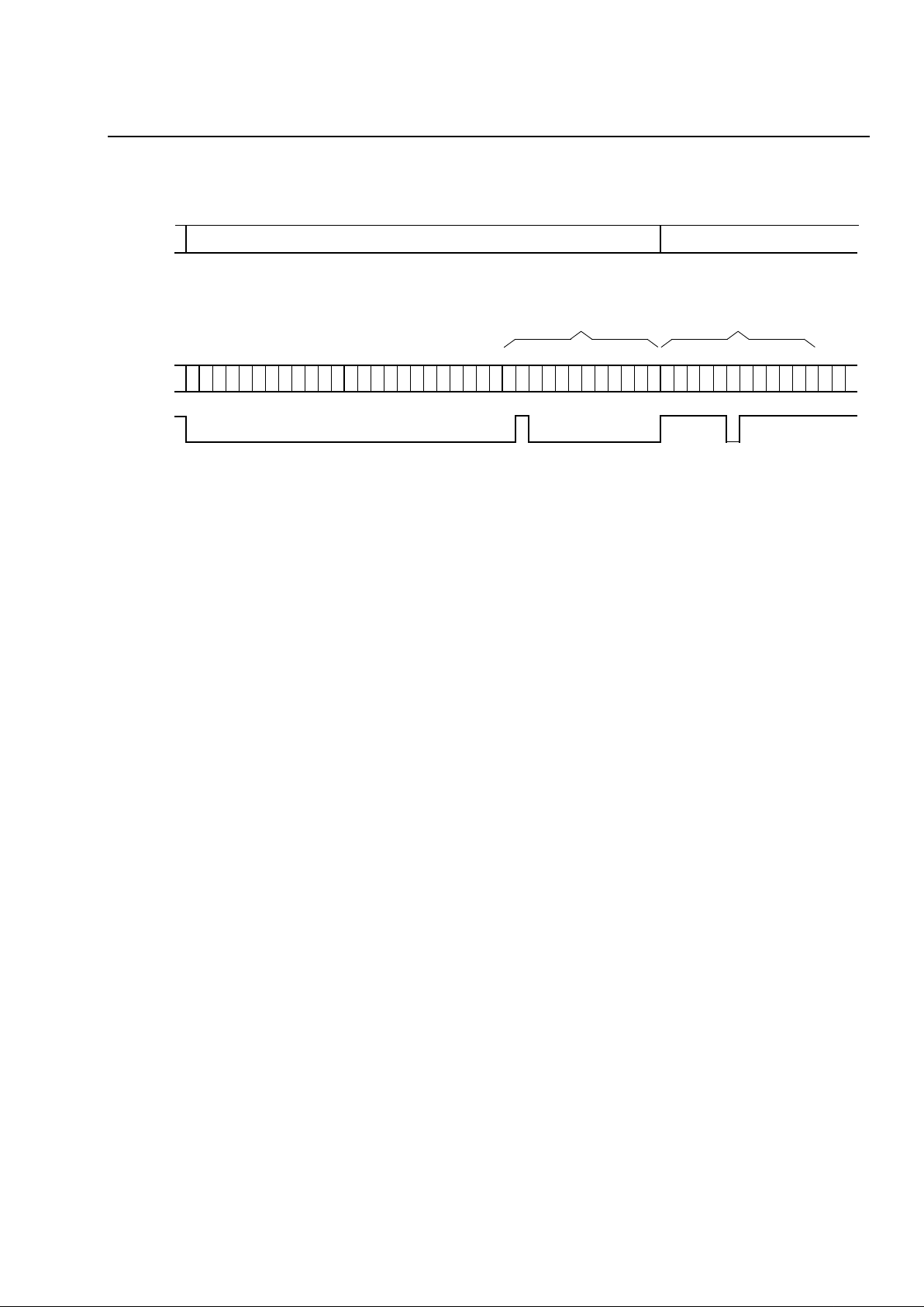
Lucent Technologies Inc. 25
Preliminary Data Sheet
ORCA
ORT4622 FPSC
March 2000 Four-Channel x 622 Mbits/s Backplane Transceiver
Lucent Technologies Inc.
Backplane Transceiver Core Detailed Description
(continued)
5-9331
Notes: SPE signal behavior shown in this figure is just for illustration purposes: SPE behavior is dependent on pointer movements and con cat-
enation.
SPE signal must be high during negative stuff opportunity byte time slots (H3) for which valid data is carried (negative stuffing).
SPE signal must be low during positive stuff opportunity byte time slots for which there is no valid data (positive stuffing).
Figure 10. SPE Stuff Bytes
STS-12 TOH ROW # 4 SPE ROW # 4
H1H1 H1H1H1 H1H1 H1 H1H1 H1 H1H2 H2H2H2 H2H2
H2H2 H2 H2H2 H2 H3H3 H3H3H3 H3H3 H3 H3H3 H3 H3
STS-12
SPE
POSITIVE STUFF
OPPORTUNITY BYTES
123456789101112
NEGATIVE STUFF
OPPORTUNITY BYTES
SPE SIGNAL SHOWS NEGATIVE STUFFING FOR 2ND STS-1,
AND POSITIVE STUFFING FOR 6TH STS-1
Powerdown Mode
Powerdown mode will be entered when the corresponding channel is disabled. Channels can be independently enabled or disabled under software control.
Parallel data bus output enable and TOH serial data
output enable signals are made available to the FPGA
logic. The HSI macrocell’s corresponding channel is
also powered down. The device will power up with all
four channels in powerdown mode.
In addition, an LVDS_EN pin has been added to control
the L VDS pins during boundary scan. During functional
operation, enabling/disabling LVDS buffers is controlled by software registers. When in boundary scan
mode, LVDS_EN controls the enabling/disabling of
LVDS buffers instead of software registers. This
LVDS_EN pin should be pulled high on the board for
functional operation, and pulled low during boundary
scan.
Redundancy and Protection Switching
The ORT4622 supports STS-12/STS-48 redundancy
by either software or hardware control for protection
switching applications. For the transmitter mode, no
additional functionality is required for redundant operation. For receiving data, STS-12 data redundancy can
be implemented within the same device, while STS-48
and above data stream requires a pair of ORT4622
devices to support redundancy.
In STS-12 mode, the channel A receive data bus port is
used for both channel A and channel B. Similarly, the
channel C receive data bus port is used for both channel C and channel D. Channel B and channel D
become the redundant channels. The channel B and
channel D receive data bus ports are unused. Soft registers provide independent control to the protection
switching MUXes for both parallel data ports and serial
TOH data ports. When direct hardware control for protection switching is needed, external protection switch
pins are available for channels A and B, and also channels C and D. The external protection switch pins only
support parallel SPE/TOH data protection switching,
but not the serial TOH data.
In STS-48 mode, two independent devices are
required to work and protect for redundancy. Parallel
and serial port output pins on the FPGA side should be
3-stated as the basis for supporting redundancy. The
existing local bus enable signals at the CIC can be
used as 3-state controls for FPGA data bus if needed,
which can be easily accessed by software control.
Users can also create their own protection switch 3state enable signals either in FPGA logic or external to
the device, depending on the specific application.

ORCA
ORT4622 FPSC
Preliminary Data Sheet
Four-Channel x 622 Mbits/s Backplane Transceiver March 2000
26 Lucent Technologies Inc.
Lucent Technologies Inc.
Memory Map
Definition of Register Types
There are six structural register elements: sreg, creg, preg, iareg, isreg, and iereg. There are no mixed registers in
the chip. This means that all bits of a particular register (particular address) are structurally the same.
Table 8
. Structural Register Elements
Registers Access and General Description
The memory map comprises three address blocks:
■
Generic register block: ID, revision, scratch pad, lock, FIFO alignment, and reset registers.
■
Device register block: control and status bits, common to the four channels.
■
Channel register blocks: each of the four channels have an address block. The four address blocks have the
exact same structure with a constant address offset between channel register blocks.
All registers are write-protected by the lock register, except for the scratch pad register. The lock register is a 16-bit
read/write register. Write access is given to registers only when the key value 0xA001 is present in the lock register.
An error flag will be set upon detecting a write access when write permission is denied. The default value is
0x0000.
After powerup reset or soft reset, unused register bits will be read as zeros. Unused address locations are also
read as zeros. Write only register bits will be read as zeros. The detailed information on register access and function are described on the tables, memory map, and memory map bit description.
Element Register Description
sreg Status Register A status register is read only, and, as the name implies, is used to convey the status
information of a particular element or function of the ORT4622 core. The reset value
of an sreg is really the reset value of the particular element or function that is being
read. In some cases, an sreg is really a fixed value. An example of which is the fixed
ID and revision registers.
creg Control Register A control register is read and writable memory element inside core control. The
value of a creg will always be the value written to it. Events inside the ORT4622 core
cannot effect creg value. The only exception is a soft reset, in which case the creg
will return to its default value. The control register have default values as defined in
the default value column of Table 9.
preg Pulse Register Each element, or bit, of a pulse register is a control or event signal that is asserted
and then deasserted when a value of one is written to it. This means that each bit is
always of value 0 until it is written to, upon which it is pulsed to the value of one and
then returned to a value of 0. A pulse register will always have a read value of 0.
iareg Interrupt Alarm
Register
Each bit of an interrupt alarm register is an event latch. When a particular event is
produced in the ORT4622 core, its occurrence is latched by its associated iareg bit.
To clear a particular iareg bit, a value of one must be written to it. In the ORT4622
core, all isreg reset values are 0.
isreg Interrupt Status
Register
Each bit of an interrupt status register is physically the logical-OR function. It is a
consolidation of lower level interrupt alarms and/or isreg bits from other registers. A
direct result of the fact that each bit of the isreg is a logical-OR function means that it
will have a read value of one if any of the consolidation signals are of value one, and
will be of value 0 if and only if all consolidation signals are of value 0. In the
ORT4622 core, all isreg default values are 0.
ereg Interrupt Enable
Register
Each bit of a status register or alarm regis ter has an associated enable bit. If this bit
is set to value one, then the event is allowed to propagate to the next higher level of
consolidation. If this bit is set to zero, then the associated iareg or isreg bit can still
be asserted but an alarm will not propagate to the next higher level. An interrupt
enable bit is an interrupt mask bit when it is set to value 0.

Lucent Technologies Inc. 27
Preliminary Data Sheet
ORCA
ORT4622 FPSC
March 2000 Four-Channel x 622 Mbits/s Backplane Transceiver
Lucent Technologies Inc.
Memory Map
(continued)
Memory Map Overview
Table 9
.
Memory Map
Notes:
1.Generic register block.
2.Device register block-Rx.
3.Device register block-Tx.
ADDR
[6:0]
Reg.
Type
DB7 DB6 DB5 DB4 DB3 DB2 DB1 DB0
Default
Value
(hex)
Notes
Generic Register Block
00 sreg fixed rev [7:0] 01 1
01 sreg fixed ID LSB [7:0] 01
02 sreg fixed ID MSB [7:0] A0
03 creg scratch pad [7:0] 00
04 creg lockreg MSB [7:0] 00
05 creg lockreg LSB [7:0] 00
06preg——————FIFO align-
ment com-
mand
global
reset
command
NA
Device Register Block
08 creg — — — Rx TOH
frame
and
Rx TOH
clock
enable
control
ext prot
sw en
ext prot
sw
function
STS-48
STS-12 sel
(unused in
ORT4622)
LVDS
lpbk
control
00 2
09 creg — — — — parallel
port output MUX
select for
ch C
parallel
port out-
put MUX
select for
ch A
serial port
output
MUX
select for
ch C
serial port
output
MUX
select for
ch A
0F
0a creg — — — FIFO aligner threshold value (min) [4:0] 02
0b creg — — — FIFO aligner threshold value (max) [4:0] 15
0c creg — scrambler/
descram-
bler
control
input/
output
parallel
bus parity
control
line loop-
back
control
number of consecutive A1/A2 errors to
generate [3:0]
60 3
0d creg A1 error insert value [7:0] 00
0e creg A2 error insert value [7:0] 00
0f creg transmitter B1 error insert mask [7:0] 00
 Loading...