

AGERE ORLI10G-3BM680, ORLI10G-2BM680, ORLI10G-3BM416, ORLI10G-1BM416, ORLI10G-2BM416 Datasheet
Data Sheet
October 2001
ORCA
®
ORLI10G Quad 2.5 Gbits/s
10 Gbits/s, and 12.5 Gbits/s Line Interface FPSC
Introduction
Agere Systems Inc. has developed a new
ORCA
Series 4 based FPSC which combines a high-speed
line interface with a flexible FPGA logic core. Built on
the Series 4 reconfigurable embedded system-onchips (SoC) architecture, the ORLI10G consists of an
OIF standard (OIF 99.102.5) compliant XSBI or
OIF-SFI4-01.0 SFI-4, 10 G bits/s or 12.5 Gbits/s
transmit and 10 Gbits/s or 12.5 Gbits/s receive line
interface. Both transmit and receive interfaces consist of 16-bit LVDS data up to 850 Mbit s/s , inte grat ed
transmit and receive programmable PLLs for data
rate conversions between the line-side and systemside data rates, and a programmable logic interface
at the system end for use with SONET/SDH, Ethernet, or OTN/digital wrapper with strong FEC system
device data standards. In addition to the embedded
functionality, the device will include up to 400k of
usable FPGA gates. The line interface includes logic
to divide the data rate down to 212 MHz or less
(1/4 line rate) or 106 MHz or less (1/8 line rate) for
transfer to the FPGA logic. The ORLI10G is designed
to connect directly to Agere’s 10 Gbits/s TTRN0110G
MUX and TRCV0110G deMUX or Agere’s
12.5 Gbits/s TTRN0126 MUX and TRCV01126
deMUX on the line side, as well as other industrystandard devices. The programmable logic interface
on the system side allows for direct connection to a
10 Gbits/s Ethernet MAC, a 10 Gbits/s SONET/SDH
framer/data engine, or a 10 Gbits/s/12.5 Gbits/s digital wrapper/FEC framer/data engine.
For 10 Gbits/s Ethernet, the ORLI10G supports the
physical coding sublayer (PCS), interfaces to the
physical media attachment (PMA), and connects to
the system interface (host or switch) for the proposed
IEEE
®
802.3ae 10 Gbits/s serial LAN PHY.
The ORLI10G FPSC is a high-speed programmable
device for 10G/s data solutions. It can be used as the
interface between the line interface and the system
interface in a variety of emerging networks, including
10 Gbits/s SONET/SDH (OC-192/STM-48),
10 Gbits/s optical transport networks (OTN) using
digital wrapper and strong FEC, or 10 Gbits/s Ethernet. Other functions include use in Quad OC-48/
STM-16 SONET/SDH systems, interfaces between
Quad OC-48/STM-16 and OC-192/STM-64 components, and use as a generic data transfer mechanism
between two devices at 10 Gbits/s rates. Data is
received at the line interface and then sent to either a
4-bit or 8-bit serial-to-parallel converter. On the transmit interface, either a 4-bit or 8-bit parallel-to-serial
converter is used. Thus, the data rate at the internal
FPGA interface is either 1/4 or 1/8 the line rate.
The programmable PLLs on the ORLI10G provide for
great flexibility in handling clock rate conversion due
to differing amounts of overhead bits in various system data standards. For example, the ORLI10G can
divide down the STS-192/STM-64 SONET/SDH data
line rate of 622 MHz by 4 to synchronize with a
155 MHz system clock, or the 12.5 Gbits/s SuperFEC data line rate of 781 MHz can be divided by 8 to
98 MHz system clock or by 8 x 4/5 to provide a
78 MHz system data rate.
Table 1.
ORCA
ORLI10G—Available FPGA Logic
* 192 user I/Os for the 416 PBGAM package and 316 user I/Os for the 680 PBGAM package are available out of the 432 possible user
I/Os.
Note: The embedded core and interface are not included in the above gate counts. The usable gate counts range from a logic-only gate
count to a gate count assuming 20% of the PFUs/SLICs being used as RAMs. The logic-only gate count includes each PFU/SLIC
(counted as 108 gates/PFU), including 12 gates per LUT/FF pair (eight per PFU), and 12 gates per SLIC/FF pair (one per PFU).
Each of the four PIO groups are counted as 16 gates (three FFs, fast-capture latch, output logic, CLK, and I/O buffers). PFUs used
as RAM are counted at four gates per bit, with each PFU capable of implementing a 32 x 4 RAM (or 512 gates) per PFU. Embedded
block RAM (EBR) is counted as four gates per bit, plus each block has an additional 25k gates. 7k gates are used for each PLL and
50k gates for the embedded system bus and microprocessor interface logic. Both the EBR and PLLs are conservatively utilized in
the gate count calculations.
Device PFU
Rows
PFU
Columns
Total
PFUs
User I/Os
*
LUTs EBR
Blocks
EBR Bits
(k)
Usable
Gates (k)
ORLI10G 36 36 1296 432 10,368 12 111 380—800

Table of Contents
Contents Page Contents Page
2 Agere Systems Inc.
Data Sheet
October 2001
10 Gbits/s, a nd 12.5 Gbits/s Line Interface FPSC
ORCA
ORLI10G Quad 2.5 Gbits/s
Introduction..................................................................1
Embedded Function Features .....................................4
Intellectual Property Features......................................4
Programmable Features..............................................4
Programmable Logic System Features .......................6
Description...................................................................7
FPSC Definition ........................................................7
FPSC Overview ........................................................7
FPSC Gate Counting ................................................7
FPGA/Embedded Core Interface..............................7
ORCA Foundry Development System ......................7
FPSC Design Kit.......................................................8
FPGA Logic Overview...............................................8
PLC Logic .................................................................8
Programmable I/O.....................................................9
Routing......................................................................9
System-Level Features..............................................10
Microprocessor Interface ........................................10
System Bus.............................................................10
Phase-Locked Loops .................... ...... ....... .............10
Embedded Block RAM............................................10
Configuration...........................................................11
Additional Information .............................................11
ORLI10G Overview ...................................................11
Device Layout .........................................................11
10G Mode ...............................................................11
2.5G Mode ..............................................................12
Receive Path Details .................................................15
Line Interface ..........................................................15
DeMUX ...................................................................15
Onboard Receive PLLs...........................................15
Transmit Path Details ................................................17
MUX........................................................................17
Onboard Transmit PLLs..........................................17
Line Interface ..........................................................17
ORLI10G Demultiplexer (Rx) Detail ..........................19
ORLI10G Multiplexer (Tx) Detail ...............................25
ORLI10G Embedded PLLs........................................31
ORLI10G Embedded Programmable PLLs
Specifications ........................................................... 32
ORLI10G Reset Requirements................................. 32
Line Interface Circuit Specifications ......................... 33
Power Supply Decoupling LC Circuit..................... 33
XGMII ORCA 4E Receive Analysis .......................... 34
XGMII Considerations............................................ 34
Absolute Maximum Ratings...................................... 35
Recommended Operating Conditions ...................... 35
Embedded Core LVDS I/O ....................................... 36
LVDS Receiver Buffer Requirements..................... 37
Timing Characteristics.............................................. 38
Receive Input Data Interface............ ...... ....... ...... ... 38
Transmit STS-48/STS-192 (2.5G/10G) Data
Outputs..................................................................... 39
Input/Output Buffer Measurement Conditions
(Non-LVDS Buffer) ................................................... 40
LVDS Buffer Characteristics.................................. ... 41
Termination Resistor.............................................. 41
LVDS Driver Buffer Capabilities............................. 41
Pin Information ......................................................... 42
Package Pinouts .................................................... 47
Package Thermal Characteristics Summary ............ 65
Θ
JA........................................................................ 65
ψ
JC ........................................................................ 65
Θ
JC........................................................................ 65
Θ
JB........................................................................ 65
FPSC Maximum Junction Temperature................. 65
Package Thermal Characteristics............................. 66
Heat Sink Vendors for BGA Packages..................... 66
Package Coplanarity ................................................ 66
Package Parasitics................................................... 67
Package Outline Diagrams....................................... 68
Terms and Definitions ............................................ 68
416-Pin PBGAM..................................................... 69
680-Pin PBGAM..................................................... 70
Hardware Ordering Information................................ 71
Software Ordering Information ................................. 71

Agere Systems Inc. 3
Data Sheet
October 2001
Table of Contents
(continued)
List of Figures Page List of Tables Page
10 Gbits/s, and 12.5 Gbits/s Line Interface FPSC
ORCA ORLI10G Quad 2.5 Gbits/s
Figure 1. ORCA ORLI10G Block Diagram ...............13
Figure 2. 10G (Single-Channel) and 2.5G
(Quad-Channel) Modes .........................................14
Figure 3. ORLI10G Embedded Core Rece ive
Path Diagram .........................................................16
Figure 4. ORLI10G Embedded Core Transmit Path
Diagram .................................................................18
Figure 5. Demultiplexer Output Data Structure ........20
Figure 6. Demultiplexer Serial-to-Parallel
Conversion—Divide by 8, 10G Mode .....................21
Figure 7. Demultiplexer Serial-to-Parallel
Conversion—Divide by 4, 10G Mode .....................22
Figure 8. Demultiplexer Serial-to-Parallel
Conversion—Divide by 8, 2.5G Mode ....................23
Figure 9. Demultiplexer Serial-to-Parallel
Conversion—Divide by 4, 2.5G Mode ....................24
Figure 10. Multiplexer Input Data Structure ..............26
Figure 11. Multiplexer Parallel-to-Serial
Conversion—Divide by 8, 10G Mode .....................27
Figure 12. Multiplexer Parallel-to-Serial
Conversion—Divide by 4, 10G Mode .....................28
Figure 13. Multiplexer Parallel-to-Serial
Conversion—Divide by 8, 2.5G Mode ....................29
Figure 14. Multiplexer Parallel-to-Serial
Conversion—Divide by 4, 2.5G Mode ....................30
Figure 15. ORLI10G Programmable PLL Block
Diagram .................................................................31
Figure 16. Sample Power Supply Filter Network for
Analog LI Power Supply Pins .................................33
Figure 17. Simplified XGMII Block Diagram .............34
Figure 18. Receive Input Data Timing ......................38
Figure 19. Transmit Output Data Timing ..................39
Figure 20. ac Test Loads ..........................................40
Figure 21. Output Buffer Delays ...............................40
Figure 22. Input Buffer Delays ..................................40
Figure 23. LVDS Driver and Receiver and Associated
Internal Components ..............................................41
Figure 24. LVDS Driver and Receiver ......................41
Figure 25. LVDS Driver ............................................41
Figure 26. Package Parasitics ..................................67
Table 1. ORCA ORLI10G—Available FPGA Logic ... 1
Table 2. Programmable PLL Specifications ............ 32
Table 3. ORLI10G Reset Requirements .................. 32
Table 4. HSTL Input Requirements to FPGA .......... 35
Table 5. Absolute Maximum Ratings ....................... 35
Table 6. Recommended Operating Conditions ....... 35
Table 7. Driver dc Data ............................................ 36
Table 8. Driver ac Data ............................................ 36
Table 9. Driver Power Consumption ........................ 36
Table 10. Receiver ac Data ..................................... 37
Table 11. Receiver Power Consumption ................. 37
Table 12. Receiver dc Data ..................................... 37
Table 13. LVDS Operating Parameters ................... 37
Table 14. Receive Data Input Timing ...................... 38
Table 15. Transmit Data Output Timing .................. 39
Table 16. FPGA Common-Function Pin
Description ............................................................ 42
Table 17. FPSC Function Pin Description ............... 45
Table 18. Embedded Core/FPGA Interface Signal
Description ............................................................ 46
Table 19. ORCA Programmable I/Os Summary ...... 47
Table 20. PBGA Pinout Table ................................. 48
Table 21. ORCA ORLI10G Plastic Package
Thermal Guidelines ............................................... 66
Table 22. Heat Sink Vendors ................................... 66
Table 23. . ORCA ORLI10G Package Parasitics .... 67
Table 24. Device Type Options ............................... 71
Table 25. Temperature Options ............................... 71
Table 26. Package Options ..................................... 71
Table 27. Package Matrix (Speed Grade) ............... 71

44 Agere Systems Inc.
Data Sheet
October 2001
10 Gbits/s, a nd 12.5 Gbits/s Line Interface FPSC
ORCA ORLI10G Quad 2.5 Gbits/s
Embedded Function Features
■
Provides a line interface-to-interface with various
system standards such as OC-192/STM-64 SONET/
SDH, Quad OC-48/STM-16 10 Gbits/s Ethernet, and
10 Gbits/s OTN (digital wrapper/strong FEC) or
12.5 Gbits/s SuperFEC.
■
Embedded PLLs with programma ble M/N
multiplication/division values provide for flexible data
rate conversion between line side and system side.
■
Line side provides for 16-bit LVDS data with multiple
line frequencies supported up to 850 MHz,
depending on system standard.
■
Line side interface, including timing and jitter
specifications, compliant to OIF 99.102.5 standard.
■
Receive side interface can be split into four separate
asynchronous 2.5 Gbits/s interfaces (4-bit LVDS data
interface for each) with a separate clock for each for
transfer to the FPGA logic.
■
Data and clock rates divided by 4 or 8 for use in
FPGA logic.
■
Direct interface to Agere’s 10 Gbits/s MUX
(TTRN0110G) and deMUX (TRCV0110G) or
12.5 Gbits/s MUX (TTRN01126) and deMUX
(TRCV01126) for XSBI, SFI-4, or SuperFEC
applications.
■
LVDS I/Os compliant with EIA®-644 support hot
insertion. All embedded LVDS I/Os include both input
and output on-board termination to allow high-speed
operation.
■
Low-power LVDS buffers.
Intellectual Property Features
Programmable logic provides a variety of yet-to-be
standardized interface functions, including the
following IP core functions:
■
10 Gbits/s Ethernet as defined by IEEE 802.3ae:
— XGMII for interfacing to 10 Gbits/s Ethernet
MACs. XGMII is a 156 MHz double data rate
parallel short-reach (typically less than 2 in.)
interconnect interfac e.
— Elastic store buffers for clock domain transfer to/
from the XGMII interface.
— X
59
+ X39 + X1 scrambler/descrambler for
10 Gbits/s Ethernet.
— 64b/66b encoders/decoders for 10 Gbits/s
Ethernet.
■
POS-PHY4 interface for 10 Gbits/s SONET/SDH and
OTN systems and some 10 Gbits/s Ethernet
systems.
■
Quad 2.5 Gbits/s SONET/SDH to 10 Gbits/s SONET/
SDH MUX/deMUX functions.
■
66-bit word aligner and 64b/66b receive path
decoder, 64b/66b transmit path encoder, and
66b/64b transmit path conversion for Ethernet
overhead bits.
Programmable Features
■
High-performance programmable logic:
— 0.16 µm 7-level metal technology.
— Internal performance of >250 MHz.
— 400k usable system gates.
— Meets multiple I/O interface standards.
— 1.5 V operation (30% less power than 1.8 V
operation) translates to greater performance.
■
Traditional I/O selections:
— LVTTL and LVCMOS (3.3 V, 2.5 V, and 1.8 V)
I/Os.
— Per pin-selectable I/O clamping diodes provide
3.3 V PCI compliance.
— Individually programmable drive capability:
24 mA sink/12 mA source, 12 mA sink/6 mA
source, or 6 mA sink/3 mA source.
— Two slew rates supported (fast and slew limited).
— Fast-capture input latch and input flip-flop (FF)
latch for reduced input setup time and zero hold
time.
— Fast open-drain drive capability.
— Capability to register 3-state enable signal.
— Off-chip clock drive capability.
— Two input function generator in output path.
■
New programmable high-speed I /O:
— Single-ended: GTL, GTL+, PECL, SSTL3/2
(class I & II), HSTL (Class I, III, IV), ZBT, and
DDR.
— Double-ended: LVDS, bused-LVDS, LVPECL.
Programmable parallel termination (100 Ω) also
supported for these I/Os.
— Customer-defined: ability to substitute arbitrary
standard cell I/O to meet fast-moving standards.
■
New capability to (de)multiplex I/O signals:
— New DDR on both input and output at rates up to
311 MHz (622 MHz effective rate).
— New 2x and 4x downlink and uplink capability per
I/O (i.e., 50 MHz internal to 200 MHz I/O).

Agere Systems Inc. 5
Data Sheet
October 2001
10 Gbits/s, and 12.5 Gbits/s Line Interface FPSC
ORCA ORLI10G Quad 2.5 Gbits/s
Programmable Features
(continued)
■
Enhanced twin-quad programmable function unit
(PFU):
— Eight 16-bit look-up tables (LUTs) per PF U.
— Nine user registers per PFU, one following each
LUT, and organized to allow two nibbles to act
independently, plus one extra for arithmetic operations.
— New register control in each PFU has two inde-
pendent programmable clocks, clock enables,
local set/reset, and data selects.
— New LUT structure allows flexible combinations of
LUT4, LUT5, new LUT6, 4
→
1 MUX, new
8 → 1 MUX, and ripple mode arithmetic functions
in the same PFU.
— 32 x 4 RAM per PFU, configurable as single- or
dual-port. Create large, fast RAM/ROM blocks
(128 x 8 in only eight PFUs) using the SLIC
decoders as bank drivers.
— Soft-wired LUT s (SWL) allow fast cascading of up
to three levels of LUT logic in a single PFU
through fast internal routing which reduces routing
congestion and improves speed.
— Flexible fast access to PFU inputs from routing.
— Fast-carry logic and routing to all four adjacent
PFUs for nibble-wide, byte-wide, or longer arithmetic functions, with the option to register the PFU
carry-out.
■
Abundant high-speed buffered and nonbuffered
routing resources provide 2x average speed
improvements over previous architectures.
■
Hierarchical routing optimized for both local and
global routing with dedicated routing resources. This
results in faster routing times with predictable and
efficient performance.
■
SLIC provides eight 3-stable buffers, up to a 10-bit
decoder, and PAL™-like and-or-invert (AOI) in each
programmable logic cell.
■
New 200 MHz embedded quad-port RAM blocks,
two read ports, two write ports, and two sets of byte
lane enables. Each embedded RAM block can be
configured as:
— 1—512 x 18 (quad-port, two read/two write) with
optional built-in arbitrati on.
— 1—256 x 36 (dual-port, one read/one write).
— 1—1k x 9 (dual-port, one read/one write).
— 2—512 x 9 (dual-port, one read/one write for
each).
— 2 RAMs with arbitrary number of words whose
sum is 512 or less by 18 (dual-port, one read/one
write).
— Supports joining of RAM blocks.
— Two 16 x 8-bit content addressable memory
(CAM) support.
— FIFO 512 x 18, 256 x 36, 1k x 9, or dual 512 x 9.
— Constant multiply (8 x 16 or 16 x 8).
— Dual variable multiply (8 x 8).
■
Embedded 32-bit internal system bus plus 4-bit
parity interconnects FPGA logic, microprocessor
interface (MPI), embedded RAM blocks, and
embedded standard cell blocks with 100 MHz bus
performance. Included are built-in system registers
that act as the control and status center for the
device.
■
Built-in testability:
— Full boundary scan (IEEE 1149.1 and draft 1 149.2
JTAG) for the programmable I/Os only.
— Programming and readback through boundary-
scan port compliant to IEEE Draft 1532:D1.7.
— TS_ALL testability function to 3-state all I/O pins.
— New temperature-sensing diode.
■
Improved built-in clock management with
programmable phase-locked loops (PPLLs) provides
optimum clock modification and conditioning for
phase, frequency, and duty cycle from 20 MHz up to
420 MHz. Multiplication of input frequency up to 64x
and division of input frequency down to 1/64x
possible.
■
New cycle stealing capability allows a typical 15% to
40% internal speed improvement after final place
and route. This feature also enables compliance with
many setup/hold and clock to out I/O specifications
and may provide reduced ground bounce for output
buses by allowing flexible delays of switching output
buffers.

66 Agere Systems Inc.
Data Sheet
October 2001
10 Gbits/s, a nd 12.5 Gbits/s Line Interface FPSC
ORCA ORLI10G Quad 2.5 Gbits/s
Programmable Logic System Features
■
PCI local bus compliant for FPGA I/Os.
■
Improved PowerPC®/PowerQUICC 860 and
PowerPC/PowerQUICC II MPC8260 high-s pee d
synchronous microprocessor interface can be used
for configuration, readback, device control, and
device status, as well as for a general-purpose
interface to the FPGA logic, RAMs, and embedded
standard-cell blocks. Glueless interface to
synchronous PowerPC processors with userconfigurable address space provided.
■
New embedded AMBA™ specification 2.0 AHB
system bus (ARM
®
processor) facilitates
communication among the microprocessor interface,
configuration logic, embedded block RAM, FPGA
logic, and embedded standard cell blocks.
■
Variable-size bused readback of configuration data
capability with the built-in microprocessor interface
and system bus.
■
Internal, 3-state, and bidirectional buses with simple
control provided by the SLIC.
■
New clock routing structures for global and local
clocking significantly increases speed and reduces
skew (<200 ps for OR4E4).
■
New local clock routing structures allow creation of
localized clock trees.
■
Two new edge clock structures allow up to six highspeed clocks on each edge of the device for
improved setup/hold and clock to out performance.
■
New double-data rate (DDR) and zero-bus turnaround (ZBT) memory interfaces support the latest
high-speed memory interfaces.
■
New 2x/4x uplink and downlink I/O capabilities
interface high-speed external I/Os to reduced-speed
internal logic.
■
ORCA Foundry development system software.
Supported by industry-standard CAE tools for design
entry, synthesis, simulation, and timing analysis.
■
Meets universal test and opera tion s PHY interfac e
for ATM (UTOPIA) Levels 1, 2, and 3 as well as
POS-PHY3. Also meets proposed specifications for
UTOPIA Level 4 and POS-PHY4 for 10 Gbits/s
interfaces.
■
Meets POS-PHY3 (2.5 Gbits/s) and POS-PHY4
(10 Gbits/s) interface standards for packet-overSONET as defined by the Saturn Group.

Agere Systems Inc. 7
Data Sheet
October 2001
10 Gbits/s, and 12.5 Gbits/s Line Interface FPSC
ORCA ORLI10G Quad 2.5 Gbits/s
Description
FPSC Definition
FPSCs, or field-programmable system chips, are
devices that combine field-programmable logic with
ASIC or mask-programmed logic on a single device.
FPSCs provide the time to market and the flexibility of
FPGAs, the design effort savings of using soft intellectual property (IP) cores, and the speed, design density,
and economy of ASICs.
FPSC Overview
Agere’s Series 4 FPSCs are created from Series 4
ORCA FPGAs. T o create a Series 4 FPSC, several columns of programmable logic cells (see FPGA Logic
Overview section for FPGA logic details) are added to
an embedded logic core. Other than replacing some
FPGA gates with ASIC gates, at greater than 10:1 efficiency, none of the FPGA functionality is changed—all
of the Series 4 FPGA capability is retained: embedded
block RAMs, MPI, PCMs, boundary scan, etc. The columns of programmable logic are replaced at the right
of the device, allowing pins from the replaced columns
to be used as I/O pins for the embedded core. The
remainder of the device pins retain their FPGA functionality.
The embedded cores can take many forms and generally come from Agere’s ASIC libraries. Other offerings
allow customers to supply their own core functions for
the creation of custom FPSCs.
FPSC Gate Counting
The total gate count for an FPSC is the sum of its
embedded core (standard-cell/ASIC gates) and its
FPGA gates. Because FPGA gates are generally
expressed as a usable range with a nominal value, the
total FPSC gate count is sometimes expressed in the
same manner. Standard-cell ASIC gates are, however,
10 to 25 times more silicon-area efficient than FPGA
gates. Therefore, an FPSC with an embedded function
is gate equivalent to an FPGA with a much larger gate
count.
FPGA/Embedded Core Interface
The interface between the FPGA logic and the embedded core has been enhanced to allow for a greater
number of interface signals than on previous FPSC
architectures. Compared to bringing embedded core
signals off-chip, this on-chip interface is much faster
and requires less power. All of the delays for the interface are precharacterized and accounted for in the
ORCA Foundry Development System.
Series 4 based FPSCs expand this int er face by pro viding a link between the embedded block and the multimaster 32-bit system bus in the FPGA logic. This system bus allows the core easy access to many of the
FPGA logic functions, including the embedded block
RAMs and the microprocessor interface.
Clock spines also can pass across the FPGA/embedded core boundary. This allows for fast, low-skew
clocking between the FPGA and the embedded core.
Many of the special signals from the FPGA, such as
DONE and global set/reset, are also available to the
embedded core, making it possible to fully integrate the
embedded core with the FPGA as a system.
For even greater system flexibility, FPGA configuration
RAMs are available for use by the embedded core.
This allows for user-p rogrammable options in the
embedded core, in turn allowing for greater flexibility.
Multiple embedded core configurations may be
designed into a single device with user-programmable
control over which configurations are implemented, as
well as the capability to change core functionality simply by reconfiguring the device.
ORCA
Foundry Development System
The ORCA Foundry development system is used to
process a design from a netlist to a configur ed FPG A.
This system is used to map a design onto the ORCA
architecture and then place and route it using ORCA
Foundry’s timing-driven tools. The development system also includes interfaces to, and libraries for, other
popular CAE tools for design entry, synthesis, simulation, and timing analysis.
The ORCA Foundry development system interfaces to
front-end design entry tools and provides the tools to
produce a configured FPGA. In the design flow, the
user defines the functionality of the FPGA at two points
in the design flow: design entry and the bit stream generation stage. Recent improvements in ORCA Foundry
allow the user to provide timing requirement information through logical preferences only; thus, the
designer is not required to have physical knowledge of
the implementation.

88 Agere Systems Inc.
Data Sheet
October 2001
10 Gbits/s, a nd 12.5 Gbits/s Line Interface FPSC
ORCA ORLI10G Quad 2.5 Gbits/s
Description
(continued)
Following design entry, the development system’s map,
place, and route tools translate the netlist into a routed
FPGA. A floor planner is available for layout feedback
and control. A static timing analysis tool is provided to
determine design speed, and a back-annotated netlist
can be created to allow simulation and timing.
Timing and simulation output files from ORCA Foundry
are also compatible with many third-party analysis
tools. A bit stream generator is then used to generate
the configuration data which is loaded into the FPGAs
internal configuration RAM, embedded block RAM,
and/or FPSC memory.
When using the bit stream generator, the user selects
options that affect the functionality of the FPGA. Combined with the front-end tools, ORCA Foundry produces configuration data that implements the various
logic and routing options discussed in this data sheet.
FPSC Design Kit
Development is facilitated by an FPSC design kit
which, together with ORCA Foundry and third-party
synthesis and simulation engines, provides all software
and documentation required to design and verify an
FPSC implementation. Included in the kit are the FPSC
configuration manager, Synopsys Smart Model
®
, and
complete online documentation. The kit's software couples with ORCA Foundry, providing a seamless FPSC
design environment. More information can be obtained
by visiting the ORCA website or contacting a local
sales office, both listed on the last page of this document.
FPGA Logic Overview
The ORCA Series 4 architecture is a new generation of
SRAM-based programmable devices fr om Agere. It
includes enhancements and innovations geared
toward today’s high-speed systems on a single chip.
Designed with networking applications in mind, the
Series 4 family incorporates system-level features that
can further reduce logic requirements and increase
system speed. ORCA Series 4 devices contain many
new patented enhancements and are offered in a variety of packages and speed grades.
The hierarchical architecture of the logic, clocks, routing, RAM, and system-level blocks create a seamless
merge of FPGA and ASIC designs. Modula r hardwa re
and software technologies enable system-on-chip integration with true plug-and-play design implementation.
The architecture consists of four basic elements: programmable logic cells (PLCs), programmable I/O cells
(PIOs), embedded block RAMs (EBRs), and systemlevel features. These elements are interconnected with
a rich routing fabric of both global and local wires. An
array of PLCs are surrounded by common interface
blocks which provide an abundant interface to the adjacent PLCs or system blocks. Routing congestion
around these critical blocks is eliminated by the use of
the same routing fabric implemented within the programmable logic core. Each PLC contains a PFU,
SLIC, local routing resources, and configuration RAM.
Most of the FPGA logic is performed in the PFU, but
decoders, PAL-like functions, and 3-state buffering can
be performed in the SLIC. The PIOs provide device
inputs and outputs and can be used to register signals
and to perform input demultiplexing, output multiplexing, uplink and downlink functions, and other functions
on two output signals. Large blocks of 512 x 18 quadport RAM complement the existing distributed PFU
memory. The RAM blocks can be used to implement
RAM, ROM, FIFO, multiplier, and CAM. Some of the
other system-level functions include the MPI, PLLs,
and the embedded system bus (ESB).
PLC Logic
Each PFU within a PLC contains eight 4-input (16-bit)
LUTs, eight latches/FFs, and one additional flip-flop
that may be used independently or with arithmetic functions.
The PFU is organized in a twin-quad fashion; two sets
of four LUTs and FFs that can be controlled independently. Each PFU has two independent programmable
clocks, clock en able s, loca l set/ rese t, an d dat a sele cts.
LUTs may also be combined for use in arithmetic functions using fast-carry chain logic in either 4-bit or 8-bit
modes. The carry-out of either mode may be registered
in the ninth FF for pipelining. Each PFU may also be
configured as a synchronous 32 x 4 single- or dual-port
RAM or ROM. The FFs (or latches) may obtain input
from LUT out puts or dire ctly f rom in verti ble PFU i nputs,
or they can be tied high or tied low. The FFs also have
programmable clock polarity, clock enables, and local
set/reset.

Agere Systems Inc. 9
Data Sheet
October 2001
10 Gbits/s, and 12.5 Gbits/s Line Interface FPSC
ORCA ORLI10G Quad 2.5 Gbits/s
Description
(continued)
The SLIC is connected from PLC routing resources
and from the outputs of the PFU. It contains eight
3-state, bidirectional buffers, and logic to perform up to
a 10-bit AND function for decoding, or an AND-OR with
optional INVERT to perform PAL-like functions. The
3-state drivers in the SLIC and their direct connections
from the PFU outputs make fast, true, 3-state buses
possible within the FPGA, reducing required routing
and allowing for real-world system performance.
Programmable I/O
The Series 4 PIO addresses the demand for the flexibility to select I/Os that meet system interface requirements. I/Os can be programmed in the same manner
as in previous ORCA devices, with the additional new
features that allow the user the flexibility to select new
I/O types that support high-speed interfaces.
Each PIO contains four programmable I/O pads and is
interfaced through a common interface block to the
FPGA array. The PIO is split into two pairs of I/O pads
with each pair having independent clock enables, local
set/reset, and global set/reset. On the input side, each
PIO contains a programmable latch/flip-flop which
enables very fast latching of data from any pad. The
combination provides for very low setup requirements
and zero hold times for signals coming on-chip. It may
also be used to demultiplex an input signal, such as a
multiplexed address/data signal, and register the signals without explicitly building a demultiplexer with a
PFU.
On the output side of each PIO, an output from the
PLC array can be routed to each output flip-flop, and
logic can be associated with each I/O pad. The output
logic associated with each pad allows for multiplexing
of output signals and other functions of two output signals.
The output FF, in combination with output signal multiplexing, is particularly useful for registering address
signals to be multiplexed with data, allowing a full clock
cycle for the data to propagate to the output. The output buffer signal can be inverted, and the 3-state control can be made active-high, active-low, or always
enabled. In addition, this 3-state signal can be registered or nonregistered.
The Series 4 I/O logic has been enhanced to include
modes for speed uplink and downlink capabilities.
These modes are supported through shift register
logic, which divides down incoming data rates or multiplies up outgoing data rates. This new logic block also
supports high-speed DDR mode requirements where
data is clocked into and out of the I/O buffers on both
edges of the clock.
The new programmable I/O cell allows designers to
select I/Os which meet many new communication standards, permitting the device to hook up directly without
any external interface translation. They support traditional FPGA standards as well as high-speed, singleended, and differential-pair signaling (as shown in
Table 1). Based on a programmable, bank-oriented I/O
ring architecture, designs can be implemented using
3.3 V, 2.5 V, 1.8 V, and 1.5 V referenced output levels.
Routing
The abundant routing resources of the Series 4 architecture are organized to route signals individually or as
buses with related control signals. Both local and global signals utilize high-speed buffered and nonbuffered
routes. One PLC segmented (x1), six PLC segmented
(x6), and bused half-chip (xHL) routes are patterned
together to provide high connectivity with fast software
routing times and high-speed system performance.
Eight fully distributed primary clocks are routed on a
low-skew, high-speed distribution network and may be
sourced from dedicated I/O pads, PLLs, or the PLC
logic. Secondary and edge-clock routing are available
for fast regional clock or control signal routing for both
internal regions and on device edges. Secondary clock
routing can be sourced from any I/O pin, PLLs, or the
PLC logic.
The improved routing resources offer great flexibility in
moving signals to and from the logic core. This flexibility translates into an improved capability to route
designs at the required speeds when the I/O signals
have been locked to specific pins.

1010 Agere Systems Inc.
Data Sheet
October 2001
10 Gbits/s, a nd 12.5 Gbits/s Line Interface FPSC
ORCA ORLI10G Quad 2.5 Gbits/s
System-Level Features
The Series 4 also provides system-level functionality
by means of its microprocessor interface, embedded
system bus, quad-port embedded block RAMs,
universal programmable phase-locked loops, and the
addition of highly tuned networking specific phaselocked loops. These functional blocks allow for easy
glueless system interfacing and the capability to adjust
to varying conditions in today’s high-speed networking
systems.
Microprocessor Interface
The MPI provides a glueless interface between the
FPGA and PowerPC microprocessors. Programmable
in 8-, 16-, and 32-bit interfaces with optional parity to
the Motorola
®
PowerPC 860 bus, it can be used for
configuration and readback, as well as for FPGA control and monitoring of FPGA status. All MPI transactions utilize the Series 4 embedded system bus at
66 MHz performance.
A system-level microprocessor interface to the FPGA
user-defined logic following configuration, through the
system bus, including access to the embedded block
RAM and general user-logic, is provided by the MPI.
The MPI supports burst data read and write transfers,
allowing short, uneven transmission of data through
the interface by including data FIFOs. Transfer
accesses can be single beat (1 x 4 bytes or less),
4-beat (4 x 4 bytes), 8-beat (8 x 2 bytes), or 16-beat
(16 x 1 bytes).
System Bus
An on-chip, multimaster, 8-bit system bus with 1-bit
parity facilitates communication among the MPI, configuration logic, FPGA control, and status registers,
embedded block RAMs, as well as user logic. Utilizing
the AMBA specification Rev 2.0 AHB protocol, the
embedded system bus offers arbiter, decoder, master,
and slave elements.
The system bus control registers can provide control to
the FPGA such as signaling for reprogramming, reset
functions, and PLL programming. Status registers
monitor INIT, DONE, and system bus errors. An
interrupt controller is integrated to provide up to eight
possible interrupt resources. Bus clock generation can
be sourced from the microprocessor interface clock,
configuration clock (for slave configuration modes),
internal oscillator, user clock from routing, or port clock
(for JTAG configuration modes).
Phase-Locked Loops
Up to eight PLLs are provided on each Series 4 device,
with four PLLs generally provided for FPSCs. Programmable PLLs can be used to manipulate the frequency,
phase, and duty cycle of a clock signal. Each PPLL is
capable of manipulating and conditioning clocks from
20 MHz to 420 MHz. Frequencies can be adjusted from
1/8x to 8x, the input clock frequency. Each programmable PLL provides two outputs that have different multiplication factors but can have the same phas e
relationships. Duty cycles and phase delays can be
adjusted in 12.5% of the clock period increments. An
automatic input buffer delay compensation mode is
available for phase delay . Each PPLL provides two outputs that can have programmable (12.5% steps) phase
differences.
Additional highly tuned and characterized, dedicated
phase-locked loops (DPLLs) are included to ease system designs. These DPLLs meet ITU-T G.811 primaryclocking specifications and enable system designers to
very tightly target specified clock conditioning not traditionally available in the universal PPLLs. Initial DPLLs
are targeted to low-speed networking DS1 and E1, and
also high-speed SONET/SDH networking STS-3 and
STM-1 systems.
Embedded Block RAM
New 512 x 18 quad-port RAM blocks are embedded in
the FPGA core to significantly increase the amount of
memory and complement the distributed PFU memories. The EBRs include two write ports, two read ports,
and two byte lane enables which provide four-port
operation. Optional arbitration between the two write
ports is available, as well as direct connection to the
high-speed system bus.
Additional logic has been incorporated to allow
significant flexibil ity for FIFO, co nstant multiply, and
two-variable multiply functions. The user can configure
FIFO blocks with flexible depths of 512k, 256k, and 1k,
including asynchronous and synchronous modes and
programmable status and error flags. Multiplier
capabilities allow a multiple of an 8-bit number with a
16-bit fixed coefficient or vice versa (24-bit output), or a
multiply of two 8-bit numbers (16-bit output). On-the-fly
coefficient modifications are available through the
second read/write port. Two 16 x 8-bit CAMs per
embedded block can be implemented in single match,
multiple mat ch, and clear modes. The EBRs can also
be preloaded at device configuration time.

Agere Systems Inc. 11
Data Sheet
October 2001
10 Gbits/s, and 12.5 Gbits/s Line Interface FPSC
ORCA ORLI10G Quad 2.5 Gbits/s
System-Level Features
(continued)
Configuration
The FPGAs functionality is determined by internal configuration RAM. The FPGAs internal initialization/configuration circuitry loads the configuration data at
powerup or under system control. The configuration
data can reside externally in an EEPROM or any other
storage media. Serial EEPROMs provide a simple, low
pin-count method for configuring FPGAs.
The RAM is loaded by using one of several configuration modes. Supporting the traditional master/slave
serial, master/slave parallel, and asynchronous peripheral modes, the Series 4 also utilizes its microprocessor interface and embedded system bus to perform
both programming and readback. Daisy chaining of
multiple devices and partial reconfiguration are also
permitted.
Other configuration options include the initialization of
the embedded-block RAM memories and FPSC
memory as well as system bus options and bit stream
error checking. Programming and readback through
the JTAG (IEEE 1149.2) port is also available meeting
in-system programming (ISP) standards (IEEE 1532
Draft).
Additional Information
Contact your local Agere representative for additional
information regarding the ORCA Series 4 FPGA
devices, or visit our website at:
http://www.agere.com/orca
ORLI10G Overview
Device Layout
The ORLI10G FPSC provides a high-speed transmit
and receive line interface combined with FPGA logic.
The device is based on the 1.5 V OR4E4 FPGA. The
ORLI10G consists of an embedded backplane transceiver core and a full OR4E4 36x36 FPGA array.
The ORLI10G is a line interface device that contains an
FPGA base array, a 10 Gbits/s line interface block, and
programmable PLLs to do the overhead clock rate conversions on a single monolithic chip. The embedded
portion includes:
■
Line Interface: This consists of a 16-bit LVDS receive
data bus and a 16-bit LVDS transmit bus operating
up to 850 Mbits/s per input/output pair. Each 4-bit
LVDS
I/O has a high-speed LVDS clock (operating up to
850 MHz) associated with it.
■
MUX/deMUX: This performs the MUXing and
deMUXing between the high-speed line inte r face
data operating at the line rate and system data operating at 1/4 or 1/8 the line rate.
■
On-board PLLs: This is used to align system-side
data with the line-side data, which is at a slightly
higher data bandwidth than the system data because
of the addition of overhead due to encoding.
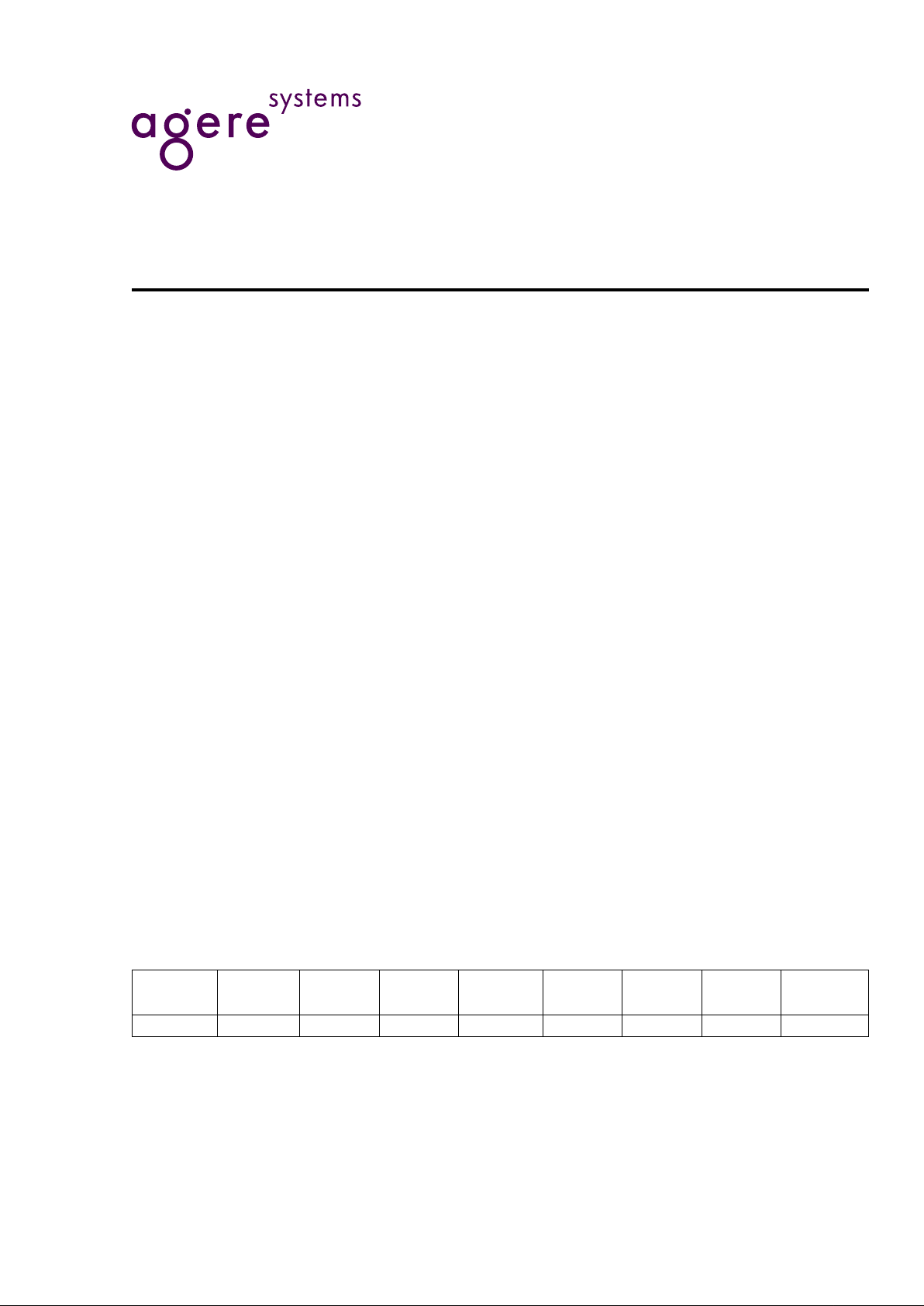
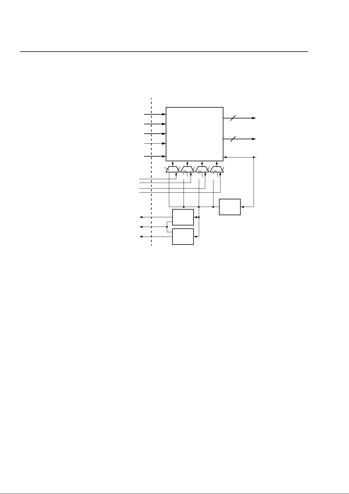
Figure 1 shows the O RLI10G block diagram.
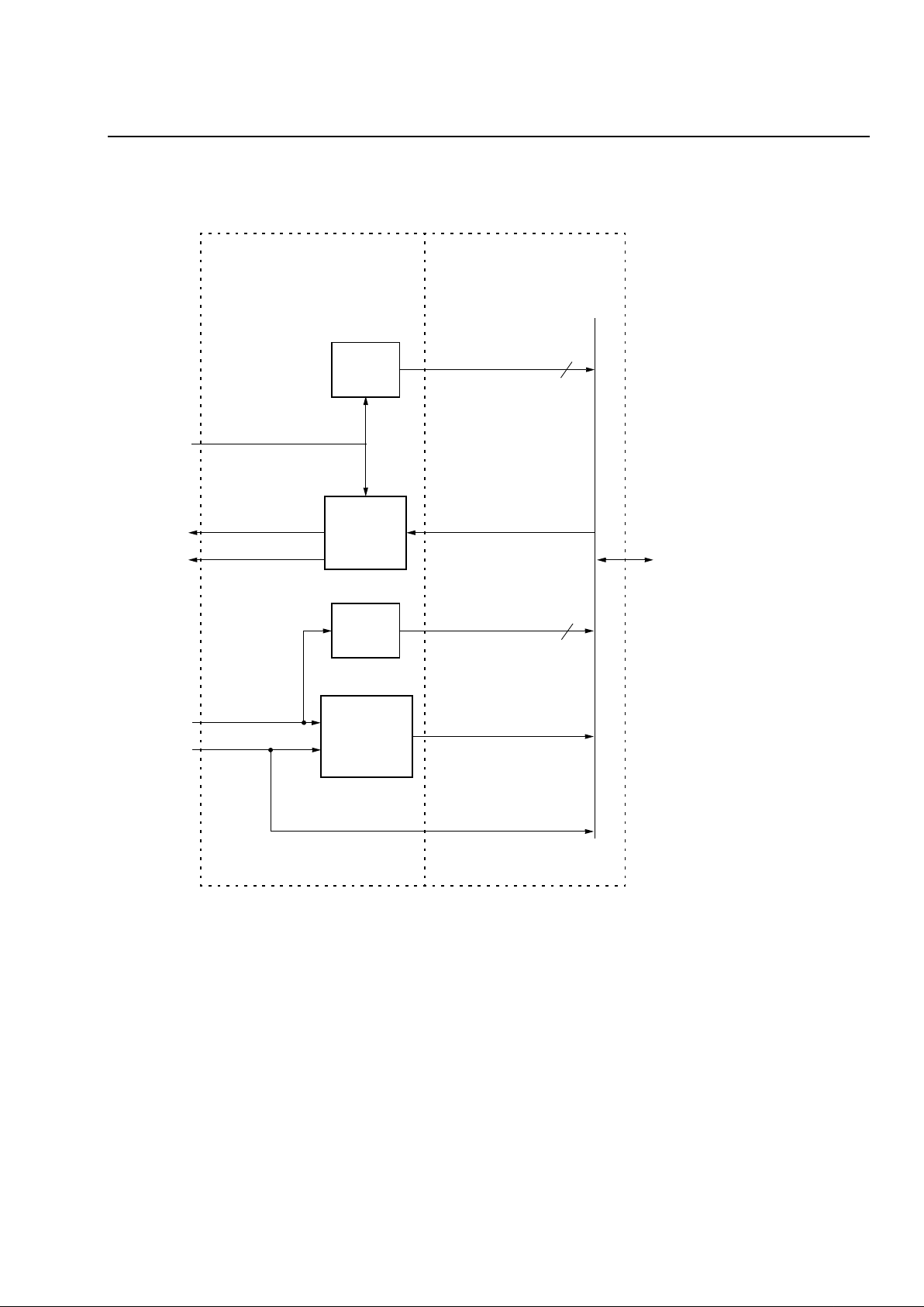
10G Mode
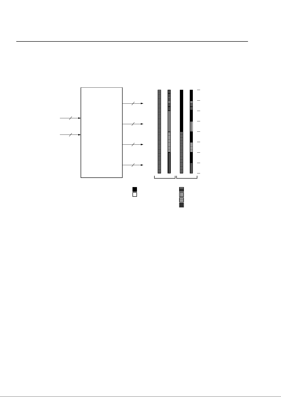
The ORLI10G can operate in one of two data modes:
10G mode or Quad 2.5G mode.
In 10G (or single-channel) mode, all 16 LVDS transmit
data outputs are assumed to be one data bus with one
LVDS clock provided off chip for the data. Likewise, all
16 LVDS receive data inputs are assumed to be one
data bus with one LVDS input clock provided for the
data.
Transmit Path
In 10G mode, the transmit data from the FPGA logic is
passed to the embedded core as a single 128- or 64-bit
bus. An off-chip transmit reference clock is divided
down in the core by 8 (for 128-bit to 16-bit MUX) or by
4 (for 64-bit to 16-bit MUX). All four transmit clock outputs are therefore synchronized.

1212 Agere Systems Inc.
Data Sheet
October 2001
10 Gbits/s, a nd 12.5 Gbits/s Line Interface FPSC
ORCA ORLI10G Quad 2.5 Gbits/s
ORLI10G Overview
(continued)
Receive Path
The 16-bit receive data is deMUXed in the embedded
core to a single 128-bit or 64-bit data bus and passed
to the FPGA logic. The lowest-order LVDS input clock
(rx_clk_in[0]) is used as the receive clock for all 16 data
bits (the other three LVDS input clock pairs should be
tied low). This clock is divided down in the core by 8
(for 16-bit to 128-bit deMUX) or by 4 (for 16-bit to 64-bit
deMUX) and passed to the FPGA logic with the data.
The ORLI10G supports transmit and receive data rates
up to 850 Mbits/s. Therefore, the total data rate for this
mode is 850 Mbits/s x 16 or 13.6 Gbits/s.
2.5G Mode
In 2.5G (or quad-channel) mode, the 16 LVDS transmit
data outputs are assumed to be four 4-bit data buses
with four LVDS clocks provided off chip for each data
bus. Likewise, the 16 LVDS receive data inputs are
assumed to be four independent 4-bit data buses with
four LVDS asynchronous input clocks provided for
each data bus.
Transmit Path
In 2.5G mode, the transmit data from the FPGA logic is
passed to the embedded core as four separate 32- or
16-bit buses. A separate clock for each of the four busses is also passed to the core. An off-chip transmit reference clock is divided down in the core by 8 (for each
32 to 8-bit MUX) or by 4 (for each 16 to 4 MUX). This
divided down clock is used to resynchronize the output
data and clocks. All four transmit clock outputs are
therefore synchronized.
Receive Path
Each of the four 4-bit receive data buses are deMUXed
in the embedded core to one of four independent 32- or
16-bit data buses and passed to the FPGA logic. The
four receive clock inputs are divided down in the core
by 8 (for each 4- to 32-bit deMUX) or by 4 (for each
4- to 16-bit deMUX), and each divided clock is passed
to the FPGA logic with its associated data bus. All four
data paths act as separate data interfaces that are
asynchronous to each other.
The ORLI10G supports transmit and receive data rates
up to 850 Mbits/s. Therefore, the total data rate each of
the quad channels is 850 Mbits/s x 4 or 3.4 Gbits/s.
Figure 2 shows a representation of the 10G and 2.5G
modes in both transmit and receive directions.
Agere Systems Inc. 13
Data Sheet
October 2001
10 Gbits/s, and 12.5 Gbits/s Line Interface FPSC
ORCA ORLI10G Quad 2.5 Gbits/s
ORLI10G Overview
(continued)
1018(F)
Figure 1.
ORCA
ORLI10G Block Diagram
EMBEDDED CORE FPGA LOGIC
(400K GATES)
TRANSMIT
PLLs
REFERENCE CLOCK
TRANSMIT DATA
16 x 622 OR
16 x 645 OR
16 x 667 OR
64:16 MUX
OR
128:16 MUX
TRANSMIT CLOCK
RECEIVE
PLLs
16:64 DEMUX
OR
16:128 DEMUX
RECEIVE DATA
16 x 622 OR
16 x 645 OR
16 x 667 OR
FOUR 2.5 Gbit RXCLKs
64-bit OR 128-bit
RXCLK
64-bit OR 128-bit
TXCLK
(167 MHz—78 MHz)
(167 MHz—78 MHz)
SYSTEM INTERFACE:
— POS-PHY 4
— XGMII
— 156 MHz PECL
(OC-48/STM-16
SONET/SDH)
— USER DEFINED
16 x 781 Mbits/s
16 x 781 Mbits/s
2
2
14 Agere Systems Inc.
Data Sheet
October 2001
10 Gbits/s, a nd 12.5 Gbits/s Line Interface FPSC
ORCA ORLI10G Quad 2.5 Gbits/s
ORLI10G Overview
(continued)
1335(F)
Figure 2. 10G (Single-Channel) and 2.5G (Quad-Channel) Modes
DATA
128 or 64
2.5G MODE
RECEIVE PATH
CORE
LVDS DATA
32 OR 16
FPGA
LVDS CLOCK
LVDS DATA
CORE FPGA
CLOCK
32 OR 16
4
DEMUX
FPGACORE
LVDS DATA
16
RX_CLK_IN[0]
RX_CLK_IN[31:1]
CLOCK
1
DATA
4
DATA
MUX
TRANSMIT PATH
10G MODE
DIV BY 8
OR
DIV BY 4
DIV BY 8
DIV BY 8
MUX
LVDS
16
TX_CLK_IN
CORE
128 OR 64
FPGA
DATA
UNUSED
REFERENCE
DATA
TRANSMIT PATH
MUX
MUX
MUX
32 OR 16
DATA
32 OR 16
DATA
32 OR 16
DATA
LVDS DATA
4
LVDS DATA
4
LVDS DATA
4
DIV BY 8
OR
DIV BY 4
1
1
LVDS CLOCK
LVDS DATA
CLOCK
32 OR 16
4
DEMUX
DATA
DIV BY 8
OR
DIV BY 4
1
1
LVDS CLOCK
LVDS DATA
CLOCK
32 OR 16
4
DEMUX
DATA
DIV BY 8
OR
DIV BY 4
1
1
LVDS CLOCK
LVDS DATA
CLOCK
32 OR 16
4
DEMUX
DATA
DIV BY 8
OR
DIV BY 4
1
1
RECEIVE PATH
DEMUX
CLOCK
DIV BY 4
TX[1:2]VCOP
2
DIV BY 4
TX_CLK_IN
REFERENCE
CLOCK
TX_CLK_OUT[3:0]
LVDS CLOCKS
TX_CLK8_IN[3:0]
4

Agere Systems Inc. 15
Data Sheet
October 2001
10 Gbits/s, and 12.5 Gbits/s Line Interface FPSC
ORCA ORLI10G Quad 2.5 Gbits/s
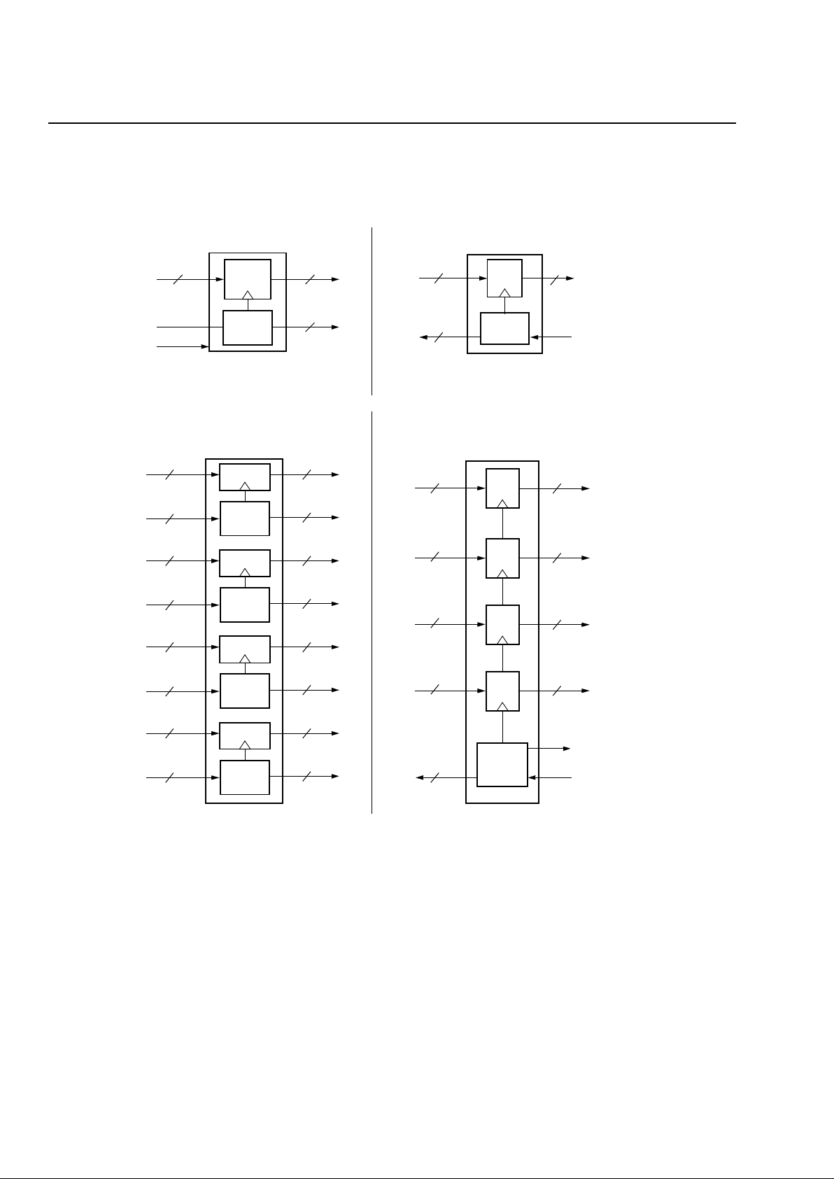
Receive Path Details
In the receive path, the ORLI10G embedded core can
be broken down into three sections: the high-speed line
interface, the demultiplexer, and the receive-side onboard PLLs. Note that both transmit and receive PLLs
are in addition to the four programmable PLLs (PPLLs)
in the FPGA portion of the ORLI10G.
Line Interface
In the receive path, 16-bit data and associated clocks
are inputs to the line interface. Typical data rates are
expected to range from 622 Mbits/s to 850 Mbits/s for
most applications. The 16-bit LVDS input data bus is
actually composed of four 4-bit data buses with one
clock for each 4-bit data bus. In the 10G mode, all four
input clocks are tied together internal to the device and
driven by the lowest-order input clock. In 2.5G mode,
the four clocks may be asynchronous to each other.
The ORLI10G uses LVDS (low-voltage differential signaling) drivers/receivers, which are intended to provide
point-to-point connection between the ORLI10G and
optical transceiver (MUX/deMUX) parts. The LVDS
inputs are hot-swap compatible and can connect to
other vendor’s LVDS I/O buffers. The LVDS inputs are
terminated with a 100 Ω resistor to improve performance.
The receive line interface on the ORLI10G can connect
to devices that are compliant to either the XSBI standard or the SFI-4 standard. The major difference for
these standards is that for XSBI (IEEE 802.3ae vers ion
2.1), the least significant bit [0] is received first after
deserialization by the external deMUX device, whereas
SFI-4 receives the most significant bit first. In some
cases, bits [15:0] on the ORLI10G should be connected to bits [0:15] on the device to which the
ORLI10G device interfaces to. An example of this is
the PCS IP core in the ORLI10G when the ORLI10G is
connected to an XSBI version 2.1 device.
It should be noted that IEEE 802.3ae version 3.1
swaps XSBI so that the most significant bit is received
first, thus requiring that bits [0:15] on the ORLI10G be
connected directly to bits [0:15] on the XSBI device.
DeMUX
The demultiplexer takes the high-speed line data and
clocks and converts the data and clock to rates appropriate for transfer to the FPGA logic. The demultiplexer
supports two modes of operation:
■
Divide-by-8
10G (or single channel): The demultiplexer converts
the incoming 16 bits of data at 622 Mbits/s to
850 Mbits/s into 128 bits at 78 Mbits/s to 106 Mbits/s.
The incoming clocks are divided by 8.
2.5G (or quad channel): The demultipl ex er conv er ts
the incoming four bits of data at 622 Mbits/s to
850 Mbits/s into 32 bits at 78 Mbits/s to 106 Mbits/s.
The associated clock is also divided by 8. This is
repeated four times with each 4-bit data/clock group
assumed to be asynchronous to the others.
■
Divide-by-4
10G (or single channel): The demultiplexer converts
the incoming 16 bits of data at 622 Mbits/s to
850 Mbits/s into 64 bits at 156 Mbits/s to 212 Mbits/s.
The incoming clocks are divided by 4.
2.5G (or quad channel): The demultipl ex er conv er ts
the incoming 4 bits of data at 622 Mbits/s to
850 Mbits/s into 16 bits at 156 Mbits/s to 212 Mbits/s.
The associated clock is also divided by 4. This is
repeated four times with each 4-bit data/clock group
assumed to be asynchronous to the others.
Onboard Receive PLLs
The function of the onboard PLLs is to align the system
data with the line data which will be at a slightly higher
rate owing to the addition of the overhead bits. There
are two PLLs on the receive path. The input to the first
PLL, RX1_PLL (see Figure 3), is the divided down lowest-order clock from the demultiplexer. The RX1_PLL
generates a clock with a user-defined frequency ratio
of M/N to the divided clock. This clock would generally
be used to compensate for different data rates due to
overhead bits. M and N can independently be set from
1 to 8.
The RX2_PLL also takes its input from the divided
down clock and is used to provide a balanced divided
clock across the FPGA-embedded core interface.
Both PLLs have delay loops which compensate for
routing delays to the embedded core/FPGA logic interface for minimum clock skew.
In addition, the user can specify an additional skew on
each clock in increments of 1/8 the clock period.
The selection of the deMUX width (and corresponding
clock division value), the RX1_PLL M and N values,
and the additional skew for RX1_PLL and RX2_PLL
are specified by the user in a GUI interface provided in
the ORLI10G design kit.
A detailed block diagram of the receive path in shown
in Figure 3.
16 Agere Systems Inc.
Data Sheet
October 2001
10 Gbits/s, a nd 12.5 Gbits/s Line Interface FPSC
ORCA ORLI10G Quad 2.5 Gbits/s
Receive Path Details
(continued)
1333(F)
Figure 3. ORLI10G Embedded Core Receive Path Diagram
128 TO 16 MUX
OR
64 TO 16 MUX
DATA
RX_DAT_IN
16
CLOCK
RX_CLK_IN
4
FPGA LOGIC
DIVIDE BY 8 MODE
RX_DAT_OUT[127:96]
RX_DAT_OUT[95:64]
RX_DAT_OUT[63:32]
RX_DAT_OUT[31:0]
OR
RX_ENB_OUT[3:0]
DIVIDE BY 4 MODE
RX_DAT_OUT[111:96]
RX_DAT_OUT[79:64]
RX_DAT_OUT[47:32]
RX_DAT_OUT[15:0]
RX_CLK8_OUT[0]
RX_CLK8_OUT[1]
RX_CLK8_OUT[2]
RX_CLK8_OUT[3]
DIV BY 8
OR
DIV BY 4
ORLI10G CORE
RX1_PLL
(M/N)
RX2_PLL
(X1)
RX1_VCOP (X M/N CLOCK)
RX_LOCK
RX2_VCOP (X 1 CLOCK)
DIV BY 8
OR
DIV BY 4
DIV BY 8
OR
DIV BY 4
DIV BY 8
OR
DIV BY 4
RX_ENB_OUT[3:0]
RX1_VCO
RX2_VCO

Agere Systems Inc. 17
Data Sheet
October 2001
10 Gbits/s, and 12.5 Gbits/s Line Interface FPSC
ORCA ORLI10G Quad 2.5 Gbits/s
Transmit Path Details
In the transmit path, the ORLI10G embedded core can
be broken down into three sections: the multiplexer, the
transmit side onboard PLLs, and the high-speed line
interface. Note that both transmit and receive PLLs are
in addition to the four programmable PLLs (PPLLs) in
the FPGA portion of the ORLI10G.
MUX
The multiplexer takes data from the FPGA logic and
multiplexes the data to rates for transfer by the highspeed line interface. The multiplexer supports two
modes of operation:
■
Multiplex-by-8
The multiplexer converts the incoming 128 bits of data
at 78 Mbits/s to 106 Mbits/s into 16 bits at 622 Mbits/s
to 850 Mbits/s. The incoming transmit reference clock
is divided by 8.
■
Multiplex-by-4
10G (or single channel): The multiplexer converts the
incoming 64 bits of data at 156 Mbits/s to 212 Mbits/s
into 16 bits at 622 Mbits to 850 Mbits/s. The transmit
reference clock is divided by 4.
Onboard Transmit PLLs
The function of the onboard PLLs is to align the system
data with the line data which will be at a slightly higher
rate owing to the addition of the overhead bits. There
are two PLLs on the transmit path. The input to the first
PLL, TX1_PLL (see Figure 4), is the divided down
transmit reference clock from the multiplexer. The
TX1_PLL generates a clock with a user-defined frequency ratio of M/N to the divided clock. This clock
would generally be used to compensate for different
data rates due to overhead bits. M and N can be independently set from 1 to 8.
The TX2_PLL also takes its input reference from the
divided down reference clock and is used to provide a
balanced divided clock across the FPGA-embedded
core interface.
Both PLLs have delay loops which compensate for
routing delays to the embedded core/FPGA logic interface for minimum clock skew.
In addition, the user can specify an additional skew on
each clock in increments of 1/8 the clock period.
The selection of the MUX width (and corresponding
clock division value), the TX1_PLL M and N values,
and the additional skew for TX1_PLL and TX2_PLL are
specified by the user in a GUI interface provided in the
ORLI10G design kit.
A detailed block diagram of the transmit path in shown
in Figure 4. In 10 Gbit mode, either TX1_VCOP or
TX2_VCOP must be used to clock TX_DAT_IN[127:0]
that is transmitted to the embedded block. These PLLs
can also be bypassed, where the divided transmit reference clock is sent directly to the FPGA. In 2.5 Gbit
mode, TX_CLK8_IN[3:0] is used to clock data transmitted to the embedded block.
Line Interface
In the transmit path, 16-bit data and associated clocks
are outputs from the line interface. Typical data rates
are expected to range from 622 Mbits/s to 850 Mbits/s
for most applications. The 16-bit LV DS output data bus
is actually composed of four 4-bit data buses with one
clock for each 4-bit data bus. On the transmit side,
these clocks will all be synchronized. The ORLI10G
uses LVDS (low-voltage differential signaling)
drivers/receivers, which are intended to provide pointto-point connection between the ORLI10G and optical
transceiver (MUX/deMUX) parts. The LVDS drivers are
hot-swap compatible and can connect to other
vendor’s LVDS I/O buffers. The LVDS drivers are
terminated with a 100 Ω resistor to improve
performance.
The transmit line interface on the ORLI10G can connect to devices that are compliant to either the XSBI
standard or the SFI-4 standard. The major difference
for these standards is that for XSBI, the least significant bit [0] is transferred first after serialization by the
external MUX device, whereas SFI-4 transmits the
most significant bit first. In some cases, bits [15:0] on
the ORLI10G should be connect to bits [0:15] on the
device to which the ORLI10G device interfaces to. An
example of this is the PCS IP core in the ORLI10G
when the ORLI10G is connected to an XSBI version
2.1 device.
It should be noted that IEEE 802.3ae version 3.1
swaps XSBI so that the most significant bit is transferred first, thus requiring that bits [0:15] on the
ORLI10G be connected directly to bits [0:15] on the
XSBI device.
18 Agere Systems Inc.
Data Sheet
October 2001
10 Gbits/s, a nd 12.5 Gbits/s Line Interface FPSC
ORCA ORLI10G Quad 2.5 Gbits/s
Transmit Path Details
(continued)
1332(F)
Figure 4. ORLI10G Embedded Core Trans mit Path Diagram
128 TO 16 MUX
OR
64 TO 16 MUX
DATA
TX_DAT_OUT
16
CLOCK
TX_CLK8_OUT
4
TRANSMIT REFERENCE
CLOCK
FPGA LOGIC
DIVIDE BY 8 MODE
TX_DAT_IN[127:96]
TX_DAT_IN[95:64]
TX_DAT_IN[63:32]
TX_DAT_IN[31:0]
OR
TX_ENB_IN[3:0]
DIVIDE BY 4 MODE
TX_DAT_IN[111:96]
TX_DAT_IN[79:64]
TX_DAT_IN[47:32]
TX_DAT_IN[15:0]
10G
2.5G
TX_CLK8_IN[0]
TX_CLK8_IN[1]
TX_CLK8_IN[2]
TX_CLK8_IN[3]
DIV BY 8
OR
DIV BY 4
TX_CLK_IN
ORLI10G CORE
TX1_PLL
(M/N)
TX2_PLL
(X1)
TX1_VCOP (X M/N CLOCK)
TX_LOCK
TX2_VCOP (X 1 CLOCK)
2.5G 2.5G 2.5G
10G 10G 10G
TX_ENB_IN[3:0]
TX1_VCO
TX2_VCO

Agere Systems Inc. 19
Data Sheet
October 2001
10 Gbits/s, and 12.5 Gbits/s Line Interface FPSC
ORCA ORLI10G Quad 2.5 Gbits/s
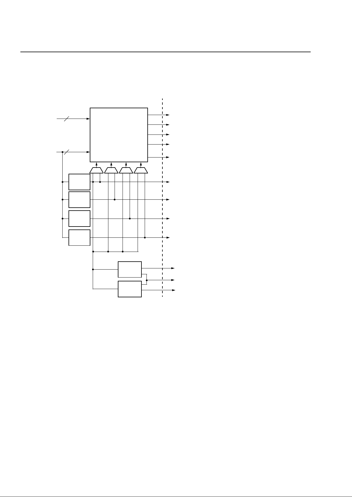
ORLI10G Demultiplexer (Rx) Detail
The demultiplexer module converts the incoming
16 bits of data at 622 MHz/850 MHz into 128 bits of
data at 78 MHz/106 MHz or 64 bits of data at
156 MHz/212 MHz and sends it to the FPGA logic. It
has been implemented in two stages: the first stage
converts each incoming bit into a byte stream and the
second stage bit interleaves these bytes into
128/64 bits, depending upon the mode of operation.
The low-speed clocks are generated by this block.
These clocks are then driven back to this block from
the low-speed clock tree network. Functionally, the
demultiplexer architecture consists of three blocks: the
serial to parallel conversion, the counters, and the
interleaving.
The first stage of the line interface module (demultiplexer) converts each incoming bit of data into a byte
stream on a divided-by-8 clock. The data is first registered on the rising edge of the clock input. The clock
dividers also runs parallel to data shift (serial to parallel), on the rising edge of the input clock. An enable is
created when a complete byte is taken in. This enable
signal is used to register the serial-to-parallel converted data at the high-speed input clock. This ensures
that the data can be safely transferred to the low-speed
clock. This data is then transferred to the divided clock,
allowing a timing margin of approximately half the
divided clock period.
The high-speed demultiplexer converts the incoming
data as blocks of bytes. The byte boundaries of incoming data are unknown and are irrelevant to this module.
This data is then interleaved to the 128/64 bits of output data, depending on the mode of operation (divideby-4/divide-by-8). In 10G mode, the output data is
assigned the retimed 128/64 bits of data from the first
stage of line interface registered at the input clock [0].
In 2.5G mode, the output data is assigned four concatenated 32/16 bits of data from the first stage of line
interface registered at input clocks [0 to 3]. The interleaving is done at bit level because the serial-to-parallel converter operates on bits of incoming data. In 10G
mode, it is assumed that all the incoming 16 bits of
data are sy nchronized to the input clock [0]. This block
also generates the clock enables used by the output
line interface (multiplexer) module for registering the
data on the high-speed clock. These enables along
with the enables from other clocks are selected through
the high-speed clock MUX for the output line interface
block.
20 Agere Systems Inc.
Data Sheet
October 2001
10 Gbits/s, a nd 12.5 Gbits/s Line Interface FPSC
ORCA ORLI10G Quad 2.5 Gbits/s
ORLI10G Demultiplexer (Rx) Detail
(continued)
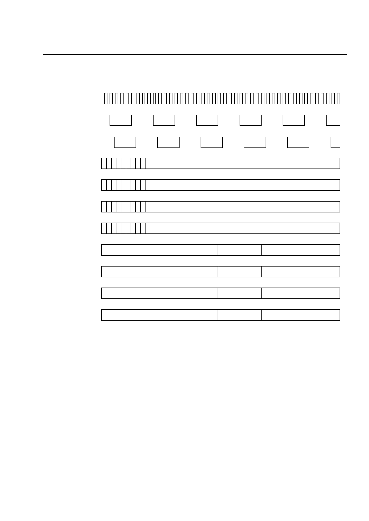
Figure 5 shows the valid data output bits from the demultiplexer in each of the four modes (divide-by-8, 10G and
2.5G modes, and divide-by-4, 10G and 2.5G modes). Figure 6—Figure 9 show the demultiplexer input data and
clock waveforms and output clock, enable, and data waveforms for all four modes.
1338(F)
Figure 5. Demultiplexer Output Data Structure
4x4 TO 32 DEMUX
OR
4x4 TO 16 DEMUX
RX_DAT_OUT
16 OR 32
RX_DAT_OUT
16 OR 32
RX_DAT_OUT
16 OR 32
RX_DAT_OUT
16 OR 32
RX_DAT_IN
16
RX_CLK_IN
4
128
112
96
80
64
48
32
16
0
10G 2.5G
÷
8 MODE
÷
4 MODE
2.5G10G
UNDEFINED
SINGLE CHANNEL
CHANNEL 3
CHANNEL 2
CHANNEL 1
CHANNEL 0
Agere Systems Inc. 21
Data Sheet
October 2001
10 Gbits/s, and 12.5 Gbits/s Line Interface FPSC
ORCA ORLI10G Quad 2.5 Gbits/s
ORLI10G Demultiplexer (Rx) Detail
(continued)
1340(F)
Figure 6. Demultiplexer Serial-to-Parallel Conversion—Divide by 8, 10G Mode
(RX_ENB8_OUT[1:3] = 0)
0048C1908 0
0159D3B2A 0
026AE5D4C 0
037BF7F6E 0
00000000 01234567 0
00000000 89ABCDEF 0
00000000 13579BDF 0
00000000 02468ACE 0
RX_CLK_IN0
RX_CLK8_OUT0
(RX_CLK8_OUT[1:3] = 0)
RX_DAT_IN
[15:12]
RX_ENB8_OUT0
RX_DAT_IN
[11:8]
RX_DAT_IN
[7:4]
RX_DAT_IN
[3:0]
RX_DAT_OUT
[127:96]
RX_DAT_OUT
[95:64]
RX_DAT_OUT
[63:32]
RX_DAT_OUT
[31:0]
22 Agere Systems Inc.
Data Sheet
October 2001
10 Gbits/s, a nd 12.5 Gbits/s Line Interface FPSC
ORCA ORLI10G Quad 2.5 Gbits/s
ORLI10G Demultiplexer (Rx) Detail
(continued)
1341(F)
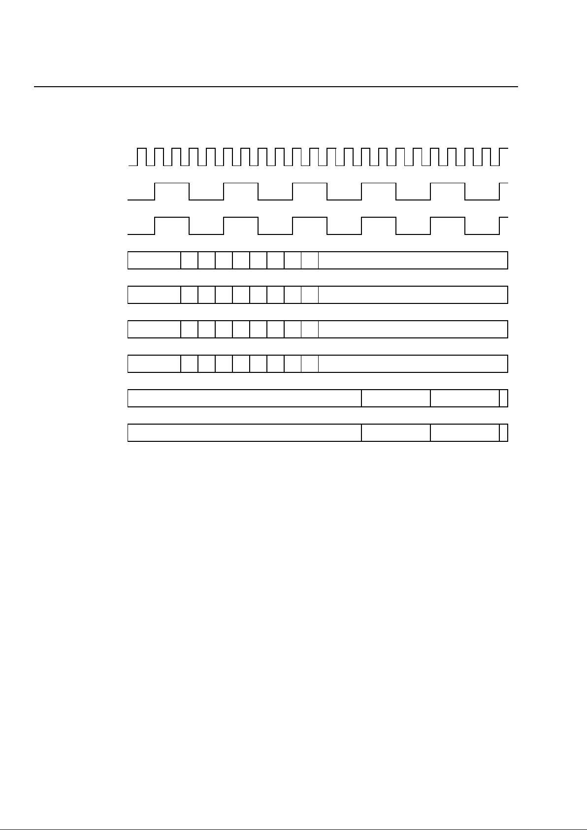
Figure 7. Demultiplexer Serial-to-Parallel Conversion—Divide by 4, 10G Mode
0 048C19080
00000000 01234567 0
(RX_ENB8_OUT[1:3] = 0)
RX_CLK_IN0
RX_CLK8_OUT0
(RX_CLK8_OUT[1:3] = 0)
RX_DAT_IN
[15:12]
RX_ENB8_OUT0
RX_DAT_IN
[11:8]
RX_DAT_IN
[7:4]
RX_DAT_IN
[3:0]
RX_DAT_OUT
[63:32]
RX_DAT_OUT
[31:0]
0159D3B2A0
026AE5D4C0
037BF7F6E0
13579BDF
00000000 89ABCDEF 002468ACE
 Loading...