

AGERE OR4E6-1BA352, OR4E6-2BM680, OR4E10-1BM680, OR4E2-1BA352, OR4E2-2BC352 Datasheet
...
Preliminary Data Sheet
December 2000
ORCA®
Series 4
Field-Programmable Gate Arrays
Programmable Features
■
High-performance platform design.
— 0.13 µm seven-level metal technology.
— Internal performance of >250 MHz
(four logic levels).
— I/O performance of >416 M H z for all user I/Os.
— Over 1.5 million usable system gates.
— Meets multiple I/O interface standards.
— 1.5 V operation (30% l e ss p o w er t han 1 .8 V op er -
ation) translates to greater performance.
— Embedded block RAM (EBR) for onboard stor-
age and buffer needs.
— Built-in system component s i n cl udi ng a n i nt ernal
system bus, eight PLLs, and microprocess or
interface.
■
Traditional I/O selections.
— LVTTL and LVCMOS (3.3 V, 2.5 V, and 1.8 V)
I/Os.
— Per pin-selectable I/O clamping diodes provide
3.3 V PCI compliance.
— Individually programmable drive capabilit y.
24 mA sink/12 mA sourc e, 12 mA si nk /6 mA
source, or 6 mA sink/3 mA source.
— Two slew rates supported (fast and slew-limited).
— Fast-capture input latch and input flip-flop (FF)/
latch for reduced input setup time and zero ho ld
time.
— Fast open-drain drive capability.
— Capability to register 3-state enable signal.
— Off-chip clock drive capability.
— Two-input function generator in output path.
■
New programmable high-speed I/O.
— Single-ended: GTL , GTL+, PECL, SSTL3/2
(class I & II), HSTL (Class I, III, IV), zero-bus
turn-around (
ZBT*
), and double data rate (DDR).
— Double-ended: LDVS, bused-LVDS, LVPECL.
— Customer defined: Ability to substitute arbitrary
standard-cell I/O to meet fast moving standards.
■
New capability to (de)multiplex I/O signals.
— New DDR on both input and output a t r ates up to
311 MHz (622 MHz effective rate).
— Used to implement emerging
RapidIO
†
back-
plane interface specification.
— New 2x and 4x downlink and uplink capability per
I/O (i.e., 104 MHz internal to 416 MHz I/O).
■
Enhanced twin-quad programmable function unit
(PFU).
— Eight 16-bit look-up tables (LUTs ) per PFU.
— Nine user registers pe r PF U, one following each
LUT and organized to allow two nibbles to act
independently, plus one extra for arithmetic
carry/borrow op eratio ns.
*
ZBT
is a trademark of Integrated Device Technologies Inc.
†
RapidIO
is a trademark of Motorola, Inc.
Table 1.
ORCA
Series 4—Available FPGA Logic
† The usable gate counts range from a logic-only gate count to a gate count assuming 20% of the PFUs/SLICs being used as RAMs. The
logic-only gate count includes each PFU/SLIC (counted as 108 gates/PFU), including 12 gates per LUT/FF pair (eight per PFU), and
12 gates per SLIC/FF pair (one per PFU). Each of the four PIO groups are counted as 16 gates (three FFs, fast-capture latch, output logic,
CLK, and I/O buffers). PFUs used as RAM are counted at four gates per bit, with each PFU capable of implementing a 32 x 4 RAM (or
512 gates) per PFU. Embedded block RAM (EBR) is counted as four gates per bit plus each block has an additional 25k gates. 7k gates
are used for each PLL and 50k gates for the embedded system bus and microprocessor interface logic. Both the EBR and PLLs are conservatively utilized in the gate count calculations.
Note: Devices are not pinout compatible with
ORCA
Series 2/3.
Device Columns Rows PFUs User I/O LUTs EBR
Blocks
EBR Bits (k)
Usable†
Gates (k)
OR4E2 26 24 624 400 4992 8 74 260—470
OR4E4 36 36 1296 576 10368 12 111 400—720
OR4E6 46 44 2024 720 16,192 16 148 530—970
OR4E10 60 56 3360 928 26,880 20 185 740—1350
OR4E14 70 66 4620 1088 36,960 24 222 930—1700

Table of Contents
Contents Page Contents Page
2 Lucent Technologies Inc.
Preliminary Data Sheet
December 2000
ORCA
Series 4 FPGAs
Programmable Features............................................. 1
System Features ................................... ....... ...... ....... ..4
Product Description .....................................................6
Architecture Overview .............................................6
Programmable Logic Cells ..........................................7
Programmable Function Unit...................................8
Look-Up Table Operating Modes ..........................11
Supplemental Logic and Interconnect Cell ............21
PLC Latches/Flip-Flops .........................................25
Embedded Block RAM ..............................................27
EBR Features........................................................27
Routing Resources ...................................................31
Clock Distribution Network ........................................31
Primary Clock Nets................................................31
Secondary Clock and Control Nets .......................31
Edge Clock Nets....................................................31
Programmable Input/Output Cells.............................31
Programmable I/O .................................................31
Inputs.....................................................................34
Special Function Blocks ............................................38
Microprocessor Interface (MPI).................................48
Embedded System Bus (ESB) ..................................49
Phase-Locked Loops.................................................52
FPGA States of Operation.........................................55
Initialization............................................................56
Configuration .........................................................56
Start-Up .................................................................56
Reconfiguration .....................................................60
Partial Reconfiguration..........................................60
Other Configuration Options..................................60
Bit Stream Error Checking.....................................62
FPGA Configuration Modes.......................................62
Master Parallel Mode.............................................63
Master Serial Mode ...............................................64
Asynchronous Peripheral Mode ............................65
Microprocessor Interface Mode .............................66
Slave Serial Mode .................................................70
Slave Parallel Mode...............................................70
Daisy Chaining ......................................................71
Daisy-Chaining with Boundary Scan .....................72
Absolute Maximum Ratings.......................................72
Recommended Operating Conditions .......... ...... .......73
Electrical Characteristics...........................................73
Pin Information ..........................................................75
Pin Descriptions.....................................................75
Package Compatibility ...........................................78
Package Thermal Characteristics Summary ...........118
Θ
JA
......................................................................118
ψ
JC
......................................................................118
Θ
JC
......................................................................118
Θ
JB
......................................................................118
Package Thermal Characteristics............................119
Package Coplanarity ...............................................119
Package Parasitics..................................................119
Package Outline Diagrams......................................120
Terms and Definitions..........................................120
Package Outline Drawings......................................121
352-Pin PBGA .....................................................121
432-Pin EBGA .....................................................122
680-Pin PBGAM ..................................................123
Ordering Information................................................124
Figure Page
Figure 1. Series 4 Top-Level Diagram ........................7
Figure 2. PFU Ports.....................................................9
Figure 3. Simplified PFU Diagram.............................10
Figure 4. Simplified F4 and F5 Logic Modes.............12
Figure 5. Simplified F6 Logic Modes .........................13
Figure 6. MUX 4 x 1...................................................13
Figure 7. MUX 8 x 1...................................................14
Figure 8. Softwired LUT Topology Examples.............15
Figure 9. Ripple Mode ...............................................16
Figure 10. Counter Submode....................................17
Figure 11. Multiplier Submode...................................18
Figure 12. Memory Mode ..........................................19
Figure 13. Memory Mode Expansion
Example—128 x 8 RAM ........................................21
Figure 14. SLIC All Modes Diagram..........................22
Figure 15. Buffer Mode..............................................23
Figure 16. Buffer-Buffer-Decoder Mode ....................23
Figure 17. Buffer-Decoder-Buffer Mode ....................24
Figure 18. Buffer-Decoder-Decoder Mode ................24
Figure 19. Decoder Mode..........................................25
Figure 20. Latch/FF Set/Reset Configurations ..........26
Figure 21. EBR Read and Write Cycles
with Write Through ................................................29
Figure 22. Series 4 PIO Image from
ORCA Foundry.................. ...... ..............................33
Figure 23. ORCA High-Speed I/O Banks ..................36
Figure 24. PIO Shift Register.....................................38
Figure 25. Printed-Circuit Board with Boundary-
Scan Circuitry ........................................................39
Figure 26. Boundary-Scan Interface..........................40
Figure 27. ORCA Series Boundary-Scan
Circuitry Functional Diagram .................................43
Figure 28. TAP Controller State T ransition
Diagram.................................................................44
Figure 29. Boundary-Scan Cell .................................45
Figure 30. Instruction Regist er Scan Timing
Diagram.................................................................46
Figure 31. PLL_VF External Requirements...............53
Figure 32. PLL Naming Scheme ...............................54

Lucent Technologies Inc. 3
Preliminary Data Sheet
December 2000
ORCA Series 4 FPGAs
Contents Page Contents Page
Table of Contents
(continued)
Figure 33. FPGA States of Operation .......................55
Figure 34. Initialization/Configuration/Start-Up
Waveforms............................................................. 57
Figure 35. Start-Up Waveforms.................................59
Figure 36. Serial Configuration Data
Format—Autoincrement Mode ..............................60
Figure 37. Serial Configuration Data
Format—Expl ic it Mod e......... ....... ...... ....... ...... ....... 60
Figure 38. Master Parallel
Configuration Schematic ....................................... 63
Figure 39. Master Serial Configuration Schematic.... 65
Figure 40. Asynchronous Peripheral Configuration...66
Figure 41. PowerPC/MPI Configuration Schematic...67
Figure 42. Configuration Through MPI......................68
Figure 43. Readback Through MPI ...........................69
Figure 44. Slave Serial Configuration Schematic...... 70
Figure 45. Slave Parallel Configuration Schematic ...71
Figure 46. Daisy-Chain Configuration Schematic .....72
Figure 47. Package Parasitics................................. 120
Table Page
Table 1. ORCA Series 4—Available FPGA Logic.......1
Table 2. System Performance ....................................5
Table 3. Look-Up Table Operating Modes ................11
Table 4. Control Input Functionality..........................11
Table 5. Ripple Mode Equality Comparator
Functions and Outputs .......................................... 18
Table 6. SLIC Modes................................................22
Table 7. Configuration RAM Controlled Latch/
Flip-Flop Operation................................................25
Table 8. ORCA Series 4— Available
Embedded Block RAM .......................................... 27
Table 9. RAM Signals............................................... 28
Table 10. FIFO Signals ............................................29
Table 11. Constant Multiplier Signals .......................30
Table 12. 8 x 8 Multiplier Signals..............................30
Table 13. CAM Signals .............................................30
Table 14. Series 4 Programmable I/O Standards..... 32
Table 15. PIO Options ..............................................35
Table 16. PIO Register Control Signals....................35
Table 17. PIO Logic Options..................................... 36
Table 18. Compatible Mixed I/O Standards..............36
Table 19. LVDS I/O Specifications...........................37
Table 20. LVDS Termination Pin ............................. 37
Table 21. Dedicated Temperature Sensing..............39
Table 22. Boundary-Scan Instructions ..................... 40
Table 23. Series 4E Boundary-Scan
Vendor-ID Codes...................................................41
Table 24. TAP Controller Input/Outputs................... 43
Table 25. Readback Options .................................... 46
Table 26. MPC 860 to ORCA MPI Interconnection .. 48
Table 27. Embedded System Bus/MPI Registers..... 50
Table 28. Interrupt Register Space Assignments..... 50
Table 29. Status Register Space Assignments ........ 51
Table 30. Command Register Space Assignments.. 51
Table 31. PPLL Specifications.................................. 52
Table 32. DPLL DS-1/E-1 Specifications..................53
Table 33. Dedicated Pin Per Package...................... 53
Table 34. STS-3/STM-1 DPLL Specifications........... 54
Table 35. Phase-Lock Loops Index .......................... 54
Table 36A. Configuration Frame Format
and Contents......................................................... 61
Table 36B. Configuration Frame Format
and Contents for Embedded Block RAM...............61
Table 37. Configuration Frame Size ......................... 62
Table 38. Configuration Modes................................. 63
Table 39. Absolute Maximum Ratings...................... 73
Table 40. Recommended Operating Conditions....... 73
Table 41. Electrical Characteristics .......................... 73
Table 42. Pin Descriptions........................................75
Table 43. ORCA I/Os Summary ............................... 78
Table 44. 352-Pin PBGA Pinout ...............................79
Table 45. 432-Pin EBGA .......................................... 89
Table 46. 680-Pin PBGAM Pinout ............................99
Table 47. ORCA Series 4 FPGAs Plastic
Package Thermal Guidelines .............................. 119
Table 48. ORCA Series 4 FPGAs
Package Parasitics ..............................................119
Table 49. Series 4 Package Matrix
(Speed Grades).............................. ...... ....... ...... .. 124
Table 50. Package Options..................................... 124

4 Lucent Technologies Inc.
Preliminary Data Sheet
December 2000
ORCA Series 4 FPGAs
Programmable Features
(continued)
— New register control in each PFU has two inde-
pendent programmable clocks, clock enables,
local set/reset, and data selects.
— New LUT structure allows flexible combinations of
LUT4, LUT5, new LUT6, 4-to-1 MUX, new
8-to-1 MUX, and ripple mode arithmetic functions
in the same PFU.
— 32 x 4 RAM per PFU, configurable as single- or
dual-port. Create large, fast RAM/ROM blocks
(128 x 8 in only eight PFUs) using the supplemental logic and interconnect cell (SLIC) decoders as
bank drivers.
— Softwired LUTs (SWL) allow fast cascading of up
to three levels of LUT logic in a single PFU
through fast internal routing which reduces routing
congestion and improves speed.
— Flexible fast access to PFU inputs from routing.
— Fast-carry logic and routing to all four adjacent
PFUs for nibble-, bytewide, or longer arithmetic
functions, with the option to register the PFU
carry-out.
■
Abundant high-speed buffered and nonbuffered routing resources provide 2x average speed improvements over previous architectures.
■
Hierarchical routing optimized for both local and global routing with dedicated routing resources. This
results in faster routing times with predictable and
efficient performance.
■
SLIC provides eight 3-statable buffers, up to 10-bit
decoder, and PAL
1
-like and-or-invert (AOI) in each
programmable logic cell.
■
New 200 MHz embedded quad-port RAM blocks, two
read ports, two write ports, and two sets of byte lane
enables. Each embedded RAM block can be configured as:
— One 512 x 18 (quad-port, two read/two write) with
optional built-in arbitration.
— One 256 x 36 (dual-port, one read/one write).
— One 1K x 9 (dual-port, one read/one write).
— Two 512 x 9 (dual-port, one read/one write for
each).
— Two RAMs with arbitrary number of words whose
sum is 512 or less by 18 (dual-port, one read/one
write).
— Supports joining of RAM blocks.
— Two 16 x 8-bit content addressable memory
(CAM) support.
— FIFO 512 x 18, 256 x 36, 1K x 9 or dual 512 x 9.
— Constant multiply (8 x 16 or 16 x 8).
— Dual-variable multiply (8 x 8).
■
Built-in testability.
— Full boundary- sc an (IEEE
2
1149.1 and Draft
1149.2 joint test access group (JTAG)).
— Programming and readback through boundary-
scan port compliant to IEEE Draft 1532:D1.7.
— TS_ALL testability function to 3-state all I/O pins.
— New temperature-sensing diode used to deter-
mine device junction temperature.
System Features
■
PCI local bus compliant.
■
Improved PowerPC3 860 and PowerPC II high-speed
(66 MHz) synchronous MPI interface can be used for
configuration, readback, device control, and device
status, as well as for a general-purpose interface to
the FPGA logic, RAMs, and embedded standard-cell
blocks. Glueless interface to synchronous PowerPC
processors with user-configurable address space
provided.
■
New embedded AMBA4 specification 2.0 AHB system bus (ARM
4
processor) facilitates communication
among the microprocessor interface, configuration
logic, EBR, FPGA logic, and embedded standard-cell
blocks. Embedded 32-bit internal system bus plus
4-bit parity interconn ec ts FPG A log ic, microp ro ce ssor interface (MPI), embedded RAM blocks, and
embedded standard-cell blocks with 100 MHz bus
performance. Included are built-in system regis te rs
that act as the control and status center for the
device.
■
New network phase-locked loops (PLLs) meet ITU-T
G.811 specifications and provide clock conditioning
for DS-1/E-1 and STS-3/STM-1 applications.
■
Flexible general-purpose programmable PLLs offer
clock multiply (up to 8x), divide (down to 1/8x), phase
shift, delay compensation, and duty cycle adjustment
combined. Improved built-in clock management with
programmable phase-locked loops (PPLLs) provide
optimum clock modification and conditioning for
phase, frequency , and duty cycle from 20 MHz up to
420 MHz. Each PPLL provides two separate clock
outputs.
1. PA L is a trademark of Advanced Micro Devices, Inc.
2. IEEE a is registered trademark of The Institute of Electrical and
Electronics Engineers, Inc.
3. PowerPC is a registered trademark of International Business
Machines, Corporation.
4. AMBA and ARM are trademarks of ARM Limited.

Lucent Technologies Inc. 5
Preliminary Data Sheet
December 2000
ORCA Series 4 FPGAs
System Features
(continued)
■
Variable-size bused readback of configuration data capability with the built-in MPI and system bus.
■
Internal, 3-state, bidirectional buses with simple control provided by the SLIC.
■
Meets universal test and operations PHY interface for ATM (UTOPIA) Levels 1, 2, and 3. Also meets proposed
specifications for UTOPIA Level 4 for 10 Gbits/s interfaces.
■
New clock routing structures for global and local clocking significantly increases speed and reduces skew
(<200 ps for OR4E4).
■
New local clock routing structures allow creation of localized clock trees anywhere on the device.
■
New DDR, QDR, and ZBT memory interfaces support the latest high-speed memory interfaces.
■
New 2x/4x uplink and downlink I/O shift registers capabilities interface high-speed external I/Os to reduced internal logic speed.
■
ORCA Foundry 2000 development system software. Supported by industry-standard CAE tools for design entry,
synthesis, simulation, and timing analysis.
Table 2. System Performance
1. Implemented using 8 x 1 multiplier mode (unpipelined), register-to-register, two 8-bit inputs, one 16-bit output.
2. Implemented using two 32 x 4 RAMs and one 12-bit adder, one 8-bit input, one fixed operand, one 16-bit output.
3. Implemented using 8 x 1 multiplier mode (fully pipelined), two 8-bit inputs, one 16-bit output (seven of 15 PFUs
contain only pipelining registers).
4. Implemented using 32 x 4 RAM mode with read data on 3-state buffer to bidirectional read/write bus.
5. Implemented using 32 x 4 dual-port RAM mode.
6. Implemented in one partially occupied SLIC, with decoded output setup to CE in the same PLC.
7. Implemented in five partially occupied SLICs.
Function No. PFUs 2 Unit
16-bit loadable up/down counter 2 282 MHz
16-bit accumulator 2 282 MHz
8 x 8 Parallel Multiplier
Multiplier mode, unpipelined
1
11.5 72 MHz
ROM mode, unpipelined
2
8175MHz
Multiplier mode, pipelined
3
15 197 MHz
32 x 16 RAM (synchronous)
Single port, 3-state bus
4
4264MHz
Dual-port
5
4340MHz
128 x 8 RAM (synchronous)
Single port, 3-state bus
4
8264MHz
Dual-port, 3-state bus
5
8264MHz
Address Decode
8-bit internal, LUT-based 0.25 1.37 ns
8-bit internal, SLIC-based
6
00.73ns
32-bit internal, LUT-based 2 4.68 ns
32-bit internal, SLIC-based
7
02.08ns
36-bit Parity Check (internal) 2 4.68 ns

6 Lucent Technologies Inc.
Preliminary Data Sheet
December 2000
ORCA Series 4 FPGAs
Product Description
Architecture Overview
The ORCA Series 4 architecture is a new generation of
SRAM-based programmable devices from Lucent
Technologies Microelectronics Group. It includes
enhancements and innovations geared toward today’s
high-speed systems on a single chip. Designed with
networking applications in mind, the Series 4 family
incorporates system-level features that can further
reduce logic requirements and increase system speed.
ORCA Series 4 devices contain many new patented
enhancements and are offered in a variety of packages
and speed grades.
The hierarchical architecture of the logic, clocks, routing, RAM, and system-level blocks create a seamless
merge of FPGA and ASIC designs. Modular hardware
and software technologies enable system-on-chip integration with true plug-and-play design implementation.
The architecture consists of four basic elements: programmable logic cells (PLCs), programmable input/output cells (PIOs), embedded block RAMs (EBRs), and
system-level features. These elements are interconnected with a rich routing fabric of both global and local
wires. An array of PLCs and its associated resources
are surrounded by common interface blocks (CIBs) that
provide an abundant interface to the adjacent PIOs or
system blocks. Routing congestion around these critical blocks is eliminated by the use of the same routing
fabric implemented within the programmable logic core.
PICs provide the logical interface to the PIOs which
provide the boundary interface off and onto the device.
Also, the interquad routing blocks (hIQ, vIQ) separate
the quadrants of the PLC array and provide the global
routing and clocking elements. Each PLC contains a
PFU, SLIC, local routing resources, and configuration
RAM. Most of the FPGA logic is performed in the PFU,
but decoders, PAL-like functions, and 3-state buffering
can be performed in the SLIC. The PIOs provide device
inputs and outputs and can be used to register signals
and to perform input demultiplexing, output multiplexing, uplink and downlink functions, and other functions
on two output signals.
The Series 4 architecture integrates macrocell blocks
of memory known as EBR. The blocks run horizontally
across the PLC array and provide flexible memory
functionality. Large blocks of 512 x 18 quad-port RAM
complement the existing distributed PFU memory. The
RAM blocks can be used to implement RAM, ROM,
FIFO, multiplier , and CAM.
System-level functions such as a microprocessor interface, PLLs, embedded system bus elements (located in
the corners of the array), the routing resources, and
configuration RAM are also integrated elements of the
architecture.
Preliminary Data Sheet
December 2000
Lucent Technologies Inc. 7
ORCA Series 4 FPGAs
Product Description
(continued)
5-7536 (F)a
Figure 1. Series 4 Top-Level Diagram
EMBEDDED
SYSTEM BUS
PIC
PLC
MICROPROCESSOR
INTERFACE (MPI)
PFU
SLIC
FPGA/SYSTEM
BUS INTERFACE
PLLs
EMBEDDED
BLOCK RAM
HIGH-SPEED I/Os
CLOCK PINS
PIO
Programmable Logic Cells
The PLCs are arranged in an array of rows and columns. The location of a PLC is indicated by its row and
column so that a PLC in the second row and the third
column is R2C3. The array of actual PLCs for every
device begins with R3C2 in all Series 4 generic
FPGAs.
The PLC consists of a PFU, SLIC, and routing
resources. Each PFU within a PLC contains eight
4-input (16-bit) LUTs, eight latches/FFs, and one additional FF that may be used independently or with arithmetic functions. The PFU is the main logic element of
the PLC, containing elements for both combinatorial
and sequential logic. Combinatorial logic is done in
LUTs located in the PFU. The PFU can be used in different modes to meet different logic requirements. The
LUTs twin-quad architecture provides a configurable
medium-/large-grain architecture that can be used to
implement from one to eight independent combinatorial
logic functions or a large number of complex logic functions using multiple LUTs. The flexibility of the LUT to
handle wide input functions, as well as multiple smaller
input functions, maximizes the gate count per PFU
while increasing system speed.

8 Lucent Technologies Inc.
Preliminary Data Sheet
December 2000
ORCA Series 4 FPGAs
Programmable Logic Cells
(continued)
The PFU is organized in a twin-quad fashion: two sets
of four LUTs and FFs that can be controlled independently. Each PFU has two independent programmable
clocks, clock enables, local set/reset, and data selects
with one available per set of quad FFs.
LUTs may also be combined for use in arithmetic functions using fast-carry chain logic in either 4-bit or 8-bit
modes. The carry-out of either mode may be registered
in the ninth FF for pipelining. Each PFU may also be
configured as a synchronous 32 x 4 single- or dual-port
RAM or ROM. The FFs (or latches) may obtain input
from LUT outputs or directly from invertible PFU inputs,
or they can be tied high or tied low . The FFs also have
programmable clock polarity, clock enables, and local
set/reset.
The LUTs can be programmed to operate in one of
three modes: combinatorial, ripple, or memory. In combinatorial mode, the LUTs can realize any 4-, 5-, or
6-input logic function and many multilevel logic functions using ORCA’s SWL connections. In ripple mode,
the high-speed carry logic is used for arithmetic functions, comparator functions, or enhanced data path
functions. In memory mode, the LUTs can be used as a
32 x 4 synchronous RAM or ROM, in either single- or
dual-port mode.
The SLIC is connected from PLC routing resources
and from the outputs of the PFU. It contains eight
3-state, bidirectional buffers and logic to perform up to
a 10-bit AND function for decoding, or an AND-OR with
optional INVERT to perform PAL-like functions. The
3-state drivers in the SLIC and their direct connections
from the PFU outputs make fast, true 3-state buses
possible within the FPGA.
Programmable Function Unit
The PFUs are used for logic. Each PFU has 53 external inputs and 20 outputs and can operate in several
modes. The functionality of the inputs and outputs
depends on the operating mode.
The PFU uses 36 data input lines for the LUTs, eight
data input lines for the latches/FFs, eight control inputs
(CLK[1:0], CE[1:0], LSR[1:0], SEL[1:0]), and a carry
input (CIN) for fast arithmetic functions and generalpurpose data input for the ninth FF. There are eight
combinatorial data outputs (one from each LUT), eight
latched/registered outputs (one from each latch/FF), a
carry-out (COUT), and a registered carry-out (REGCOUT) that comes from the ninth FF. The carry-out signals are used principally for fast arithmetic functions.
There are also two dedicated F6 mode outputs which
are for the 6-input LUT function and 8-to-1 MUX.
Figure 2 and Figure 3 show high-level and detailed
views of the ports in the PFU, respectively. The eight
sets of LUT inputs are labeled as K0 through K7 with
each of the four inputs to each LUT having a suffix
of _x, where x is a number from 0 to 3.
There are four F5 inputs labeled A through D. These
are used for additional LUT inputs for 5- and 6-input
LUTs or as a selector for multiplexing two 4-input LUTs.
Four adjacent LUT4s can also be multiplexed together
with a 4-to-1 MUX to create a 6-input LUT. The eight
direct data inputs to the latches/FFs are labeled as
DIN[7:0]. Registered LUT outputs are shown as Q[7:0],
and combinatorial LUT outputs are labeled as F[7:0].
The PFU implements combinatorial logic in the LUTs
and sequential logic in the latches/FFs. The LUTs are
static random access memory (SRAM) and can be
used for read/write or ROM.
Each latch/FF can accept data from its associated LUT .
Alternatively, the latches/FFs can accept direct data
from DIN[7:0], eliminating the LUT delay if no combinatorial function is needed. Additionally , the CIN input can
be used as a direct data source for the ninth FF. The
LUT outputs can bypass the latches/FFs, which
reduces the delay out of the PFU. It is possible to use
the LUTs and latches/FFs more or less independently,
allowing, for instance, a comparator function in the
LUTs simultaneously with a shift register in the FFs.
Lucent Technologies Inc. 9
Preliminary Data Sheet
December 2000
ORCA Series 4 FPGAs
Programmable Logic Cells
(continued)
5-5752(F)a
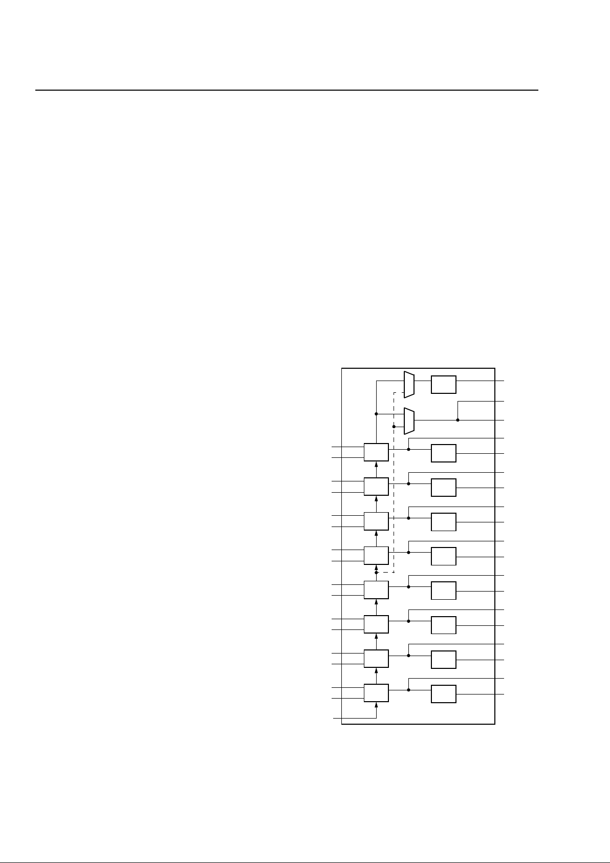
Figure 2. PFU Ports
The PFU can be configured to operate in four modes: logic mode, half-logic mode, ripple mode, and memory (RAM/
ROM) mode. In addition, ripple mode has four submodes and RAM mode can be used in either a single- or dualport memory fashion. These submodes of operation are discussed in the following sections.
F5D
K7_0
K7_1
K7_2
K7_3
K6_0
K6_1
K6_2
K6_3
K5_0
K5_1
K5_2
K5_3
K4_0
K4_1
K4_2
K4_3
F5C
DIN7
DIN6
DIN5
DIN4
DIN3
DIN2
DIN1
DIN0
CIN
F5B
K3_0
K3_1
K3_2
K3_3
K2_0
K2_1
K2_2
K2_3
K1_0
K1_1
K1_2
K1_3
K0_0
K0_1
K0_2
K0_3
F5A
PROGRAMMABLE
FUNCTION UNIT
(PFU)
Q7
Q6
Q5
Q4
Q3
Q2
Q1
Q0
COUT
REGCOUT
F7
F6
F5
F4
F3
F2
F1
F0
SEL[0:1]CE[0:1]CLK[0:1]LSR[0:1]
LUT603
LUT647
10 Lucent Technologies Inc.
Preliminary Data Sheet
December 2000
ORCA Series 4 FPGAs
Programmable Logic Cells
(continued)
5-9714(F)
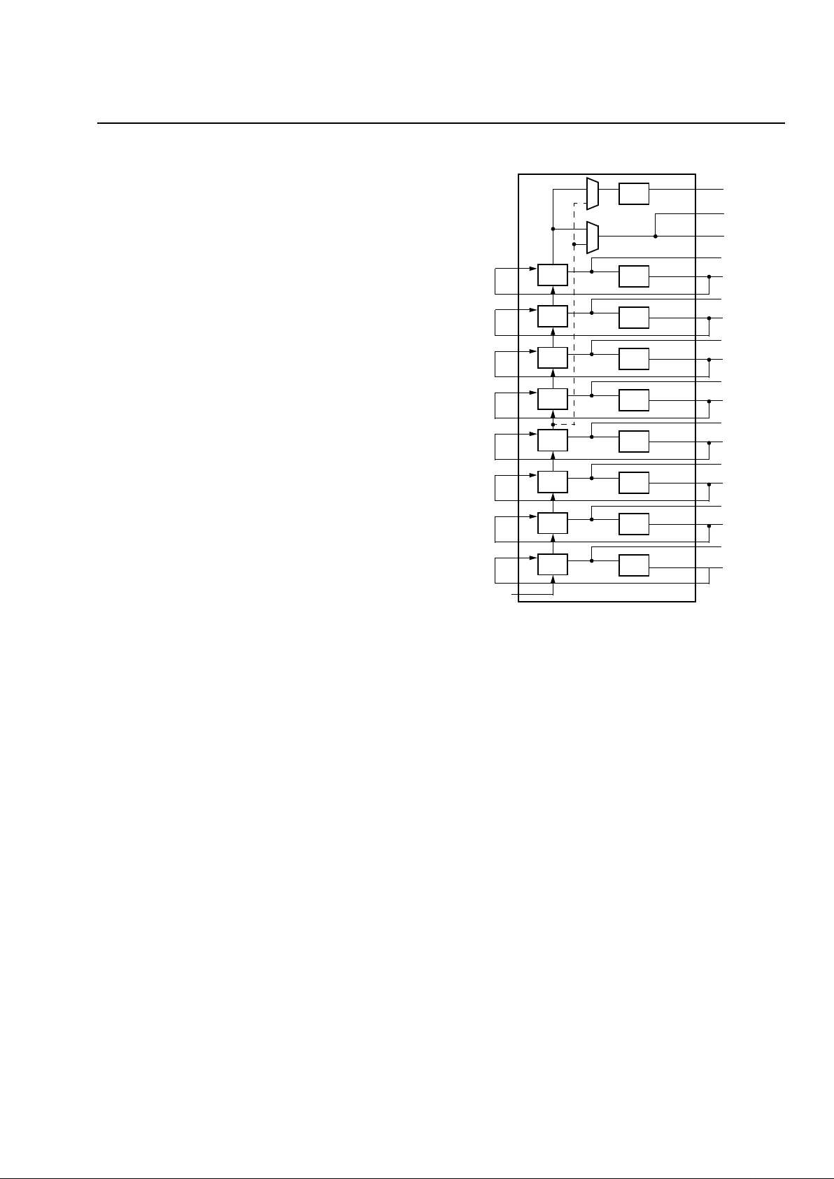
Note: All multiplexers without select inputs are configuration selector multiplexers.
Figure 3. Simplified PFU Diagram
K3_0MUX
K7_0MUX
D0
D1
SD
SP
CK
LSR
REG7
RESET
SET
Q7
F7
0
DIN7
DIN7MUX
D0
D1
SD
SP
CK
LSR
REG6
RESET
SET
Q6
F6
0
DIN6
DIN6MUX
D0
D1
SD
SP
CK
LSR
REG5
RESET
SET
Q5
F5
0
DIN5
DIN5MUX
D0
D1
SD
SP
CK
LSR
REG4
RESET
SET
Q4
F4
0
DIN4
DIN4MUX
LUT647
0
A
B
C
D
A
B
C
D
A
B
C
D
A
B
C
D
FSDMUX
K7_2MUX
K6_0MUX
K6_2MUX
AMUX
H7H6MUX
K7
K6
K5
K4
FSCMUX
H5H4MUX
LUT6MUX
F5D
K7_0
K7_1
K7_2
K7_3
K6_0
K6_1
K6_2
K6_3
K5_0
K5_1
K5_2
K5_3
K4_0
K4_1
K4_2
F5C
K4_3
D0
D1
SD
SP
CK
LSR
REG3
RESET
SET
Q3
F3
0
DIN3
DIN3MUX
D0
D1
SD
SP
CK
LSR
REG2
RESET
SET
Q2
F2
0
DIN2
DIN2MUX
D0
D1
SD
SP
CK
LSR
REG1
RESET
SET
Q1
F1
0
DIN1
DIN1MUX
D0
D1
SD
SP
CK
LSR
REG0
RESET
SET
DEL0
DEL1
DEL2
Q0
F0
0
DIN0
DIN0MUX
LUT603
0
A
B
C
D
A
B
C
D
A
B
C
D
A
B
C
D
FSBMUX
K3_2MUX
K2_0MUX
K2_2MUX
BMUX
H3H2MUX
K3
K2
K1
K0
F5AMUX
H1H0MUX
LUT6MUX
F5B
K3_0
K3_1
K3_2
K3_3
K2_0
K2_1
K2_2
K2_3
K1_0
K1_1
K1_2
K1_3
K0_0
K0_1
K0_2
F5A
K0_3
0
CLK1
CLK1MUX
0
SEL1
SEL1MUX
1
CE1
CE1MUX
CE47MUX
0
LSR1
LSR1MUX
LSR47MUX
0
CIN
1
0
0
CLK0
CLK0MUX
0
SEL0
SEL0MUX
1
CE0
CE0MUX
CEBMUX
0
LSR0
LSR0MUX
CE03MUX
1
0
LSRBMUX
LSR03MUX
1
0
D0
SP
CK
LSR
REG8
RESET
SET
RECCOUT
COUT
SR1MODEATTR
SR1MODE
CE1_OVER_LSR1
LSR1_OVER_CE1
RSYNC1
SR0MODEATTR
SR0MODE
CE0_OVER_LSR0
LSR0_OVER_CE0
ASYNC0
REGMODE_TOP
FF
LATCH
REG 4 THROUGH 7
THIS IS ALWAYS A FLIPFLOP
REGMODE_BOT
FF
LATCH
REG 0 THROUGH 3
LOGIC
MLOGIC
RIPPLE
RAM
ROM
ENABLED
DISABLED
GSR
PFU MODES
CINMUX
0
0
DEL3
DEL0
DEL1
DEL2
DEL3
DEL0
DEL1
DEL2
DEL3
DEL0
DEL1
DEL2
DEL3
DEL0
DEL1
DEL2
DEL3
DEL0
DEL1
DEL2
DEL3
DEL0
DEL1
DEL2
DEL3
DEL0
DEL1
DEL2
DEL3
DEL0
DEL1
DEL2
DEL3

Lucent Technologies Inc. 11
Preliminary Data Sheet
December 2000
ORCA Series 4 FPGAs
Programmable Logic Cells
(continued)
Look-Up Table Operatin g Modes
The operating mode affects the functionality of the PFU input and output ports and internal PFU routing. For example, in some operating modes, the DIN[7:0] inputs are direct data inputs to the PFU latches/FFs. In memory mode,
the same DIN[7:0] inputs are used as a 4-bit write data input bus and a 4-bit write address input bus
into LUT memory.
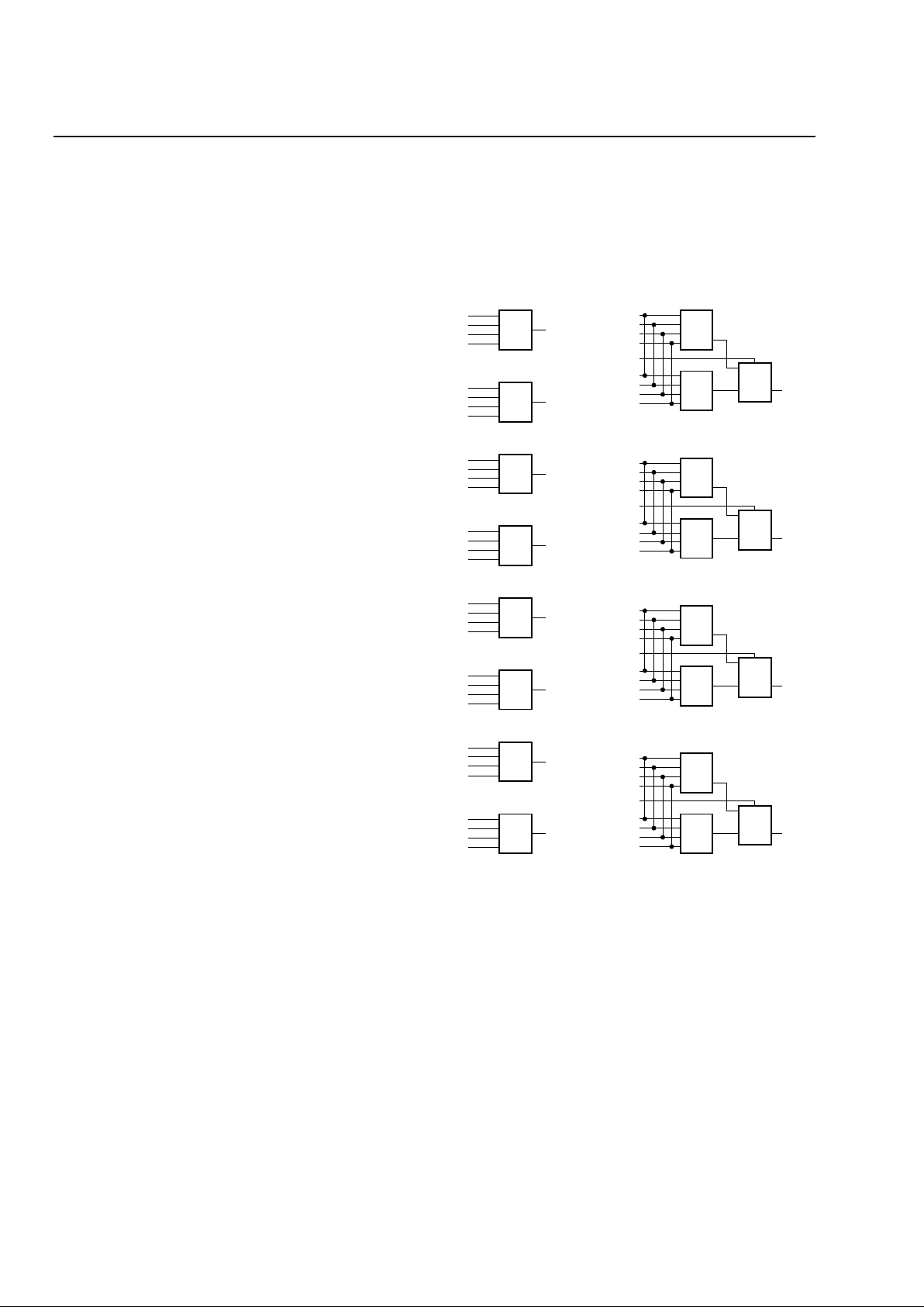
Table 3 lists the basic operating modes of the LUT. Figure 4—Figure 7 show block diagrams of the LUT operating
modes. The accompanying descriptions demonstrate each mode’s use for generating logic.
Table 3. Look-Up Table Operating Modes
PFU Control Inputs
Each PFU has eight routable control inputs and an active-low, asynchronous global set/reset (GSRN) signal that
affects all latches and FFs in the device. The eight control inputs are CLK[1:0], LSR[1:0], CE[1:0], and SEL[1:0],
and their functionality for each logic mode of the PFU is shown in Table 4. The clock signal to the PFU is CLK, CE
stands for clock enable, which is its primary function. LSR is the local set/reset signal that can be configured as synchronous or asynchronous. The selection of set or reset is made for each latch/FF and is not a function of the signal
itself. SEL is used to dynamically select between direct PFU input and LUT output data as the input to
the latches/FFs.
All of the control signals can be disabled and/or inverted via the configuration logic. A disabled clock enable
indicates that the clock is always enabled. A disabled LSR indicates that the latch/FF never sets/resets (except from
GSRN). A disabled SEL input indicates that DIN[7:0] PFU inputs or the LUT outputs are always input to the latches/
FFs.
Table 4. Control Input Functionality
Mode Function
Logic 4-, 5-, and 6-input LUTs; softwired LUTs; latches/FFs with direct input or LUT input; CIN as direct
input to ninth FF or as pass through to COUT.
Half Logic/
Half Ripple
Upper four LUTs and latches/FFs in logic mode; lower four LUTs and latches/FFs in ripple mode;
CIN and ninth FF for logic or ripple functions.
Ripple All LUTs combined to perform ripple-through data functions. Eight LUT registers available for
direct-in use or to register ripple output. Ninth FF dedicated to ripple out, if used. The submodes of
ripple mode are adder/subtractor, counter, multiplier, and comparator.
Memory All LUTs and latches/FFs used to create a 32x4 synchronous dual-port RAM. Can be used as
single-port or as ROM.
Mode CLK[1:0] LSR[1:0] CE[1:0] SEL[1:0]
Logic CLK to all latches/
FFs
LSR to all latches/FFs,
enabled per nibble and
for ninth FF
CE to all latches/FFs,
selectable per nibble
and for ninth FF
Select between LUT
input and direct input for
eight latches/FFs
Half Logic/
Half Ripple
CLK to all latches/
FFs
LSR to all latches/FF,
enabled per nibble and
for ninth FF
CE to all latches/FFs,
selectable per nibble
and for ninth FF
Select between LUT
input and direct input for
eight latches/FFs
Ripple CLK to all latches/
FFs
LSR to all latches/FFs,
enabled per nibble and
for ninth FF
CE to all latches/FFs,
selectable per nibble
and for ninth FF
Select between LUT
input and direct input for
eight latches/FFs
Memory
(RAM)
CLK to RAM LSR0 port enable 2 CE1 RAM write enable
CE0 Port enable 1
Not used
Memory
(ROM)
Optional for
synchronous outputs
Not used Not used Not used
12 Lucent Technologies Inc.
Preliminary Data Sheet
December 2000
ORCA Series 4 FPGAs
Programmable Logic Cells
(continued)
Logic Mode
The PFU diagram of Figure 3 represents the logic
mode of operation. In logic mode, the eight LUTs are
used individually or in flexible groups to implement user
logic functions. The latches/FFs may be used in conjunction with the LUTs or separately with the direct
PFU data inputs. There are three basic submodes of
LUT operation in PFU logic mode: F4 mode, F5 mode,
and the F6 mode. Combinations of the submodes are
possible in each PFU.
F4 mode, shown simplified in Figure 4, illustrates the
uses of the basic 4-input LUTs in the PFU. The output
of an F4 LUT can be passed out of the PFU, captured
at the LUTs associated latch/FF, or multiplexed with the
adjacent F4 LUT output using one of the F5[A:D] inputs
to the PFU (not shown). Only adjacent LUT pairs (K
0
and K
1
, K2 and K3, K4 and K5, K6 and K7) can be multiplexed, and the output always goes to the even-numbered output of the pair.
The F5 submode of the LUT operation, shown simplified in Figure 4, indicates the use of 5-input LUTs to
implement logic. 5-input LUTs are created from two
4-input LUTs and a multiplexer. The F5 LUT is the
same as the multiplexing of two F4 LUTs described
previously with the constraint that the inputs to both F4
LUTs be the same. The F5[A:D] input is then used as
the fifth LUT input. The equations for the two F4 LUTs
will differ by the assumed value for the F5[A:D] input,
one F4 LUT assuming that the F5[A:D] input is zero,
and the other assuming it is a one. The selection of the
appropriate F4 LUT output in the F5 MUX by the
F5[A:D] signal creates a 5-input LUT.
Two 6-input LUTs are created by shorting together the
inputs of four 4-input LUTs (K0:3 and K4:7) which are
multiplexed together. The F5 inputs of the adjacent F4
LUTs derive the fifth and sixth inputs of the F6 mode as
shown in Figure 5. The F6 outputs, LUT603 and
LUT647, are dedicated to the F6 mode or can be used
as the outputs of MUX8x1. MUX8x1 modes as shown
in Figure 7 are created by programming adjacent
4-input LUTs to 2x1 MUXs and multiplexing down to
create MUX8x1. Other functions can be implemented
from the configuration shown in Figure 5 where the four
LUT4s drive the 4x1 MUX in each half of the PFU if the
LUT4 inputs are not tied to the same inputs. Both F6
mode and MUX8x1 are available in the upper and
lower PFU nibbles.
Any combination of F4 and F5 LUTs is allowed per
PFU using the eight 16-bit LUTs. Examples are eight
F4 LUTs, four F5 LUTs, a combination of four F4 plus
two F5 LUTs, a combination of two F4, one F5, plus
one F6, or a combination of one F5, one MUX21 of two
LUT4s, and one MUX41 of four LUT4s.
5-9733(F)
Figure 4. Simplified F4 and F5 Logic Modes
K7_0
K7_1
K7_2
F5D
LUT4
LUT4
2x1
MUX
F6
K7_3
K6_0
K6_1
K6_2
K6_3
K5_0
K5_1
K5_2
F5C
LUT4
LUT4
2x1
MUX
F4
K5_3
K4_0
K4_1
K4_2
K4_3
K3_0
K3_1
K3_2
F5B
LUT4
LUT4
2x1
MUX
F2
K3_3
K2_0
K2_1
K2_2
K2_3
K1_0
K1_1
K1_2
F5A
LUT4
LUT4
2x1
MUX
F0
K1_3
K0_0
K0_1
K0_2
K0_3
K7 F7
K6 F6
K5 F5
K4 F4
K3 F3
K2 F2
K1 F1
K0 F0
Lucent Technologies Inc. 13
Preliminary Data Sheet
December 2000
ORCA Series 4 FPGAs
Programmable Logic Cells
(continued)
5-9734(F)a
Figure 5. Simplified F6 Logic Modes
5-9735(F)
Figure 6. MUX 4x1
K7_0
K7_1
K7_2
K7_3
K6_0
K6_1
K6_2
K6_3
K5_0
K5_1
K5_2
K5_3
K4_0
K4_1
K4_2
K4_3
F5D
F5C
LUT4
LUT4
LUT4
LUT4
4x1
MUX
K3_0
K3_1
K3_2
K3_3
K2_0
K2_1
K2_2
K2_3
K1_0
K1_1
K1_2
K1_3
K0_0
K0_1
K0_2
K0_3
F5B
F5A
LUT4
LUT4
LUT4
LUT4
LUT603
4x1
MUX
LUT647
K7_0
K7_1
K7_2
F5D
LUT4
LUT4
2x1
MUX
K6_0
K6_1
K6_2
F4
K5_0
K5_1
K5_2
F5C
LUT4
LUT4
2x1
MUX
K4_0
K4_1
K4_2
F3
K3_0
K3_1
K3_2
F5B
LUT4
LUT4
2x1
MUX
K2_0
K2_1
K2_2
F2
K1_0
K1_1
K1_2
F5A
LUT4
LUT4
2x1
MUX
K0_0
K0_1
K0_2
F0
14 Lucent Technologies Inc.
Preliminary Data Sheet
December 2000
ORCA Series 4 FPGAs
Programmable Logic Cells
(continued)
5-9736(F)a
Figure 7. MUX 8x1
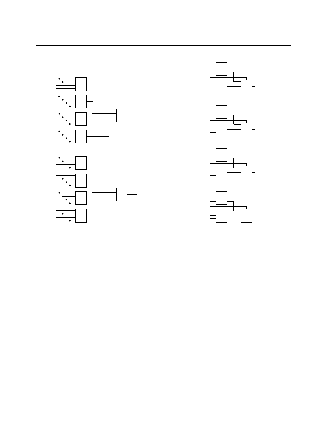
Softwired LUT capability uses F4, F5, and F6 LUTs, along with MUX21 and MUX41 blocks together with internal
PFU feedback routing, to generate complex logic functions up to three LUT levels deep. Multiplexers can be independently configured to route certain LUT outputs to the input of other LUTs. In this manner, very complex logic
functions, some of up to 22 inputs, can be implemented in a single PFU at greatly enhanced speeds.
It is important to note that an LUT output that is fed back for softwired use is still available to be registered or output
from the PFU. This means, for instance, that a logic equation that is needed by itself and as a term in a larger equation need only be generated once, and PLC routing resources will not be required to use it in the larger equation.
K7_0
K7_1
K7_2
F5D
LUT4
LUT4
K6_0
K6_1
K6_2
LUT4
LUT4
K5_0
K5_1
K5_2
K4_0
K4_1
K4_2
F5C
LUT4
K3_0
K3_1
K3_2
F5B
LUT4
LUT4
K2_0
K2_1
K2_2
LUT4
LUT4
K1_0
K1_1
K1_2
K0_0
K0_1
K0_2
F5A
LUT4
MUX8x1
4x1
MUX
4x1
MUX
[LUT647]
MUX8x1
[LUT603]
Lucent Technologies Inc. 15
Preliminary Data Sheet
December 2000
ORCA Series 4 FPGAs
Programmable Logic Cells
(continued)
5-5753 (F)
5-5754 (F)
Figure 8. Softwired LUT Topology Examples
F4
F4
F4
F4
F4
F4
F4
F4
FOUR 7-INPUT FUNCTIONS IN ONE PFU
F5
F5
F5
F5
TWO 9-INPUT FUNCTIONS IN ONE PFU
F5
F5
F5
F5
ONE 17-INPUT FUNCTION IN ONE PFU
F5
F5
F4
ONE 21-INPUT FUNCTION IN ONE PFU
F4 F4 F4
F4
F4
F4
F4
TWO 10-INPUT FUNCTIONS IN ONE PFU
F4
F4
F4
F4
3
ONE OF TWO 21-INPUT FUNCTIONS IN ONE PFU
ONE 22-INPUT FUNCTION IN ONE PFU
F5
F6
F4F4 F4 F4
F4 F54-INPUT LUT 5-INPUT LUT F6
6-INPUT LUT
16 Lucent Technologies Inc.
Preliminary Data Sheet
December 2000
ORCA Series 4 FPGAs
Programmable Logic Cells
(continued)
Half-Logic Mode
Series 4 FPGAs are based upon a twin-quad architecture in the PFUs. The bytewide nature (eight LUTs,
eight latches/FFs) may just as easily be viewed as two
nibbles (two sets of four LUTs, four latches/FFs). The
two nibbles of the PFU are organized so that any nibblewide feature (excluding some softwired LUT topologies) can be swapped with any other nibblewide f eature
in another PFU. This provides for very flexible use of
logic and for extremely flexible routing. The half-logic
mode of the PFU takes advantage of the twin-quad
architecture and allows half of a PFU, K
[7:4]
and associated latches/FFs, to be used in logic mode while the
other half of the PFU, K
[3:0]
and associated
latches/FFs, is used in ripple mode. In half-logic mode,
the ninth FF may be used as a general-purpose FF or
as a register in the ripple mode carry chain.
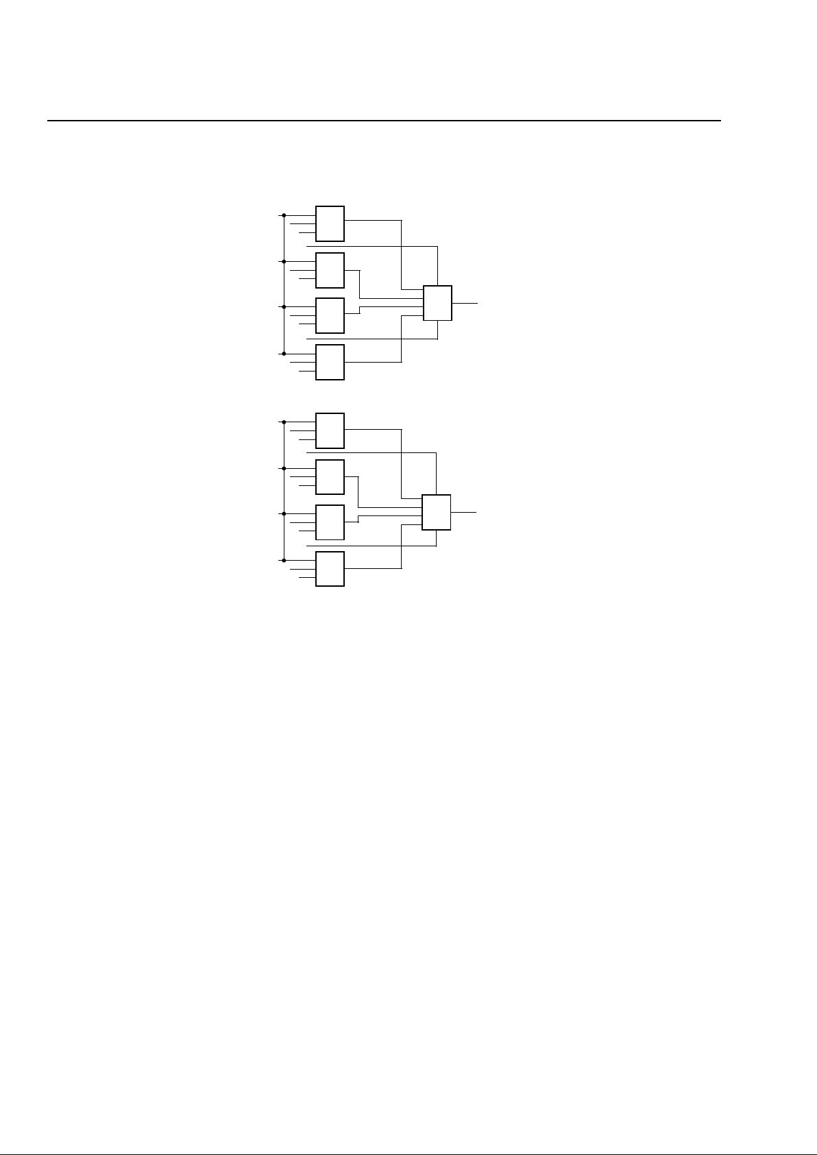
Ripple Mode
The PFU LUTs can be combined to do bytewide ripple
functions with high-speed carry logic. Each LUT has a
dedicated carry-out net to route the carry to/from any
adjacent LUT. Using the internal carry circuits, fast
arithmetic, counter, and comparison functions can be
implemented in one PFU. Similarly, each PFU has
carry-in (CIN, FCIN) and carry-out (COUT, FCOUT)
ports for fast-carry routing between adjacent PFUs.
The ripple mode is generally used in operations on two
data buses. A single PFU can support an 8-bit ripple
function. Data buses of 4 bits and less can use the
nibblewide ripple chain that is available in half-logic
mode. This nibblewide ripple chain is also useful for
longer ripple chains where the length modulo 8 is four
or less. For example, a 12-bit adder (12 modulo 8 = 4)
can be implemented in one PFU in ripple mode (8 bits)
and one PFU in half-logic mode (4 bits), freeing half of
a PFU for general logic mode functions.
Each LUT has two operands and a ripple (generally
carry) input, and provides a result and ripple (generally
carry) output. A single bit is rippled from the previous
LUT and is used as input into the current LUT. For LUT
K
0
, the ripple input is from the PFU CIN or FCIN port.
The CIN/FCIN data can come from either the fast-carry
routing (FCIN) or the PFU input (CIN), or it can be tied
to logic 1 or logic 0.
In the following discussions, the notations LUT K
7/K3
and F[7:0]/F[3:0]
are used to denote the LUT that provides the carry-out and the data outputs for full PFU
ripple operation (K
7
, F[7:0]) and half-logic ripple
operation (K
3
, F[3:0]), respectively. The ripple mode
diagram (Figure 9) shows full PFU ripple operation,
with half-logic ripple connections shown as dashed
lines.
The result output and ripple output are calculated by
using generate/propagate circuitry. In ripple mode, the
two operands are input into K
Z
[1] and KZ[0] of each
LUT. The result bits, one per LUT , are F[7:0]/F[3:0]
(see
Figure 9). The ripple output from LUT K
7/K3
can be
routed on dedicated carry circuitry into any of four adjacent PLCs, and it can be placed on the PFU COUT/
FCOUT outputs. This allows the PLCs to be cascaded
in the ripple mode so that nibblewide ripple functions
can be expanded easily to any length.
Result outputs and the carry-out may optionally be registered within the PFU. The capability to register the
ripple results, including the carry output, provides for
improved counter performance and simplified pipelining in arithmetic functions.
5-5755(F).
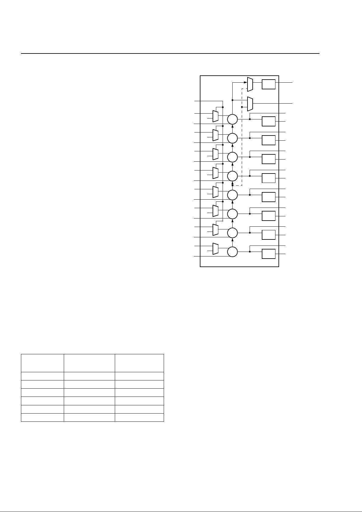
Figure 9. Ripple Mode
F7
K
7
[1]
K
7
[0]
K7
DQ
C
C
DQ
Q7
REGOUT
COUT
F6
K
6
[1]
K
6
[0]
K6
DQ
Q6
F4
K
4
[1]
K
4
[0]
K4
DQ
Q4
F3
K
3
[1]
K
3
[0]
K3
DQ
Q3
F2
K
2
[1]
K
2
[0]
K2
DQ
Q2
F1
K
1
[1]
K
1
[0]
K1
DQ
Q1
F5
K
5
[1]
K
5
[0]
K5
DQ
Q5
F0
K
0
[1]
K
0
[0]
K0
DQ
Q0
IN/FCIN
FCOUT
Lucent Technologies Inc. 17
Preliminary Data Sheet
December 2000
ORCA Series 4 FPGAs
Programmable Logic Cells
(continued)
The ripple mode can be used in one of four submodes.
The first of these is
adder-subtractor submode
. In
this submode, each LUT generates three separate outputs. One of the three outputs selects whether the
carry-in is to be propagated to the carry-out of the current LUT or if the carry-out needs to be generated. If
the carry-out needs to be generated, this is provided by
the second LUT output. The result of this selection is
placed on the carry-out signal, which is connected to
the next LUT carry-in or the COUT/FCOUT signal, if it
is the last LUT (K
7/K3
). Both of these outputs can be
any equation created from K
Z
[1] and KZ[0], but in this
case, they have been set to the propagate and generate functions.
The third LUT output cre ates th e result b it f or each LU T
output connected to F[7:0]/F[3:0]. If an adder/subtractor is needed, the control signal to select addition or
subtraction is input on F5A/F5C inputs. These inputs
generate the controller input AS. When AS = 0, this
function performs the adder, A + B. When AS = 1, the
function performs the subtractor, A – B. The result bit is
created in one-half of the LUT from a single bit from
each input bus K
Z
[1:0], along with the ripple input bit.
The second submode is the
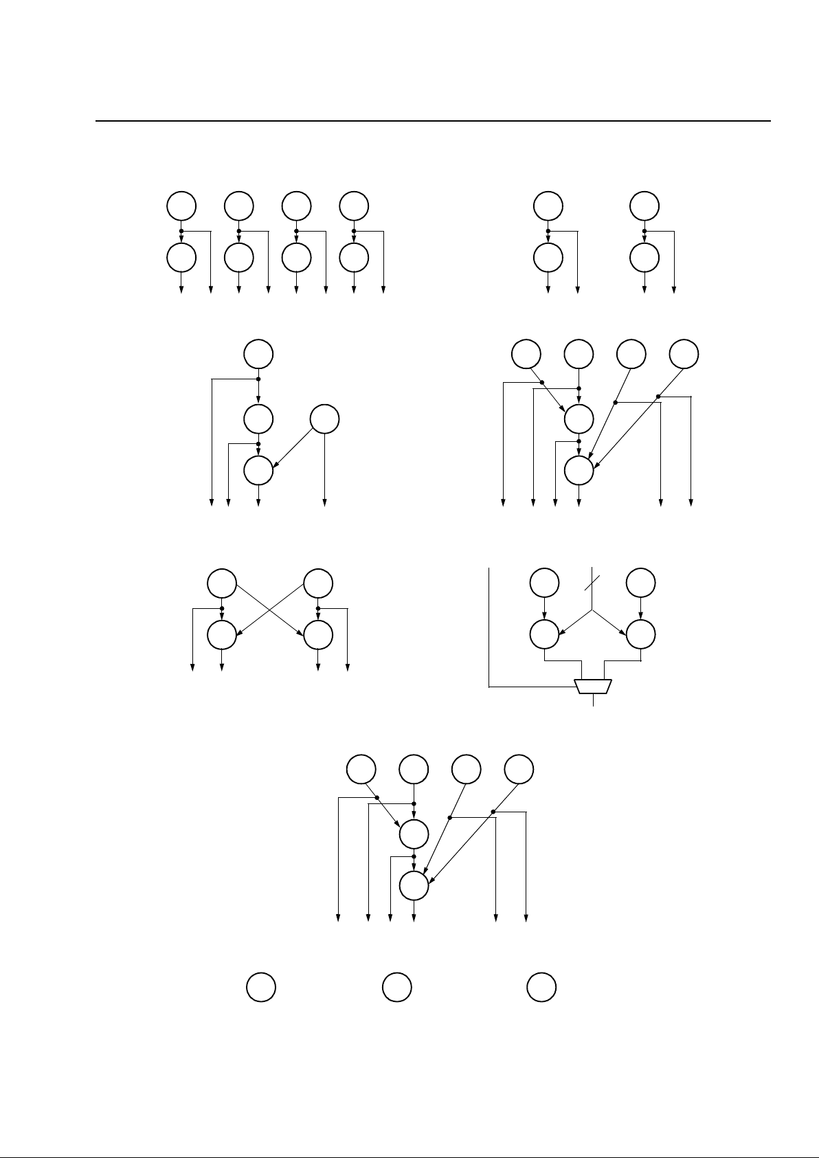
counter submode
(see
Figure 10) . T he present count, wh ic h m ay be initia l ized
via the PFU DIN inputs to the latches/FFs, is supplied
to input K
Z
[0], and then output F[7:0]/F[3:0] will either
be incremented by one for an up counter or decremented by one for a down counter. If an up/down
counter is needed, the control signal to select the direction (up or down) is input on F5A and F5C. When
F5[A:C], respectively per nibble, is a logic 1, this indicates a down counter and a logic 0 indicates an up
counter.
5-5756(F)
Figure 10. Counter Submode
F7
K
7
[0]
K7
DQ
C
C
DQ
Q7
REGCOUT
COUT
F6
K
6
[0]
K6
DQ
Q6
F4
K
4
[0]
K4
DQ
Q4
F3
K
3
[0]
K3
DQ
Q3
F2
K
2
[0]
K2
DQ
Q2
F1
K
1
[0]
K1
DQ
Q1
F5
K
5
[0]
K5
DQ
Q5
F0
K
0
[0]
K0
DQ
Q0
CIN/FCIN
FCOUT
18 Lucent Technologies Inc.
Preliminary Data Sheet
December 2000
ORCA Series 4 FPGAs
Programmable Logic Cells
(continued)
In the third submode,
multiplier submode
, a single
PFU can affect an 8x1 bit (4x1 for half-ripple mode)
multiply and sum with a partial product (see Figure 11).
The multiplier bit is input at F5[A:C], respectively per
nibble, and the multiplicand bits are input at K
Z
[1],
where K
7
[1] is the most significant bit (MSB). KZ[0] contains the partial product (or other input to be summed)
from a previous stage. If F5[A:C] is logical 1, the multiplicand is added to the partial product. If F5[A:C] is logical 0, 0 is added to the partial product, which is the
same as passing the partial product. CIN/FCIN can
bring the carry-in from the less significant PFUs if the
multiplicand is wider than 8 bits, and COUT/FCOUT
holds any carry-out from the multiplication, which may
then be used as part of the product or routed to another
PFU in multiplier mode for multiplicand width expansion.
Ripple mode’s fourth submode features
equality
comparators
. The functions that are explicitly available
are A
≥
B, A
≠
B, and A ≤ B, where the value for A is
input on K
Z
[0], and the value for B is input on KZ[1]. A
value of 1 on the carry-out signals valid argument. For
example, a carry-out equal to 1 in AB submode indicates that the value on K
Z
[0] is greater than or equal to
the value on K
Z
[1]. Conversely, the functions A ≤ B,
A + B, and A > B are available using the same functions
but with a 0 output expected. For example, A
>
B with a
0 output i ndicates A
≤
B. Table 5 shows each function
and the output expected.
If larger than 8 bits, the carry-out signal can be cas-
caded using fast-carry logic to the carry-in of any adjacent PFU. The use of this submode could be shown
using Figure 9, except that the CIN/FCIN input for the
least significant PFU is controlled via configuration.
Table 5. Ripple Mode Equality Comparator
Functions and Outputs
5-5757(F)
Key: C = configuration data.
Note: F5[A:C] shorted together.
Figure 11. Multiplier Submode
Equality
Function
ORCA Foundry
Submode
True, if
Carry-Out Is:
A
≥
BA ≥ B1
A
≤
BA ≤ B1
A
≠
BA
≠
B1
A < B A > B 0
A > B A < B 0
A = B A ≠ B0
K7[1]
K7[0]
+
D
Q
C
C
DQ
1
00
K7
F5[A:C]
K4[1]
K4[0]
+
D
Q
1
00
K4
K3[1]
K3[0]
+
D
Q
1
00
K3
K2[1]
K2[0]
+
D
Q
1
00
K2
K1[1]
K1[0]
+
D
Q
1
00
K1
K6[1]
K6[0]
+
D
Q
1
00
K6
K5[1]
K5[0]
+
D
Q
1
00
K5
K0[1]
K0[0]
+
D
Q
1
00
K0
Q0
F0
Q1
F1
Q2
F2
Q3
F3
Q4
F4
Q5
F5
Q6
F6
Q7
F7
COUT
REGCOUT
Lucent Technologies Inc. 19
Preliminary Data Sheet
December 2000
ORCA Series 4 FPGAs
Programmable Logic Cells
(continued)
Memory Mode
The Series 4 PFU can be used to implement a 32 x 4 (128-bit) synchronous, dual-port RAM. A block diagram of a
PFU in memory mode is shown in Figure 12. This RAM can also be configured to work as a single-port memory
and because initial values can be loaded into the RAM during configuration, it can also be used as a ROM.
5-5969(F)a
1. CLK[0:1] are commonly connected in memory mode.
2. CE1 = write enable = wren; wren = 0 (no write enable); wren = 1 (write enabled).
CE0 = write port enable 0; CE0 = 0, wren = 0; CE0 = 1, wren = CE1.
LSR0 = write port enable 1; LSR0 = 0, wren = CE0; LSR0 = 1, wren = CE1.
Figure 12. Memory Mode
Q6
Q4
Q2
Q0
D5Q
CIN(WA1)
KZ[3:0]
4
F5[A:D]
D Q
DIN7(WA3)
D Q
DIN5(WA2)
D Q
DIN3(WA1)
D Q
DIN1(WA0)
D Q
DIN6(WD3)
D Q
DIN4(WD2)
D Q
DIN2(WD1)
D Q
DIN0(WD0)
D Q
CE0, LSR0
S/E
CLK[0:1]
4
WRITE
WRITE
READ
READ
4
F6
F4
F2
F0
D Q
D Q
D Q
D Q
WRITE
RAM CLOCK
ADDRESS[4:0]
ADDRESS[4:0]
DATA[3:0]
DATA[3:0]
ENABLE
(SEE NOTE 2.)
CE1

20 Lucent Technologies Inc.
Preliminary Data Sheet
December 2000
ORCA Series 4 FPGAs
Programmable Logic Cells
(continued)
The PFU memory mode uses all LUTs and latches/FFs
including the ninth FF in its implementation as shown in
Figure 12. The read address is input at the K
Z
[3:0] and
F5[A:D] inputs where K
Z
[0] is the LSB and F5[A:D] is
the MSB, and the write address is input on CIN (MSB)
and DIN[7, 5, 3, 1], with DIN[1] being the LSB. Write
data is input on DIN[6, 4, 2, 0], where DIN[6] is the
MSB, and read data is available combinatorially on
F[6, 4, 2, 0] and registered on Q[6, 4, 2, 0] with F[6] and
Q[6] being the MSB. The write enable controlling ports
are input on CE0, CE1, and LSR0. CE1 is the activehigh write enable (CE1 = 1, RAM is write enabled). The
first write port is enabled by CE0. The second write
port is enabled with LSR0. The PFU CLK (CLK0) signal
is used to synchronously write the data. The polarities
of the clock, write enable, and port enables are all programmable. Write-port enables may be disabled if they
are not to be used.
Data is written to the write data, write address, and
write enable registers on the active edge of the clock,
but data is not written into the RAM until the next clock
edge one-half cycle later. The read port is actually
asynchronous, providing the user with read data very
quickly after setting the read address, but timing is also
provided so that the read port may be treated as fully
synchronous for write then read applications. If the
read and write address lines are tied together (maintaining MSB to MSB, etc.), then the dual-port RAM
operates as a synchronous single-port RAM. If the
write enable is disabled, and an initial memory contents
are provided at configuration time, the memory acts as
a ROM (the write data and write address ports and
write port enables are not used).
Wider memories can be created by operating two or
more memory mode PFUs in parallel, all with the same
address and control signals, but each with a different
nibble of data. To increase memory word depth above
32, two or more PLCs can be used. Figure 10 shows a
128 x 8 dual-port RAM that is implemented in eight
PLCs. This figure demonstrates data path width expansion by placing two memories in parallel to achieve an
8-bit data path. Depth expansion is applied to achieve
128 words deep using the 32-word deep PFU memories. In addition to the PFU in each PLC, the SLIC
(described in the next section) in each PLC is used for
read address decodes and 3-state drivers. The 128 x 8
RAM shown could be made to operate as a single-port
RAM by tying (bit-for-bit) the read and write addresses.
To achieve depth expansion, one or two of the write
address bits (generally the MSBs) are routed to the
write port enables as in Figure 10. For 2 bits, the bits
select which 32-word bank of RAM of the four available
from a decode of two WPE inputs is to be written. Similarly, 2 bits of the read address are decoded in the
SLIC and are used to control the 3-state buffers
through which the read data passes. The write data
bus is common, with separate nibbles for width expansion, across all PLCs, and the read data bus is common (again, with separate nibbles) to all PLCs at the
output of the 3-state buffers.
Figure 13 also shows the capability to provide a read
enable for RAMs/ROMs using the SLIC cell. The read
enable will 3-state the read data bus when inactive,
allowing the write data and read data buses to be tied
together if desired.

Preliminary Data Sheet
December 2000
Lucent Technologies Inc. 21
ORCA Series 4 FPGAs
Programmable Logic Cells
(continued)
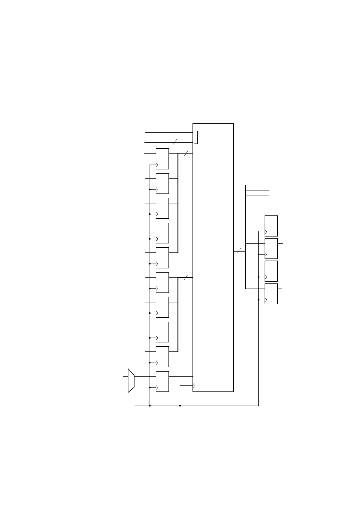
5-5749(F)
Figure 13. Memory Mode Expansion Example—128 x 8 RAM
RD[7:0]
WE
WA[6:0]
RA[6:0]
CLK
WA RA
WPE 1
WPE 2
WE
WD[7:4]
5 5
4
PLC
8
WD[7:0]
8
7
7
WA RA
WPE 1
WPE 2
WE
RD[3:0]
WD[3:0]
5 5
4
PLC
RD[7:4]
WA RA
WPE 1
WPE 2
WE
WD[7:4]
5 5
4
PLC
WA RA
WPE 1
WPE 2
WE
RD[3:0]
WD[3:0]
5 5
4
PLC
RD[7:4]
RE
RE
4
RE
4
RE
4
RE
4
Supplemental Logic and Interconnect Cell
Each PLC contains a SLIC embedded within the PLC
routing, outside of the PFU. As its name indicates, the
SLIC performs both logic and interconnect (routing)
functions. Its main features are 3-statable, bidirectional
buffers, and a PAL-like decoder capability. Figure 14
shows a diagram of a SLIC with all of its features
shown. All modes of the SLIC are not available at one
time.
The ten SLIC inputs can be sourced directly from the
PFU or from the general routing fabric. SI[0:9] inputs
can come from the horizontal or vertical routing, and
I[0:9} comes from the PFU outputs O[9:0]. These
inputs can also be tied to a logical 1 or 0 constant. The
inputs are twin-quad in nature and are segregated into
two groups of four nibbles and a third group of two
inputs for control. Each input nibble groups also have
3-state capability; however, the third pair does not.
There is one 3-state control (TRI) for each SLIC, with
the capability to invert or disable the 3-state control for
each group of four BIDIs. Separate 3-state control for
each nibblewide group is achievable by using the
SLICs decoder (DEC) output, driven by the group of
two BIDIs, to control the 3-state of one BIDI nibble
while using the TRI signal to control the 3-state of the
other BIDI nibble. Figure 15
shows the SLIC in buffer
mode with available 3-state control from the TRI and
DEC signals. If the entire SLIC is acting in a buffer
capacity, the DEC output may be used to generate a
constant logic 1 (V
HI
) or logic 0 (VLO) signal for general
use.
The SLIC may also be used to generate PAL-like AND-
OR with optional INVERT (AOI) functions or a decoder
of up to 10 bits. Each group of buffers can feed into an
AND gate (4-input AND for the nibble groups and
2-input AND for the other two buffers). These AND
gates then feed into a 3-input gate that can be configured as either an AND gate or an OR gate. The output
of the 3-input gate is invertible and is output at the DEC
output of the SLIC. Figure 19 shows the SLIC in full
decoder mode.
The functionality of the SLIC is parsed by the two
nibblewide groups and the 2-bit buffer group. Each of
these groups may operate independently as BIDI buffers (with or without 3-state capability for the nibblewide
groups) or as a PAL/decoder.
22 Lucent Technologies Inc.
Preliminary Data Sheet
December 2000
ORCA Series 4 FPGAs
Programmable Logic Cells
(continued)
As discussed in the Memory Mode section on page 19,
if the SLIC is placed into one of the modes where it
contains both buffers and a decode or AOI function
(e.g., BUF_BUF_DEC mode), the DEC output can be
gated with the 3-state input signal. This allows up to a
6-input decode (e.g., BUF_DEC_DEC mode) plus the
3-state input to control the enable/disable of up to four
buffers per SLIC. Figure 15—Figure 19 show several
configurations of the SLIC, while Table 6 shows all of
the possible modes.
Table 6. SLIC Modes
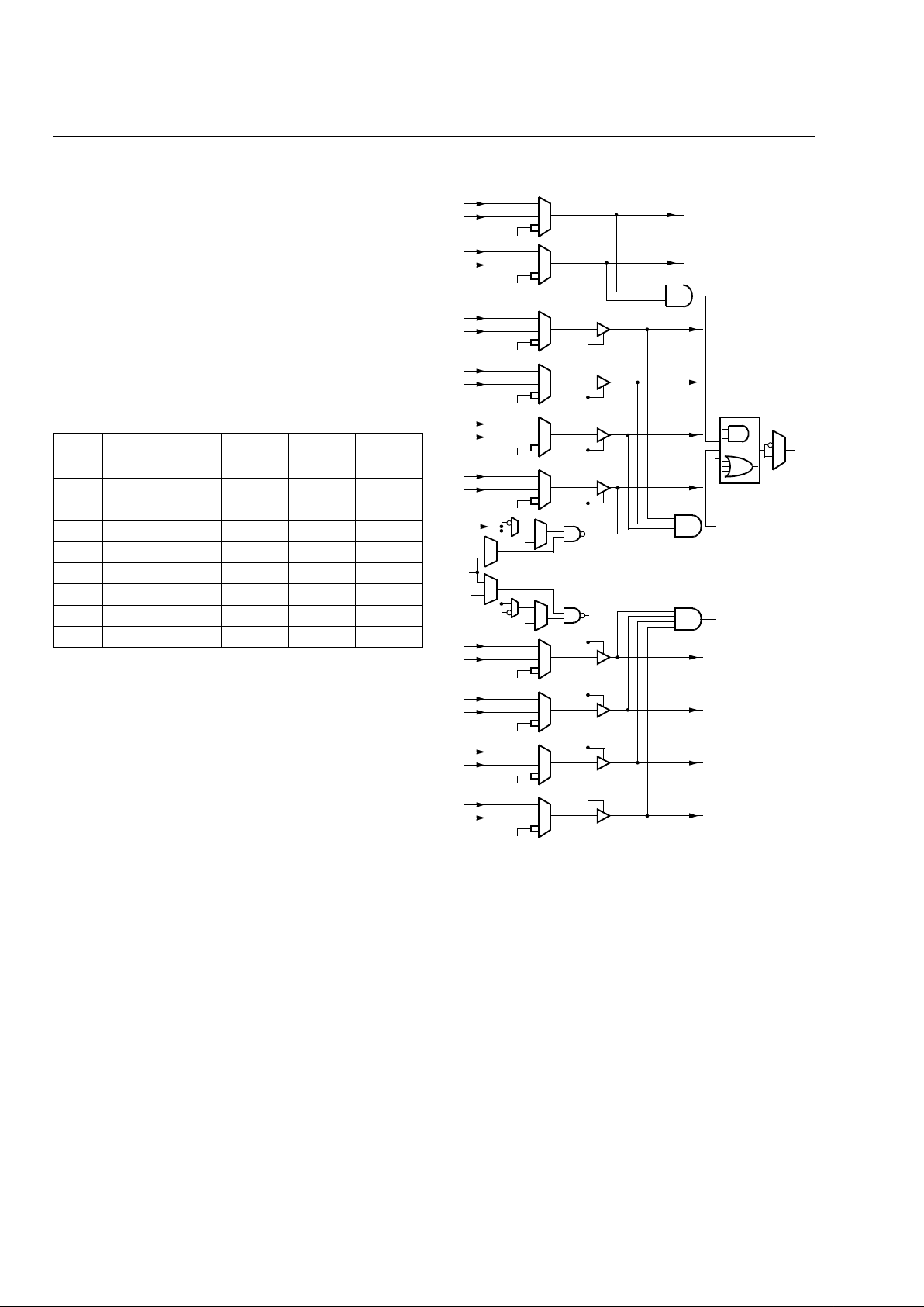
5-5744(F).a.
Figure 14. SLIC All Modes Diagram
Mode
No.
Mode BUF
[3:0]
BUF
[7:4]
BUF
[9:8]
1 BUFFER Buffer Buffer Buffer
2 BUF_BUF_DEC Buffer Buffer Decoder
3 BUF_DEC_BUF Buffer Decoder Buffer
4
BUF_DEC_DEC
Buffer Decoder Decoder
5 DEC_BUF_BUF Decoder Buffer Buffer
6
DEC_BUF_DEC
Decoder Buffer Decoder
7
DEC_DEC_BUF
Decoder Decoder Buffer
8 DECODER Decoder Decoder Decoder
SIN9
I9
SOUT09
DEC
DEC
0/1
0/1
TRI
0/1
0/1
SOUT08
SOUT07
SOUT06
SOUT05
SOUT04
SOUT03
SOUT02
SOUT01
SOUT00
LOGIC 1 OR 0
SIN8
I8
LOGIC 1 OR 0
SIN7
I7
LOGIC 1 OR 0
SIN6
I6
LOGIC 1 OR 0
SIN5
I5
LOGIC 1 OR 0
SIN4
I4
LOGIC 1 OR 0
SIN3
I3
LOGIC 1 OR 0
SIN2
I2
LOGIC 1 OR 0
SIN1
I1
LOGIC 1 OR 0
SIN0
I0
LOGIC 1 OR 0
Lucent Technologies Inc. 23
Preliminary Data Sheet
December 2000
ORCA Series 4 FPGAs
Programmable Logic Cells
(continued)
5-5745(F).a
Figure 15. Buffer Mode
5-5746(F).a
Figure 16. Buffer-Buffer-Decoder Mode
SOUT08
TRI
0/1
0/1
1
0
DEC
THIS CAN BE USED TO GENERATE
A V
HI
OR VLO.
SIN8
I8
LOGIC 1 OR 0
SOUT09
SIN9
I9
LOGIC 1 OR 0
SOUT07
SIN7
I7
LOGIC 1 OR 0
SOUT06
SIN6
I6
LOGIC 1 OR 0
SOUT05
SIN5
I5
LOGIC 1 OR 0
SOUT04
SIN4
I4
LOGIC 1 OR 0
SOUT03
SIN3
I3
LOGIC 1 OR 0
SOUT02
SIN2
I2
LOGIC 1 OR 0
SOUT01
SIN1
I1
LOGIC 1 OR 0
SOUT00
SIN0
I0
LOGIC 1 OR 0
TRI
DEC
1
1
1
1
SOUT07
SIN7
I7
LOGIC 1 OR 0
SOUT06
SIN6
I6
LOGIC 1 OR 0
SOUT05
SIN5
I5
LOGIC 1 OR 0
SOUT04
SIN4
I4
LOGIC 1 OR 0
SIN9
I9
LOGIC 1 OR 0
SIN8
I8
LOGIC 1 OR 0
SOUT03
SIN3
I3
LOGIC 1 OR 0
SOUT02
SIN2
I2
LOGIC 1 OR 0
SOUT01
SIN1
I1
LOGIC 1 OR 0
SOUT00
SIN0
I0
LOGIC 1 OR 0
24 Lucent Technologies Inc.
Preliminary Data Sheet
December 2000
ORCA Series 4 FPGAs
Programmable Logic Cells
(continued)
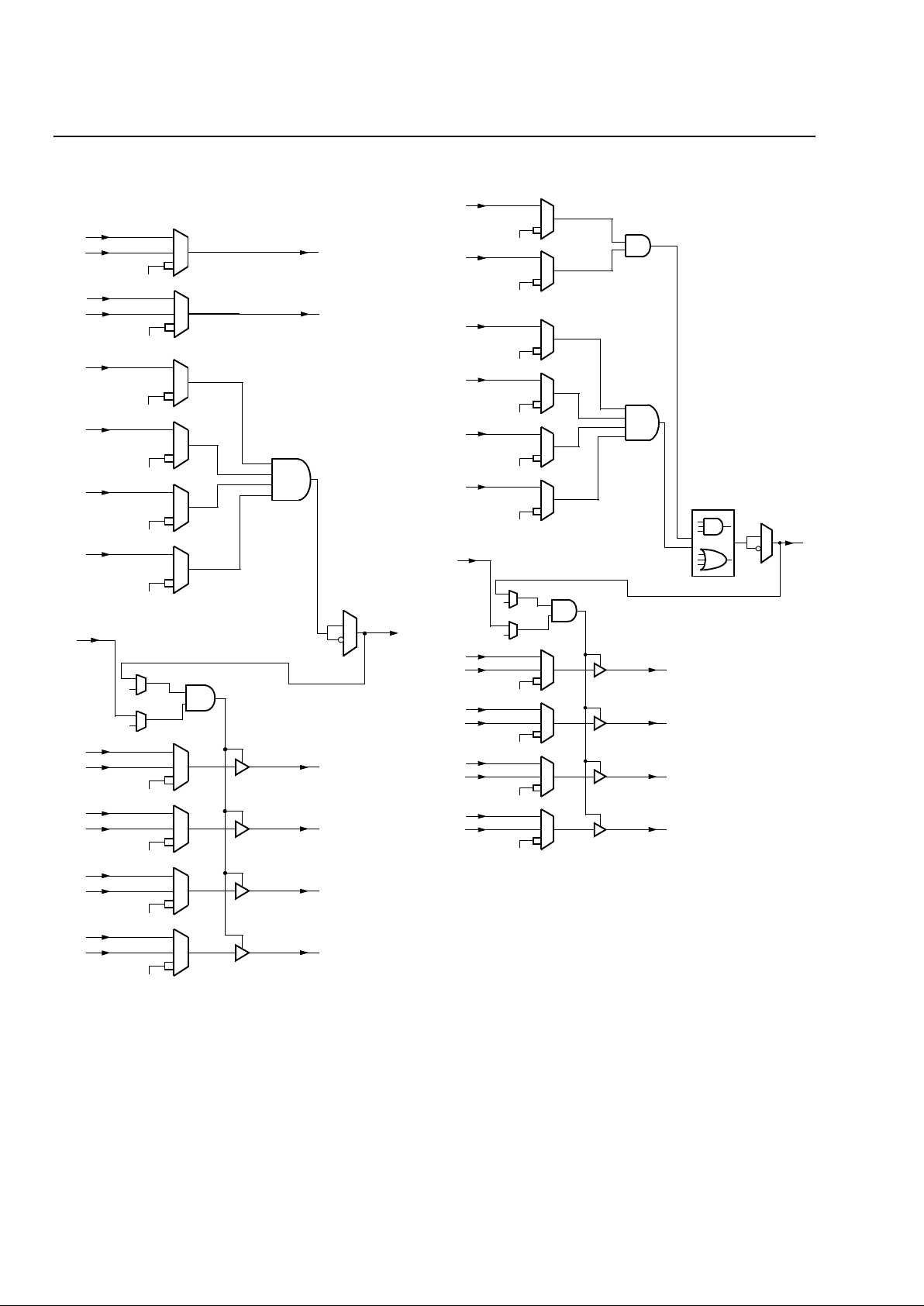
5-5747(F).a
Figure 17. Buffer-Decoder-Buffer Mode
5-5750(F).a
Figure 18. Buffer-Decoder-Decoder Mode
TRI
DEC
1
1
SOUT08
SIN8
I8
LOGIC 1 OR 0
SOUT09
SIN9
I9
LOGIC 1 OR 0
SIN7
LOGIC 1 OR 0
SIN6
LOGIC 1 OR 0
SIN5
LOGIC 1 OR 0
SIN4
LOGIC 1 OR 0
SOUT03
SIN3
I3
LOGIC 1 OR 0
SOUT02
SIN2
I2
LOGIC 1 OR 0
SOUT01
SIN1
I1
LOGIC 1 OR 0
SOUT00
SIN0
I0
LOGIC 1 OR 0
IF LOW, THEN 3-STATE BUFFERS ARE HIGH Z.
DEC
TRI
1
1
SIN7
LOGIC 1 OR 0
SIN6
LOGIC 1 OR 0
SIN5
LOGIC 1 OR 0
SIN4
LOGIC 1 OR 0
SOUT03
SIN3
I3
LOGIC 1 OR 0
SOUT02
SIN2
I2
LOGIC 1 OR 0
SOUT01
SIN1
I1
LOGIC 1 OR 0
SOUT00
SIN0
I0
LOGIC 1 OR 0
SIN9
LOGIC 1 OR 0
SIN8
LOGIC 1 OR 0
Lucent Technologies Inc. 25
Preliminary Data Sheet
December 2000
ORCA Series 4 FPGAs
Programmable Logic Cells
(continued)
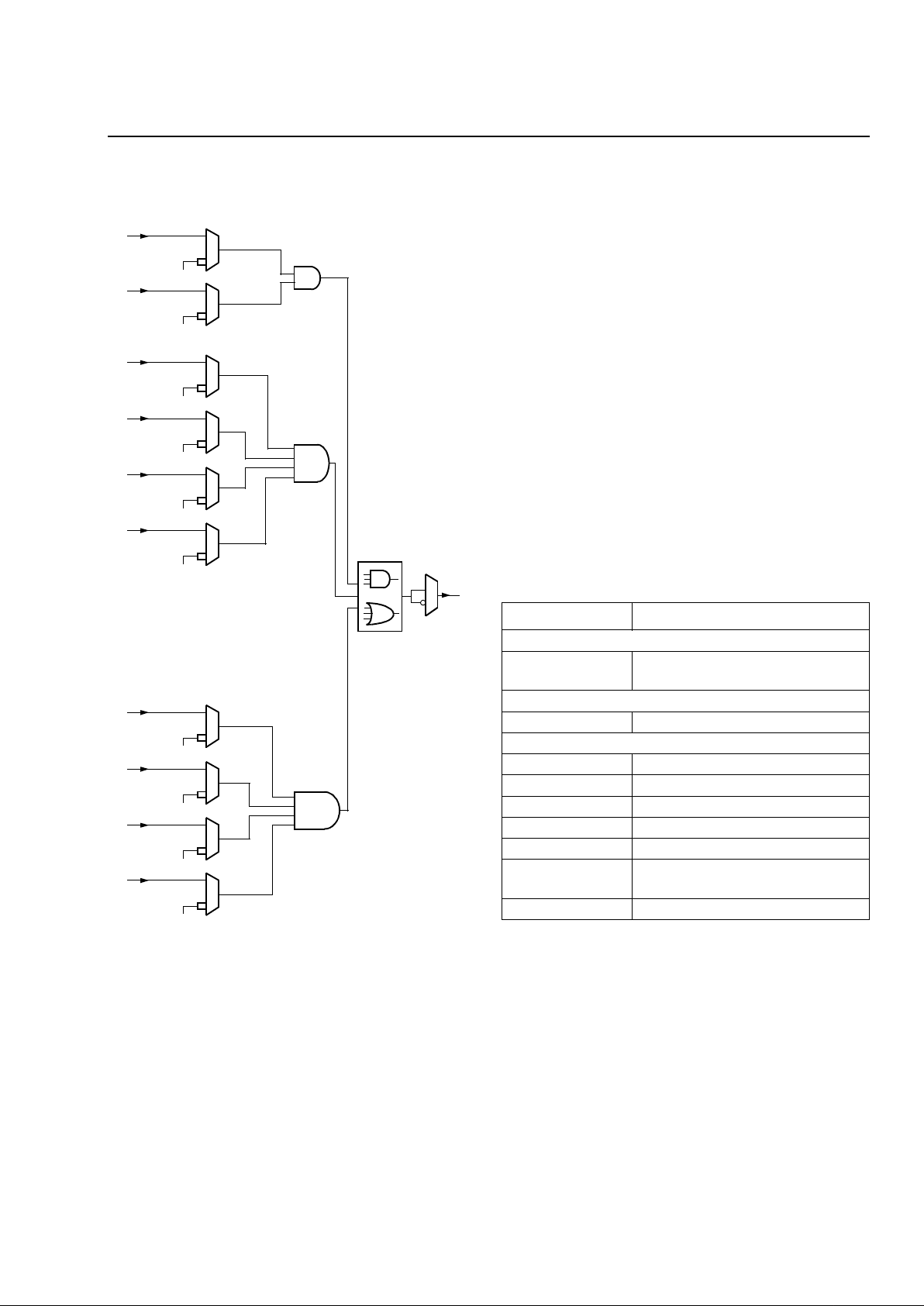
5-5748(F)
Figure 19. Decoder Mode
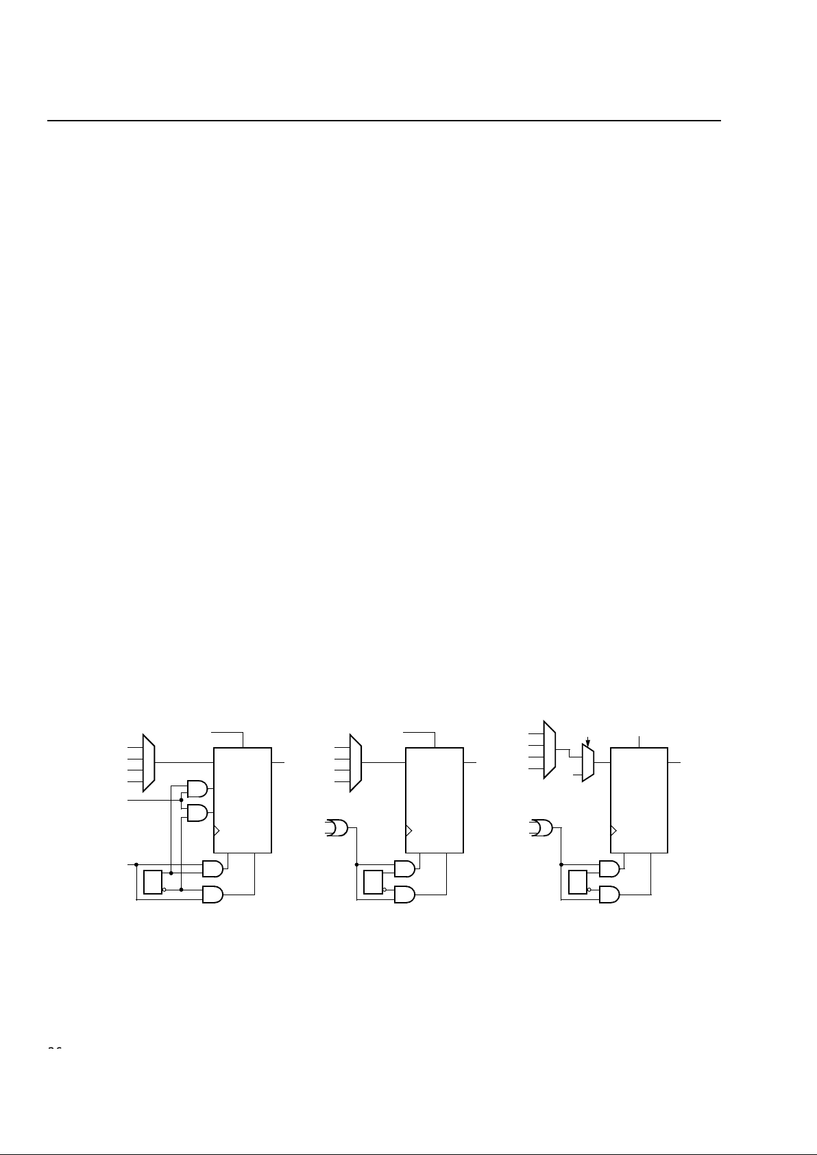
PLC Latches/Flip-Flops
The eight general-purpose latches/FFs in the PFU can
be used in a variety of configurations. In some cases,
the configuration options apply to all eight latches/FFs
in the PFU and some apply to the latches/FFs on a nibblewide basis where the ninth FF is considered independently. For other options, each latch/FF is
independently programmable. In addition, the ninth FF
can be used for a variety of functions.
Table 7 summarizes these latch/FF options. The
latches/FFs can be configured as either positive- or
negative-level sensitive latches, or positive or negative
edge-triggered FFs (the ninth register can only be a
FF). All latches/FFs in a given nibble of a PFU share
the same clock, and the clock to these latches/FFs can
be inverted. The input into each latch/FF is from either
the corresponding LUT output (F[7:0]) or the direct data
input (DIN[7:0]). The latch/FF input can also be tied to
logic 1 or to logic 0, which is the default.
Table 7. Configuration RAM Controlled Latch/
Flip-Flop Operation
* Not available for FF[8].
Each PFU has two independent programmable clocks,
clock enable CE[1:0], local set/reset LSR[1:0], and
front-end data selects SEL[1:0]. When CE is disabled,
each latch/FF retains its previous value when clocked.
The clock enable, LSR, and SEL inputs can be inverted
to be active-low.
DEC
SIN7
LOGIC 1 OR 0
SIN6
LOGIC 1 OR 0
SIN5
LOGIC 1 OR 0
SIN4
LOGIC 1 OR 0
SIN9
LOGIC 1 OR 0
SIN8
LOGIC 1 OR 0
SIN3
LOGIC 1 OR 0
SIN1
LOGIC 1 OR 0
SIN2
LOGIC 1 OR 0
SIN0
LOGIC 1 OR 0
Function Options
Common to All Latches/FFs in PFU
Enable GSRN GSRN enabled or has no effect on
PFU latches/FFs.
Set Individually in Each Latch/FF in PFU
Set/Reset Mode Set or reset.
By Group (Latch/FF[3:0], Latch/FF[7:4], and FF[8])
Clock Enable CE or none.
LSR Control LSR or none.
Clock Polarity Noninverted or inverted.
Latch/FF Mode Latch or FF.
LSR Operation Asynchronous or synchronous.
Front-end Select* Direct (DIN[7:0]) or from LUT
(F[7:0]).
LSR Priority Either LSR or CE has priority.
2626 Lucent Technologies Inc.
Preliminary Data Sheet
December 2000
ORCA Series 4 FPGAs
Programmable Logic Cells
(continued)
The set/reset operation of the latch/FF is controlled by
two parameters: reset mode and set/reset value. When
the GSRN and local set/reset (LSR) signals are not
asserted, the latch/FF operates normally. The reset
mode is used to select a synchronous or asynchronous
LSR operation. If synchronous, LSR has the option to
be enabled only if clock enable (CE) is active or for LSR
to have priority over the clock enable input, thereby setting/resetting the FF independent of the state of the
clock enable. The clock enable is supported on FFs,
not latches. It is implemented by using a 2-input multiplexer on the FF input, with one input being the previous state of the FF and the other input being the new
data applied to the FF. The select of this 2-input multiplexer is clock enable (CE), which selects either the
new data or the previous state. When the clock enable
is inactive, the FF output does not change when the
clock edge arrives.
The GSRN signal is only asynchronous, and it sets/
resets all latches/FFs in the FPGA based upon the set/
reset configuration bit for each latch/FF. The set/reset
value determines whether GSRN and LSR are set or
reset inputs. The set/reset value is independent for
each latch/FF. An option is available to disable the
GSRN function per PFU after initial device configuration.
The latch/FF can be configured to have a data frontend select. Two data inputs are possible in the frontend select mode, with the SEL signal used to select
which data input is used. The data input into each
latch/FF is from the output of its associated LUT,
F[7:0], or direct from DIN[7:0], bypassing the LUT. In
the front-end data select mode, both signals are available to the latches/FFs.
If either or both of these inputs is unused or is unavailable, the latch/FF data input can be tied to a logic 0 or
logic 1 instead (the default is logic 0).
The latches/FFs can be configured in three basic
modes:
■
Local synchronous set/reset: the input into the PFU’s
LSR port is used to synchronously set or reset each
latch/FF.
■
Local asynchronous set/reset: the input into LSR
asynchronously sets or resets each latch/FF.
■
Latch/FF with front-end select, LSR either synchronous or asynchronous: the data select signal selects
the input into the latches/FFs between the LUT output and direct data in.
For all three modes, each latch/FF can be independently programmed as either set or reset. Figure 20
provides the logic functionality of the front-end select,
global set/reset, and local set/reset operations.
The ninth PFU FF, which is generally associated with
registering the carry-out signal in ripple mode functions, can be used as a general-purpose FF. It is only
an FF and is not capable of being configured as a latch.
Because the ninth FF is not associated with an LUT,
there is no front-end data select. The data input to the
ninth FF is limited to the CIN input, logic 1, logic 0, or
the carry-out in ripple and half-logic modes.
5-9737(F).a
Key: CD = configuration data.
Figure 20. Latch/FF Set/Reset Configurations
CE
CE
DQ
S_SET
S_RESET
CLK
SET RESET
F
DIN
LOGIC 1
LOGIC 0
LSR
CD
GSRN
CE
CE
DQ
CLK
SET RESET
F
DIN
LOGIC 1
LOGIC 0
CD
GSRN
LSR
CE
CE
DQ
CLK
SET RESET
F
DIN
LOGIC 1
LOGIC 0
CD
GSRN
LSR
DIN
SEL

Lucent Technologies Inc. 27
Preliminary Data Sheet
December 2000
ORCA Series 4 FPGAs
Embedded Block RAM
The ORCA Series 4 devices complement the distributed PFU RAM with large blocks of memory macrocells. The memory is available in 512 words by 18 bits/
word blocks with two write and two read ports. Two byte
lane enables also operate with quad-port functionality.
Additional logic has been incorporated for FIFO, multiplier, and CAM implementations. The RAM blocks are
organized along the PLC rows and are added in proportion to the FPGA array sizes as shown in Table 8.
The contents of the RAM blocks may be optionally initialized during FPGA configuration.
Table 8. ORCA Series 4— Available Embedded
Block RAM
Each highly flexible 512 x 18 (quad-port, two read/two
write) RAM block can be programmed by the user to
meet their particular function. Each of the EBR configurations use the physical signals as shown in
Table 9. Quad-port addressing permits simultaneous
read and write operations.
The EBR ports are written synchronously on the positive edge of CKW . Synchronous read operations use
the positive edge of CKR. Options are available to use
synchronous read address registers and read output
registers, or to bypass these registers and have the
RAM read operate asynchronously.
EBR Features
Quad-Port Modes (Two Read/Two Write)
■
512 x 18 with optional built-in arbitration between
write ports.
■
1024 x 18 built on two blocks with built-in decode
logic for simplified implementation and increased
speed.
Dual-Port Modes (One Read/One Write)
■
One 256 x 36.
■
One 1K x 9.
■
Two 512 x 9 built in one EBR with two separate read,
write clocks and enables for independent operation.
■
Two RAMs with a user customized number of words
whose sum is 512 (or less) by 18.
The joining of RAM blocks is supported to create wider
and deeper memories. The adjacent routing interface
provided by the CIBs allow the cascading of blocks
together with minimal penalties due to routing delays.
FIFO Modes
FIFOs can be configured to 256, 512, or 1K depths and
36, 18, or 9 widths respectively or two-512 x 9 but also
can be expanded using multiple blocks. FIFO works
synchronously with the same read and write clock
where the read port can be registered on the output or
not registered. It can also be optionally configured
asynchronously with different read and write clocks.
Integrated flags allow the user the ability to fully utilize
the EBR for FIFO, without the need to dedicate an
address for providing distinct full/empty status. There
are four programmable flags provided for each FIFO:
Empty, partially empty, full, and partially full FIFO status. The partially empty and partially full flags are programmable with the flexibility to program the flags to
any value from the full or empty threshold. The programmed values can be set to a fixed value through the
bit stream, or a dynamic value can be controlled by
input pins of the EBR FIFO.
Multiplier Modes
The ORCA EBR supports two variations of multiplier
functions. Constant coefficient MULTIPLY [KCM] mode
will produce a 24-bit output of a fixed 8-bit constant
multiply of a 16-bit number or a fixed 16-bit constant
multiply of an 8-bit number. This KCM multiplies a constant times a 16- or 8-bit number and produces a product as a 24-bit result. The coefficient and multiplication
tables are stored in memory . Both the input and outputs
can be configured to be registered for pipelining. Both
write ports are available during MULTIPLY mode so
that the user logic can update and modify the coefficients for dynamic coefficient updates.
An 8 x 8 MULTIPLY mode is configurable to either a
pipelined or combinatorial multiplier function of two
8-bit numbers. Two 8-bit operands are multiplied to
yield a 16-bit product. The input and outputs can be
registered in pipeline mode.
Device Number of
Blocks
Number of
EBR Bits
OR4E2 8 74K
OR4E4 12 111K
OR4E6 16 148K
OR4E10 20 185K
OR4E14 24 222K

2828 Lucent Technologies Inc.
Preliminary Data Sheet
December 2000
ORCA Series 4 FPGAs
Embedded Block RAM
(continued)
CAM Mode
The CAM block is a content address memory that provides fast address searches by receiving data input
and returning addresses that contain the data. Implemented in each EBR are two 16-word x 8-bit CAM
function blocks.
The CAM has three modes: single match, multiple
match, and clear, which are all achieved in one clock
cycle. In single-match mode, an 8-bit data input is internally decoded and reports a match when data is
present in a particular RAM address. Its result is
reported by a corresponding single address bit. In multiple match, the same occurs with the exception of multiple address lines report the match. Clear mode is
used to clear the CAM contents in one clock cycle by
erasing all locations.)
Arbitration logic is optionally programmed by the user
to signal occurrences of data collisions as well as to
block both ports from writing at the same time. The
arbitration logic prioritizes PORT1. When utilizing the
arbiter, the signal BUSY indicates data is being written
to PORT1. This BUSY output signals PORT1 activity by
driving a high output. The arbitration default is enabled;
however, the user may disable the arbiter in configuration. If the arbiter is turned off, both ports could be written at the same time and the data would be corrupt. In
this scenario, the BUSY signal will indicate a possible
error.
There is also a user option which dedicates PORT 1 to
communications to the system bus. In this mode, the
user logic only has access to PORT0 and arbitration
logic is enabled. The system bus utilizes the priority
given to it by the arbiter; therefore, the system bus will
always be able to write to the EBR.
Table 9. RAM Signals
Port Signals I/O Function
PORT 0
AR0[#:0] I Address to be read.
AW0[#:0] I Address to be written.
BW0<1:0> I Byte-write enable.
Byte = 8 bits + parity bit.
<1> = bits[17, 15:9] < 0> = bits[16, 7:0]
CKR0 I Positive-edge asynchronous read clock.
CKW0 I Positive-edge synchronous write clock.
CSR0 I Enables read to output. Active-high.
CSW0 I Enables write to occur. Active-high.
D [#:0] I Input data to be written to RAM.
Q [#:0] O Output data of memory contents at referenced ad dres s.
PORT 1
AR1[#:0] I Address to be read.
AW1[#:0] I Address to be written.
BW1<1:0> I Byte-write enable.
Byte = 8 bits + parity bit.
<1> = bits[17, 15:9] < 0> = bits[16, 7:0]
CKR1 I Positive-edge asynchronous read clock.
CKW1 I Positive-edge synchronous write clock.
CSR1 I Enables read to output. Active-high.
CSW1 I Enables write to occur. Active-high.
D [#:0] I Input data to be written to RAM.
Q [#:0] O Output data of memory contents at referenced ad dres s.
Control
BUSY O PORT1 writing. Active-high.
RESET I Data output registers cleared. Memory conte nt s unaf fected. Active-low.
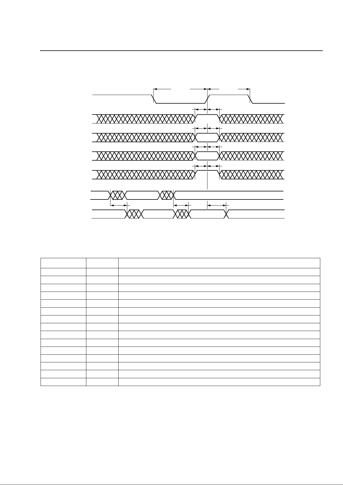
Lucent Technologies Inc. 29
Preliminary Data Sheet
December 2000
ORCA Series 4 FPGAs
Embedded Block RAM
(continued)
0308 (F)
Figure 21. EBR Read and Write Cycles with Write Through
Table 10. FIFO Signals
Port Signals I/O Function
AR(1:0)[9:0] I Programs FIFO flags. Used for partially empty flag size.
AW(1:0)[9:0] I Programs FIFO flags. Used for partially full flag size.
FF O Full flag.
PFF O Partially full flag.
PEF O Partially empty flag.
EF O Empty flag.
D0[17:0] I Data inputs for all configurations.
D1[17:0] I Data inputs for 256 x 36 configurations only.
CKW[0:1] I Positive-edge write port clock. Port 1 only used for 256 x 36 configurations.
CKR[0:1] I Positive-edge read port clock. Port 1 only used for 256 x 36 configurations.
CSW[1:0] I Active-high write enable. P ort 1 only used for 256 x 36 configurations.
CSR[1:0] I Active-high read enable. Port 1 only used for 256 x 36 configurations.
RESET I Active-low. Resets FIFO pointers.
Q0[17:0] O Data outputs for all configurations.
Q1[17:0] O Data outputs for 256 x 36 configurations.
CKWPHCKWPL
CSWSU CSWH
AWH
DSU DH
BWSU BWH
AWSU
CKWQAQAQH
abcd
bca
d
c
CKW
CSW
AW
D
BW
AR
Q

30 Lucent Technologies Inc.
Preliminary Data Sheet
December 2000
ORCA Series 4 FPGAs
Embedded Block RAM
(continued)
Table 11. Constant Multiplier Signals
Table 12. 8 x 8 Multiplier Signals
Table 13. CAM Signals
Port Signals I/O Function
AR0[15:0] I Data input—operand.
AW(1:0)[8:0] I Address bits.
D(1:0)[17:0] I Data inputs to load memory or change coefficient.
CKW[0:1] I Pos iti ve-edge wr it e port clock.
CKR[0:1] I Positive-edge read port clock. Used for synchronous multiply mode.
CSW[1:0] I Activ e-high write enable.
CSR[1:0] I Active-high read enable.
Q[23:0] O Data outputs—product result.
Port Signals I/O Function
AR0[7:0] I Data input—multiplicand.
AR1[7:0] I Data input—multiplier.
AW(1:0)[8:0] I Address bits for memory.
D(1:0)[17:0] I Data inputs to load memory.
CKW[0:1] I Pos iti ve-edge wr it e port clock.
CKR[0:1] I Positive-edge read port clock. Used for synchronous multiply mode.
CSW[1:0] I Activ e-high write enable.
CSR[1:0] I Active-high enables. For enabling address registers.
BW(1:0)[1:0] I Byte-lane write for loading memory.
Q[15:0] O Data outputs—product.
Port Signals I/O Function
AR(1:0)[7:0] I Data match.
AW(1:0)[8:0] I Data write.
D(1:0)[17] I Clear data active-high.
D(1:0)[16] I Sin gle match active-high.
D(1:0)[3:0] I CAM address for data write.
CSW[1:0] I Active-high write enable. Enable for CAM data write.
CSR[1:0] I Active-high enable data registers. Enable for CAM data registers.
Q(1:0)15:0] O Decoded data outputs. 1 corresponds to a data match at that address location.
 Loading...