

AGERE LUCW3030ACA, LUCW3030ACA-DB Datasheet
Data Sheet
April 1999
W3030 3 V Dual-Mode IF Cellular Receiver
Features
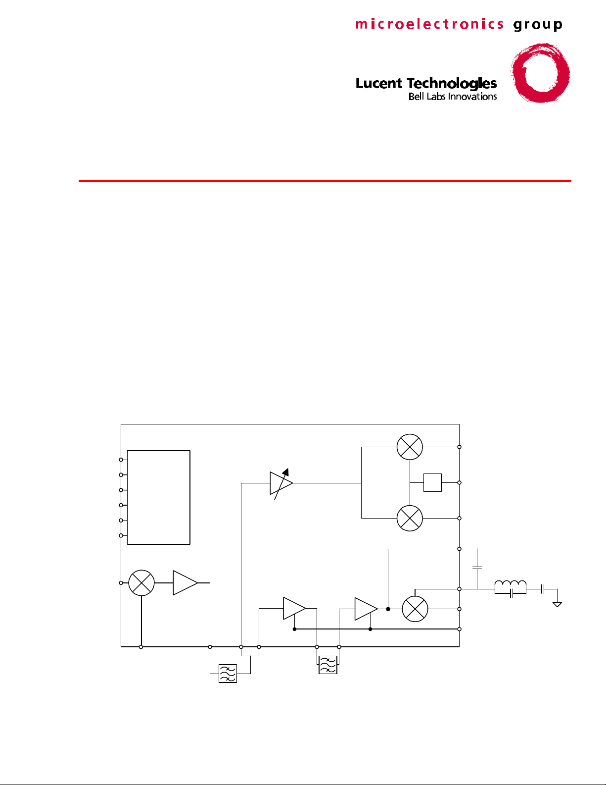
n Proven double conversion architecture:
First IF capability: 10 MHz to over 1000
MHz
Second IF capability: 0.2 MHz to 2.0 MHz
n Dual second IF amplifiers and demodulators:
Analog-mode limiting amplifier and FM
quadrature detector
Digital-mode linear AGC amplifiers with
dual-mixer I & Q quadrature demodulator
n Accurate, onboard local oscillator phase splitter
for digital quadrature demodulator
n Four enable/powerdown modes, selectable from
two digital control pins, allow operation with
minimal supply current
VCC
GND
ENBA
ENBD
VCM
AGC
LOGIC AND
BIAS
CONTROL
DIGITAL SECTION
VARIABLE GAIN
n Low supply current
n Analog received signal strength indicator (RSSI)
available
n Analog AGC for digital-mode IF amplifiers
n Over 100 dB combined voltage gain
Applications
n IS-136 (North American dual-mode) cellular
radio portable and mobile terminals
n Cellular radio base stations
n Digital satellite communications
n Multisymbol signaling receivers
I
÷4
CLK
Q
IF INPUT
ANALOG SECTION
AUDIO
RSSI
LO
Figure 1. General Block Diagram

Data Sheet
W3030 3 V Dual-Mode IF Cellular Receiver April 1999
Table of Contents
Features............................................................................................................................................................... 1
Applications .........................................................................................................................................................1
Description...........................................................................................................................................................3
Pin Information.....................................................................................................................................................5
Absolute Maximum Ratings.................................................................................................................................. 7
Handling Precautions...........................................................................................................................................7
Operating Ranges................................................................................................................................................8
Electrical Specifications ....................................................................................................................................... 8
RSSI..................................................................................................................................................................11
Quadrature Detector........................................................................................................................................... 11
Quad Tank S-Curves......................................................................................................................................12
Test Circuit Diagram ..........................................................................................................................................14
Characteristic Curves......................................................................................................................................... 15
Outline Diagram................................................................................................................................................. 20
32-Pin TQFP ......................................................................................................................................................20
Manufacturing Information ................................................................................................................................. 21
Ordering Information..........................................................................................................................................21
Lucent Technologies Inc.2

Data Sheet
April 1999 W3030 3 V Dual-Mode IF Cellular Receiver
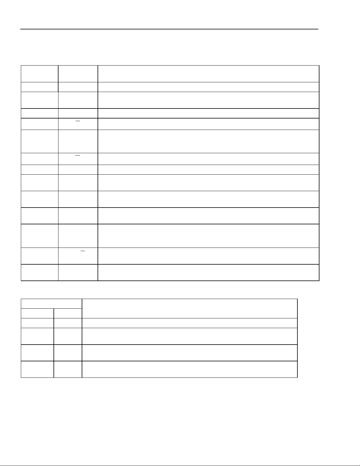
Description
The W3030 is a monolithic integrated circuit that
provides most of the receive path functions required
to meet the IS-136 (and IS-54) standard. The W3030
converts FM or digitally modulated IF carriers up to
200 MHz and provides required IF gain and separate
baseband detectors for the two modulation modes.
The W3030 is organized into three subfunctions (see
Figure 2):
1. First IF mixer/amplifier
2. Analog second IF
3. Digital second IF sections
(Note that the electrical specification tables
correspond to each subfunction.)
Each section has a buffered output to allow for
external filtering, which also provides flexibility in
system architecture selection. The first IF mixer
section provides 30 dB of fixed voltage conversion
gain (power gain = 17 dB). The first IF mixer also
performs down-conversion to the 0.2 MHz—2.0 MHz
range, which allows the use of inexpensive ceramic
filters at two points in the signal path. In the second IF
section, the signal path may be split between two
parallel amplifier/demodulator sections. In the analog
second IF, there is a 40 dB amplifier followed by a
60 dB hard-limiting amplifier and an FM quadrature
detector (noncoherent discriminator). The signal path
between the 40 dB and 60 dB amplifier stages is
brought off-chip for external filtering purposes. In
digital mode, an AGC amplifier provides gain between
10 dB and 80 dB. The digital signal is demodulated in
double-balanced mixers that are fed with an external
local oscillator (LO) signal. The external LO passes
through a divide-by-four counter to provide the final IF
LO frequency. This architecture greatly reduces the
possibility of feedback of the external LO signal to the
IF input, which would cause dc offsets at the I & Q
outputs. This circuit also provides a 90° phase shift of
the LO that is independent of duty cycle. The resulting
I & Q differential pairs can be level-shifted using the
VCM input pin, providing flexibility in interfacing to
digital processing ICs.
A pair of logic inputs allows the device to be put into a
powerdown mode and one of two partially enabled
modes (analog or digital only), or a fully enabled
mode, allowing the use of analog RSSI while in digital
receive mode.
Lucent Technologies Inc. 3

Data Sheet
IF
IF
IF
W3030 3 V Dual-Mode IF Cellular Receiver April 1999
Description (continued)
RSSI
AUDIO
QUAD
IFAOUT
IFAACG
IFAIN
1
FM
DEMOD &
RSSI
2
3
49 kΩ
4
5
1 kΩ
6
GND2
32 31 30 29 28 27 26 25
IFDIN
IFDIN
50 kΩ
ANALOG SECOND
IFDACG
AGC AMP I/Q DEMODULATOR
IF LIMITER
VCM
2 kΩ
AGC
50 kΩ
48 kΩ
FIRST IF MIXER/AMPLIFIER
10 MHz—1000 MHz
I
I
÷
4
24
23
22
21
20
19
CLK
Q
Q
ENBA
ENBD
IF1IN
IFAIN
VCC2
7
8
1 kΩ
9 10 11 12 13 14 15 16
2OUT
50 kΩ
48 kΩ
2ACG
SECOND IF AMP
0.2 MHz—2.0 MHz
2 kΩ
IF2IN
1 kΩ
IF2IN
GND1
1OUT
IF1LO
IF1LO
18
17
IF1IN
VCC1
Figure 2. Detailed Block Diagram with Pinout
Lucent Technologies Inc.4

Data Sheet
April 1999 W3030 3 V Dual-Mode IF Cellular Receiver
Pin Information
Table 1. Pin Descriptions
Pin
Number
1 RSSI
2 AUDIO
3 QUAD
4 IFAOUT
5 IFAACG
6 IFAIN
7
8 VCC2
9 IF2OUT
10 IF2ACG
11 IF2IN
12
13 GND1
14 IF1OUT
15
16 IF1LO
17 VCC1
18
19 IF1IN
Pin Name Pin Description
IFAIN
IF2IN
IF1LO
IF1IN
Received Signal Strength Indicator. Provides logarithmic (dB-linear) dc output
voltage.
Audio Output. Audio output of FM detector.
Quad Input. Input to FM detector from parallel LC quad coil.
Analog Output. Output of analog section limiting amplifiers; couple to quad coil
and pin 3 (QUAD) with 10 pF capacitor.
Analog Signal Ground. Signal ground for analog section limiting amplifier;
connect to ground with 0.1 µF capacitor.
Analog Mode Limiter Input. Differential input to analog IF limiting amplifier; to
be directly coupled to dielectric sources such as ceramic filters. Pin 6 is
approximately 1 kΩ with pin 5 ac-grounded.
Analog Mode Limiter Input (Inverting). Differential input to analog IF limiting
amplifier. To be ac-grounded.
Second IF Power Supply. Positive power supply connection for both analog
and digital second IF amplifiers and demodulators.
Second IF Output. Output of 40 dB second IF amplifier; directly couple to
dielectric loads such as ceramic filters. Includes internal 1 kΩ termination
resistor.
Second IF Signal Ground. Signal ground for 40 dB second IF amplifier;
connect to ground with 0.1 µF capacitor.
Second IF Input. Differential input to 40 dB second IF amplifier; to be directly
coupled to dielectric sources such as ceramic filters. Pin 11 is approximately
2 kΩ with pin 10 ac-grounded.
Second IF Input (Inverting). Differential input to 40 dB second IF amplifier. To
be ac-grounded.
First IF Mixer Ground. Power supply (dc) ground for first IF mixer section.
First IF Mixer Output. Output of first IF mixer/amplifier section; to be directly
coupled to dielectric loads such as ceramic filters. Includes internal 1 kΩ
termination resistor.
First IF Mixer Logical Input (Inverting). Differential input to first IF mixer local
oscillator; to be capacitively coupled to sources with a dc level offset.
First IF Mixer Logical Input. Differential input to first IF mixer local oscillator.
To be ac-grounded.
First IF Mixer Power Supply. Positive power supply connection for first IF
mixer/amplifier section.
First IF Mixer Input (Inverting). Differential input to first IF mixer/amplifier
section; to be ac-coupled to ground or source.
First IF Mixer Input. Differential input to first IF mixer/amplifier section.
Lucent Technologies Inc. 5
Data Sheet
W3030 3 V Dual-Mode IF Cellular Receiver April 1999
Pin Information (continued)
Table 1. Pin Descriptions (continued)
Pin
Number
20 ENBD
21 ENBA
22 Q
23
24 CLK
25
26 I
27 AGC
28 VCM
29 IFDACG
30 IFDIN
31
32 GND2
Pin Name Pin Description
Q
I
IFDIN
Enable Digital Mode. Positive logic enable connection for digital mode operation.
Enable Analog Mode. Positive logic enable connection for analog mode
operation.
Q Output. Differential output from Q mixer of quadrature demodulator.
Q Output (Inverting). Differential output from Q mixer of quadrature demodulator.
Clock Input. Local oscillator (clock) input to quadrature demodulator phase shifter;
to be capacitively coupled. Input frequency must be four times second IF center
frequency.
I Output (Inverting). Differential output from I mixer of quadrature demodulator.
I Output. Differential output from I mixer of quadrature demodulator.
Automatic Gain Control. AGC control input; to be connected to dc source of
0.25 V—1.55 V.
Common-Mode Voltage. Common-mode voltage dc offset set point for I & Q
interface, typically VCC/2.
Digital Signal Ground. Signal ground for digital section limiting amplifier; connect
to ground with 0.1 µF capacitor.
Digital Second IF Input. Differential input to digital section AGC amplifier; to be
directly coupled to dielectric sources such as ceramic filters. Pin 30 is
approximately 2 kΩ with pin 29 ac-grounded.
Digital Second IF Input (Inverting). Differential input to digital section AGC
amplifier. To be ac-grounded.
Second IF Ground. Power supply ground for both analog and digital second IF
amplifier and demodulator sections.
Table 2. Digital Control Pin Truth Table
Control Pin Mode/Function
ENBA ENBD
LOW LOW
LOW HIGH
HIGH LOW
HIGH HIGH
All Sleep. All receive circuits powered down, supply current <10 µA.
Digital Receive. First IF mixing stage, AGC amp and I/Q quadrature
demodulators active.
Analog/FM Receive. First IF mixing stage, 40 dB IF amp, 60 dB limiting amp,
RSSI, and FM detector active.
All Active. All receive circuits functional, e.g., digital mode I & Q demodulator
used with analog RSSI.
Lucent Technologies Inc.6
Data Sheet
April 1999 W3030 3 V Dual-Mode IF Cellular Receiver
Absolute Maximum Ratings
Stresses in excess of the absolute maximum ratings can cause permanent damage to the device. These are
absolute stress ratings only. Functional operation of the device is not implied at these or any other conditions in
excess of those given in the operations sections of the data sheet. Exposure to absolute maximum ratings for
extended periods can adversely affect device reliability.
Parameter Min Max Unit
Ambient Operating Temperature –35 100 °C
Storage Temperature –65 150 °C
Lead Temperature (soldering, 10 s) — 300 °C
Positive Supply Voltage 0 4.5 Vdc
Power Dissipation — 650 mW
Output Current (continuous) — 160 mA
ac Peak-to-peak Input Voltage 0 VCC Vdc
Enable Input Voltage –0.3 VCC + 0.4 Vdc
VCM, AGC Input Voltage –0.3 VCC + 0.4 Vdc
Handling Precautions
Although protection circuitry has been designed into this device, proper precautions should be taken to avoid
exposure to electrostatic discharge (ESD) during handling and mounting. Lucent Technologies Microelectronics
Group employs a human-body model (HBM) and a charged-device model (CDM) for ESD-susceptibility testing
and protection design evaluation. ESD voltage thresholds are dependent on the circuit parameters used to define
the model. No industry-wide standard has been adopted for CDM. However, a standard HBM (resistance =
1500 Ω, capacitance = 100 pF) is widely used and, therefore, can be used for comparison purposes. The HBM
ESD threshold presented here was obtained by using these circuit parameters:
W3030 ESD Threshold Voltage
ESD Model Rating
HBM
CDM
≥1500 V
≥1500 V
Lucent Technologies Inc. 7
 Loading...