

AGERE LUCW3020CCS-DB, LUCW3020CCS Datasheet
Advance Data Sheet
December 1999
W3020 GSM Multiband RF Transceiver
Features
n 2.7 V operation, low power consumption
n Integrated receive, transmit, and synthesizer
functions
n IF frequency and transmit offset frequency
generated from the same LO
n Integrated dual LNAs and mixers
n Minimizes PCB design work between systems
n Surface-mount, 64-pin TQFPT package
GSM1800/1900
IF
270 MHz
GSM900
900: 925 MHz—960 MHz
1800: 1805 MHz—1880 MHz
1900: 1930 MHz—1990 MHz
900: 880 MHz—915 MHz
1800: 1710 MHz—1785 MHz
1900: 1850 MHz—1910 MHz
GSM1800/1900
SAW
VCO
900: 1150 MHz—1230 MHz
1800: 1530 MHz—1610 MHz
1900: 1660 MHz—1730 MHz
TX IF
1800/1900: 180 MHz
Applications
n GSM dual-band hand portables:
— GSM900/1800
— GSM900/1900
n GSM single-band hand portables:
— GSM900
— GSM1800
— GSM1900
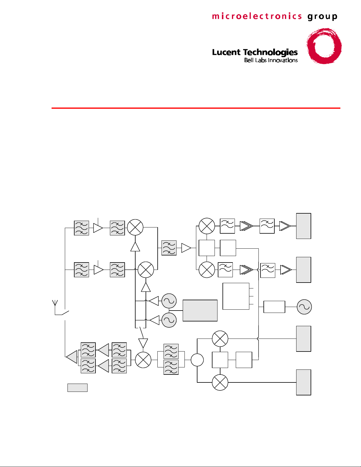
÷
Φ
W3000
FREQUENCY
SYNTHESIZER
2
RF MODE
& AGC
CONTROL
LO2 PLL
ADC
ADC
540 MHz VCO
DAC
RX I
RX Q
TX I
÷
2
÷
3
SWITCHED DIVIDER
DAC
TX Q
PA
GSM900
Note: shaded area is off-chip.
900: 270 MHz
Σ
Φ
Figure 1. W3020 Circuit Block Diagram

Advance Data Sheet
W3020 GSM Multiband RF Transceiver December 1999
Table of Contents
Contents Page Contents Page
Features.................................................................1
Applications ...........................................................1
Description.............................................................4
Detailed Block Diagram......................................5
Pin Information.......................................................6
Absolute Maximum Ratings....................................8
ESD Precautions .................................................... 8
Operating Range .................................................... 8
Digital Serial Inputs................................................ 9
Digital Outputs .......................................................9
Enable Time...........................................................9
Supply Currents ..................................................... 9
LNA......................................................................10
RF Mixer.............................................................. 11
IF/Baseband Amplifier.......................................... 12
Modulator.............................................................15
LO2 Specification................................................. 17
List of Figures
Figure Page Figure Page
Figure 1. W3020 Circuit Block Diagram .................1
Figure 2. IC Block Diagram with Pinout.................. 5
Figure 3. IF Amplifier Gain Steps.........................12
Figure 4. Actual Gain vs. Requested Gain............ 12
Figure 5. IF Strip Balanced Input Matching
Network................................................ 12
Figure 6. IF Filtering Requirements for Wideband
Noise Performance................................16
LO1 Input Buffer Specification ..............................17
Programming Information.....................................18
Serial Bus Timing Information...........................19
The Data Word .................................................20
TR Register.......................................................21
CONFIG Register..............................................26
MAIN Register ..................................................30
Filter Tune and dc Offset Correction Timing......31
Programming Example .........................................33
Application Information .........................................35
S-Parameters....................................................35
Outline Diagram...................................................43
64-Pin TQFPT ..................................................43
Manufacturing Information ....................................44
Evaluation Board Note..........................................44
Ordering Information ............................................44
Figure 7. Diagram of W3020, W3000, and SC1
Interconnection...................................... 18
Figure 8. Serial Bus Timing Diagram....................19
Figure 9. IF and I/Q Gain Distribution (dB)............25
Figure 10. Programming the LO2 Phase Detector
Slope....................................................29
Figure 11. GSM900 Smith Chart Noise Circles.....35
Figure 12. GSM1800 Smith Chart Noise Circles... 36
2 Lucent Technologies Inc.

Advance Data Sheet
December 1999 W3020 GSM Multiband RF Transceiver
List of Tables
Table Page Table Page
Table 1. Pin Assignment.........................................6
Table 2. GSM900 LNA Performance.....................10
Table 3. GSM1800/1900 LNA Performance.......... 10
Table 4. RF Performance: GSM900...................... 11
Table 5. RF Performance: GSM1800/1900...........11
Table 6. IF/Baseband Amplifier Performance .......13
Table 7. Low-Pass Rejection Characteristics.........14
Table 8. Modulator Performance...........................15
Table 9. LO2 Performance ...................................17
Table 10. LO1 Performance..................................17
Table 11. Serial Bus Timing Information............... 19
Table 12. Register Addressing..............................20
Table 13. TR Register........................................... 21
Table 14. B: Band Select......................................22
Table 15. MO[3:1]: Mode Control ..........................23
Table 16. T6: LO2 Disable.................................... 23
Table 17. T5: LO1 Disable.................................... 23
Table 18. T4: Receive IF Duty Cycle Corrector
Disable..................................................23
Table 19. T3: Divide-by-3 Duty Cycle Corrector
Disable..................................................23
Table 20. FTR: LPF Tune Filter Request .............. 24
Table 21. DP: dc Precharge Only .........................24
Table 22. DS: dc Correction Skip ..........................24
Table 23. T2: TX IF LO Division Select Switch .....24
Table 24. T1: TX IF LO Divide-by-6 Select ........... 24
Table 25. T0: TX IF Duty Cycle Corrector Disable.24
Table 26. G[0:6]: Digital Gain Control...................25
Table 27. CONFIG Register.................................. 26
Table 28. C10: LO2 PLL Enable ........................... 27
Table 29. OLD: Overload Output Disable.............. 27
Table 30. C9: RF Mixer On During Settling ...........27
Table 31. VO: LO1 Buffer Mode ...........................27
Table 32. C8: LO2 Charge Pump Off ....................27
Table 33. LD2: Lock Detect Enable....................... 28
Table 34. C7: dc Coarse/Fine Correction ............. 28
Table 35. C6: Filter Tune Disable......................... 28
Table 36. C5: dc Correction Disable ..................... 28
Table 37. C4: Low-Pass Filter Bandwidth............. 28
Table 38. C3: Receive LO1 Buffer Mode During dc
Calibration............................................ 29
Table 39. C2: LNA Mode During dc Calibration.... 29
Table 40. C1: 540 MHz LO2 Phase Detector
Polarity................................................. 29
Table 41. DT[2:0]: dc Correction Time ................. 30
Table 42. RS: Reset Bit Content .......................... 30
Table 43. Initialize CONFIG Register
(Reset W3020)..................................... 33
Table 44. Initialize TR Register............................ 33
Table 45. Settle PLL to GSM1800 Band for Receive
Mode (W3020/W3000)......................... 33
Table 46. Perform Receive (W3020).................... 34
Table 47. Settle PLL in GSM1800 Band for
Transmit Mode (W3020/W3000) .......... 34
Table 48. Basic GSM1800 Transmit Burst
(W3020)............................................... 34
Table 49. GSM900 LNA S-Parameters................. 37
Table 50. GSM1800/GSM1900 LNA
S-Parameters....................................... 38
Table 51. Receive IF Amplifier Input
(0 dB Setting)....................................... 39
Table 52. Receive IF Amplifier Input
(32 dB Setting)..................................... 39
Table 53. Transmit Modulator IF Output............... 40
Table 54. Transmit IF Input to Up-Conversion
Mixer .................................................... 41
Table 55. Transmit RF Output from Up-Conversion
Mixer .................................................... 42
Lucent Technologies Inc. 3

Advance Data Sheet
W3020 GSM Multiband RF Transceiver December 1999
Description The W3020 is a highly integrated GSM transceiver
designed to operate in dual-band handsets or in
single-band handsets operating at 900, 1800, and
1900 MHz frequency bands (1900 MHz performance
is not verified in production). The IC architecture
allows the RF designer to provide solutions for three
different frequency bands with very few PCB changes,
thereby providing faster time to market and reduced
development time.
The W3020 RF transceiver and W3000 PLL have
been designed in conjunction with the SC1 (radio
interface and DSP) to provide a complete GSM
cellular solution. The W3020 interfaces to the W3000
UHF high-performance PLL IC. The W3020, in
combination with the W3000, provides the transmitter,
receiver, and frequency synthesizer. Adding a power
amplifier(s), filters, and VCO modules completes the
radio channel.
The baseband modulated signal is applied to the I/Q
double-balanced mixer in a differential manner. The
±45° phase-shifted local oscillator requires no trim to
achieve the required modulation spectral mask. Also,
I/Q input signals require no dc offset calibration to
achieve high phase accuracy signal. The IF signal
outputs from the I/Q mixers are summed and brought
out to an external filter that reduces the noise that
could be intermodulated into the receive band. This
signal is then applied to the low noise up-conversion
mixer and brought to the RF output.
The received signal is amplified through the low-noise
amplifier, which, combined with the preceding filter,
dominates the receiver sensitivity. The signal is then
passed through another external filter to attenuate the
image frequency to an acceptable level. The signal
passes through the RF down-conversion mixer to the
IF frequency. It is then filtered by an external surface
acoustic wave (SAW) filter to bring the in-band
blocking signals to an acceptable level. The signal is
amplified in the IF strip of the receiver. The IF strip
contains digital gain control (DGC) amplifiers at both
the IF and baseband frequencies and precision lowpass filters. This allows the signal to be amplified
while in-band blocking signals are removed. The
precision I/Q demodulator splits the signal into its inphase and quadrature signals. The I/Q signals are lowpass filtered and further amplified. The I/Q amplifier
contains integrated dc offset calibration circuitry. The
outputs (I/Q) are fed to the ADC for further signal
processing.
The second local oscillator (LO2), comprising a buffer
for the external voltage-controlled oscillator (VCO)
and a phase-locked loop (PLL), feeds the IF portions
of both the modulator and the receiver. An external
reference source, voltage-controlled crystal oscillator
(VCXO), is divided from 13 MHz to 1 MHz through a
counter. The 1 MHz is called the comparison
frequency. The VCO frequency of 540 MHz is also
divided down to 1 MHz. Both signals are fed into a
phase detector, and the resultant error signal is fed
through an external low-pass filter to the control input
of the VCO.
The RF receive and transmit mixers are driven by two
band-switchable external VCO modules and buffered
internally on the IC. The VCOs are both controlled by
a single W3000 PLL synthesizer and loop filter. Fast
band-locking is achieved using a proprietary scaling
technique integrated in the W3000 PLL.
4 Lucent Technologies Inc.
Advance Data Sheet
December 1999 W3020 GSM Multiband RF Transceiver
Description (continued)
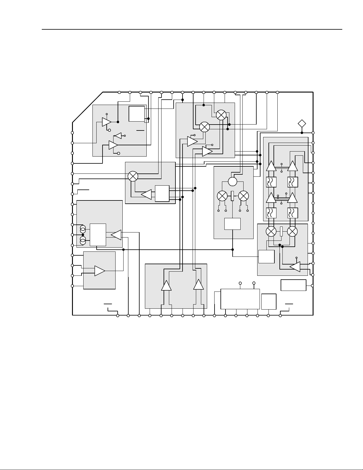
Detailed Block Diagram
EEL2
DLNAI
EEL3
GLNAI
TIFIP
TIFIN
GNDS4
GNDP2
VDDP2
VDDC2
CP2
GNDC2
VDDL2
L2P
L2N
GNDL2
R1
V
GND
TOUT
59
CC
DD
V
58
V
CCM
RF
MIXERS
V
DMIP
57
CCB
MIN
56
V
CCB
GMIP
EER1
54
55
EEGND
V
GND
MODULATOR
TIP TQNTQPTIN
CCB
∑
DIV BY
2 OR 3
TIFOP
53
TIFON
52
V
CC
GND
RMON
51
EEL1
DLNAO
GNDL
GLNAO
TOV
60
61
62
63
64
V
LNA
B
1800
1
2
3
LNA
900
EEL[1:3]
EEL[1:3]
CC
BIAS
GND
s
B
4
TX MIXER
5
6
GND
V
s
CC
7
8
9
MUX
10
11
LO2
PLL
12
13
V
14
15
16
GND
LO2
CC
BUFFER
540 MHz
GSM
1800
GSM
900
G[0:6]
B
DD
V
CONTROL LOGIC/
s s
V
CC
GND
SERIAL BUS
GND
RMOP
50
DIV BY
2
LO2
LOCK
R249
DD
V
4 dB
21 dB
G3
16 dB
4 dB
G1
G5
G6
G2
8 dB
G4
32 dB
TEST
V
GND
s
V
GND
CC
48
GNDS3
RIP
47
RIN
46
45
RQP
RQN
44
43
42
41
40
39
38
37
36
35
34
33
VDDB
GNDB
TQN
TQP
TIN
TIP
VDDI
GNDI
IFIP
IFIN
TEST
CC
32
31
30
29
28
27
26
25
24
23
22
21
20
19
18
17
GNDS1
MCI
MCG
L1
DD
V
DL1P
DL1N
GNDL1
GL1P
GL1N
DD
V
SS
V
CLK
DAT
LAT
LD
GNDS2
Figure 2. IC Block Diagram with Pinout
Lucent Technologies Inc. 5

Advance Data Sheet
W3020 GSM Multiband RF Transceiver December 1999
Pin Information Table 1. Pin Assignment
Pin Symbol Type Pin Description
1 EEL2 Input* LNA Emitter Ground
2 DLNAI Input GSM1800/1900 Band LNA Signal Input
3 EEL3 Input* LNA Emitter Ground
4 GLNAI Input GSM900 Band LNA Signal Input
5 TIFIP Input TX IF Input to Mixer
6 TIFIN Input TX IF Input to Mixer
7 GNDS4 Ground Substrate Ground
8 GNDP2 Ground LO2 PLL Ground
9 VDDP2 Supply LO2 PLL Voltage Supply
10 VDDC2 Supply LO2 Charge Pump Supply
11 CP2 Output Charge Pump LO2 Output
12 GNDC2 Ground LO2 Charge Pump Ground
13 VDDL2 Supply LO2 Buffer Supply
14 L2P Input LO2 Positive Input (540 MHz)
15 L2N Input LO2 Negative Input (on-chip ac ground)
16 GNDL2 Ground LO2 Buffer Ground
17 GNDS1 Ground Substrate Ground
18 MCI Input Master Clock Input
19 MCG Input Master Clock Negative Input (ac ground)
20 VDDL1 Supply VDD Supply for LO1
21 DL1P Input GSM1800/1900 LO1 Positive Input
22 DL1N Input GSM1800/1900 LO1 Negative Input (on-chip ac ground)
23 GNDL1 Ground LO1 Ground
24 GL1P Input GSM900 LO1 Positive Input
25 GL1N Input GSM900 LO1 Negative Input (on-chip ac ground)
26 VDD Supply Voltage Supply for All Digital Circuits
27 VSS Ground Ground for All Digital Circuits
28 CLK Input Clock Input for Serial Bus
29 DAT Input Data Input for Serial Bus
30 LAT Input Latch Enable Input for Serial Bus
31 LD Output LO2 Synthesizer Lock Indicator Output
32 GNDS2 Ground Substrate Ground
*The emitters are considered critical inputs that need to be carefully grounded externally.
6 Lucent Technologies Inc.

Advance Data Sheet
December 1999 W3020 GSM Multiband RF Transceiver
Pin Information (continued)
Table 1. Pin Assignment (continued)
Pin Symbol Type Pin Description
33 Test Output Production Test Output
34 IFIN Input IF DGC Amplifier Input Negative
35 IFIP Input IF DGC Amplifier Input Positive
36 GNDI Ground Ground for IF Amplifier
37 VDDI Supply Voltage Supply IF Amplifier
38 TIP Input TX In-Phase Positive Input
39 TIN Input TX In-Phase Negative Input
40 TQP Input TX Quadrature Positive Input
41 TQN Input TX Quadrature Negative Input
42 GNDB Ground Baseband RX Ground
43 VDDB Supply Baseband RX VDD Supply
44 RQN Output RX Quadrature Phase Negative Output
45 RQP Output RX Quadrature Phase Positive Output
46 RIN Output RX In-Phase Negative Output
47 RIP Output RX In-Phase Positive Output
48 GNDS3 Ground Substrate Ground RF dc Supply
49 VDDR2 Supply RF RX/TX Voltage Supply
50 RMOP Output RX Mixer Output Positive
51 RMON Output RX Mixer Output Negative
52 TIFON Output TX IF Output from Modulator Negative
53 TIFOP Output TX IF Output from Modulator Positive
54 EER1 Input* RX Mixer Emitter Ground
55 GMIP Input GSM900 Mixer Input Positive
56 MIN Input RF Mixer Input Negative (ac ground)
57 DMIP Input GSM1800 Mixer Input Positive
58 VDDR1 Supply RF RX Voltage Supply
59 TOUT Output Transmit Mixer Output
60 TOV Output Transmit Mixer Output
61 GLNAO Output GSM Band LNA Output
62 GNDL Ground LNA Substrate Ground
63 DLNAO Output GSM1800 Band LNA Output
64 EEL1 Input* LNA Emitter Ground
*The emitters are considered critical inputs that need to be carefully grounded externally.
Lucent Technologies Inc. 7
Advance Data Sheet
W3020 GSM Multiband RF Transceiver December 1999
Absolute Maximum Ratings Stresses in excess of the absolute maximum ratings can cause permanent damage to the device. These are
absolute stress ratings only. Functional operation of the device is not implied at these or any other conditions in
excess of those given in the operations sections of this data sheet. Exposure to maximum ratings for extended
periods can adversely affect device reliability.
Parameter Symbol Min Max Unit
Ambient Operating Temperature TA –30 85 °C
Storage Temperature Tstg –65 150 °C
Lead Temperature (soldering, 10 s) — — 300 °C
Positive Supply Voltage VDD 0 4.5 V
Power Dissipation PD — 550 mW
ac Peak-to-Peak Input Voltage Vp-p 0 VDD V
Digital Voltages — 0 VDD V
ESD Precautions Although protection circuitry has been designed into this device, proper precautions should be taken to avoid
exposure to electrostatic discharge (ESD) during handling and mounting. Lucent Technologies Microelectronics
Group employs a human-body model (HBM) and a charged-device model (CDM) for ESD-susceptibility testing
and design evaluation. ESD voltage thresholds are dependent on the circuit parameters used to define the
model. No industry-wide standard has been adopted for CDM. However, a standard HBM (resistance = 1500 Ω,
capacitance = 100 pF) is widely used and, therefore, can be used for comparison purposes. The HBM ESD
threshold presented here was obtained by using these circuit parameters:
Parameter Method Rating Unit
ESD Threshold Voltage HBM 1500 V
ESD Threshold Voltage (corner pins) CDM 1000 V
ESD Threshold Voltage CDM 500 V
Operating Range The device is fully functional within the following operation ranges. No claims of parametric performance are
stated within this range. For parametric performance, refer to the individual specifications and operating
conditions.
Parameter Symbol Min Max Unit
Operating Temperature TA –30 85
Nominal Operating Voltage VDD 2.7 3.6 V
°C
8 Lucent Technologies Inc.
Advance Data Sheet
December 1999 W3020 GSM Multiband RF Transceiver
Digital Serial Inputs
Parameter Symbol Min Max Unit
Logic High Voltage VIH 0.7 * VDD — V
Logic Low Voltage VIL — 0.3 * VDD V
Logic High Current (VIH = 3.0 V) |IIH| — 10
Logic Low Current (VIL = 0.0 V) |IIL| — 10
µA
µA
Clock Input Frequency (VDD = 2.7 V) fCLK — 10 MHz
Digital Outputs
Parameter Symbol Min Max Unit
Logic High Voltage VOH VDD – 0.4 — V
Logic Low Voltage VOL — 0.4 V
Logic High Current (VOH ≥ VDD –
|IOH| 2 — mA
0.4)
Logic Low Current (VOL ≤ 0.4 V)
|IOL| 2 — mA
Enable Time VDD = 2.7 Vdc; TA = 25 °C ± 3 °C.
Parameter Min Typ Max Unit
Logic Powerup/down Time — — 4.0
µs
Supply Currents VDD = 2.7 Vdc; TA = 25 °C ± 3 °C.
System Mode Min Typ Max Unit
Powerdown (VDD = 3.0
— 2 50
µA
Vdc)*
PLL RX Settling — 33 — mA
RX Mode (LNA = ON) — 68 — mA
RX Mode (LNA = OFF) — 64 — mA
PLL TX Settling — 33 — mA
TX Mode — 92 — mA
*This current does not include LO2 charge pump supply current. (See LO2 specification for details.)
Lucent Technologies Inc. 9

Advance Data Sheet
W3020 GSM Multiband RF Transceiver December 1999
LNA
The W3020 contains two on-chip LNAs, one to operate in the GSM900 band and one to operate in the
GSM1800/1900 bands. The GSM900 operation is combined with the GSM1800 band operation in a dual-band
terminal. Only one LNA operates at a time. The two on-chip LNAs with external matching networks are 50 Ω
single-ended input, single-ended output type. Switching between the LNAs is determined by the band bit B and
the gain control bit G0 in the TR register, as described in the Programming Information section.
Table 2. GSM900 LNA Performance VDD = 2.7 Vdc; TA = 25 °C ± 3 °C.
Parameter Min Typ Max Unit
RF Input Band 925 — 960 MHz
Current Consumption (collector current) — 3.5 — mA
Noise Figure* — 2.0 — dB
Power Gain (942 MHz)* — 20 — dB
Input 1 dB Compression Level –20 –15 — dBm
Input Return Loss — 14 — dB
Off-state Gain — –51 — dB
* All gain and NF include matching losses. Not tested in production. Table 3. GSM1800/1900 LNA Performance
VDD = 2.7 Vdc; TA = 25 °C ± 3 °C.
Parameter Min Typ Max Unit
RF Input Band:
GSM1800 1805 — 1880 MHz
GSM1900 1930 — 1990 MHz
Current Consumption (collector current) — 3.5 — mA
Noise Figure* — 3.0 — dB
Power Gain (1842 MHz)* — 19 — dB
Input 1 dB Compression Level –20 –16.5 — dBm
Input Return Loss — 15 — dB
Off-state Gain — –38 — dB
* All gain and NF include matching losses. Not tested production.
10 Lucent Technologies Inc.
Advance Data Sheet
December 1999 W3020 GSM Multiband RF Transceiver
RF Mixer The W3020 contains two mixers: one for GSM900 band operation and one for GSM1800/1900 band operation.
The RF mixers are double-balanced mixers that can be used in various modes of operation. The ac-grounded
input (pin 56) requires grounding at both the RF and the IF frequencies. If grounding is not placed close to the
device, the RF performance will be compromised. At the output, the mixer is connected to a balanced IF SAW
filter.
Table 4. RF Performance: GSM900 VDD = 2.7 V; TA = 25 °C ± 3 °C. FIN = 942 MHz
Parameter Min Typ Max Unit
RF Input Band 925 — 960 MHz
Output IF Frequency — 270 — MHz
LO Frequency Range 1195 — 1230 MHz
Noise Figure (SSB) — 9 12 dB
Mixer Power Gain* 7 dB
I/P 1 dB Compression –10 –5 — dBm
*LO1 level = –6 dBm, FLO = 1212 MHz, FIF= 270 MHz.
Table 5. RF Performance: GSM1800/1900 VDD = 2.7 V; TA = 25 °C ± 3 °C. FIN = 1842 MHz
Parameter Min Typ Max Unit
RF Input Band:
GSM1800 1805 — 1880 MHz
GSM1900 1930 — 1990 MHz
Output IF Frequency — 270 — MHz
LO Frequency Range:
GSM1800 1535 — 1610 MHz
GSM1900 1660 — 1720 MHz
Noise Figure (SSB) — 9.5 12 dB
Mixer Power Gain* 4 6 — dB
I/P 1 dB Compression –12 –7 — dBm
*LO1 level = –6 dBm, FLO = 1572 MHz, FIF = 270 MHz
Lucent Technologies Inc. 11
Advance Data Sheet
W3020 GSM Multiband RF Transceiver December 1999
IF/Baseband Amplifier The IF amplifier is a balanced-input/balanced-output
type and is connected to a balanced SAW filter. It
consists of three gain stages: an IF amplifier and two
sections of baseband amplifiers. The gain can be
changed in steps of 32, 16, 8, and 4 dB. The baseband also contains a level-shifter stage to drive an
A/D converter directly. The level-shifter stage has 21
dB of gain that can be switched off. The specifications
below are for the two modes of operation.
The gain of the IF section is programmed via the
three-wire serial bus.
The IF amplifier contains the 32 dB amplifier stage
and has a gain of either 0 or 32 dB. The IF amplifier is
followed by a quadrature mixer with a fixed gain of
4 dB. The first baseband amplifier (G3, G2, G6) after
the low-pass filter and demodulator has gains
selectable between 0, 4, 8, 12, 16, 20, 24, and 28 dB.
Using the other gain steps, the IF and baseband gain
can be varied by 64 dB in 4 dB steps. The second
baseband amplifier (G5, G1) has gains selectable
between 0, 4, 21, and 25 dB. The 21 dB gain step in
the second baseband amplifier section is not tested
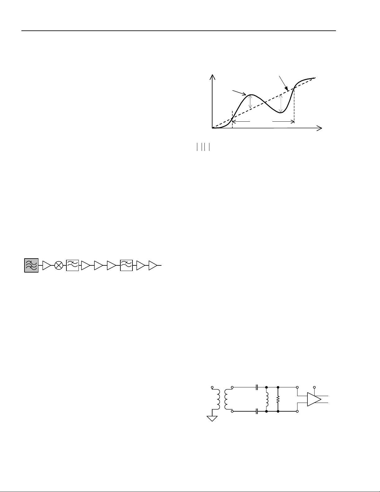
and should therefore not be used. Figure 3 is a
diagram of the gain steps.
gain accuracy is determined after calibration of the
32 dB amplifier.
ACTUAL
GAIN (dB)
ACTUAL GAIN
ACTUAL = REQUESTED
X
20 dB
Y
REQUESTED GAIN (dB)
Note: =Y,X relative gain accuracy.
Figure 4. Actual Gain vs. Requested Gain
The input impedance of the IF strip will vary slightly
when the 32 dB amplifier is switched between the ON
and OFF states. We recommend that the IF strip be
matched with the 32 dB amplifier in the ON state to
provide the best match to the SAW filter when the
input level is at a minimum. The input matching
network can match the IF input directly to the SAW
filter or to 50 Ω.
G4
32/0
*Not tested.
6
G3 G2 G6* G1G5*LPF1 LPF2
16/0
8/0
4/0
21/0
4/0
Figure 3. IF Amplifier Gain Steps
The baseband amplifier section contains dc correction
circuitry that minimizes dc offsets at the I/Q outputs.
The low-pass filters in the baseband contain a selfcalibrating circuit for tuning of filter cut-off frequency.
The selectable gain settings are programmed via the
TR register as described in the Programming
Information section. Filter tuning and dc calibration
are also explained in that section.
To achieve the specified absolute gain accuracy, the
total gain should be calibrated at room temperature.
This would normally be part of the overall phone
calibration. Absolute gain accuracy measures the gain
change over a specified temperature range relative to
the room temperature measurement. In the GSM
system, this specification is dependent on all the RX
functional blocks and not solely on the IF strip. The
relative gain accuracy is a measure of the gain stage
accuracy over a 20 dB range (see Figure 4). Relative
A matching network to 50 Ω was chosen for the
evaluation board to allow for convenient laboratory
measurements. To keep the input impedance low and
minimize impedance variation between gain settings
of the IF stage, a resistor is shunt-connected between
the input terminals. The input network can then be
matched to the desired input impedance. (The
specified gain includes a resistor value of 500 Ω.) For
testing purposes, the input has been matched to 50 Ω,
and the gains of the IF/baseband amplifier are all
referred to a 50 Ω matched input impedance. The I/Q
outputs are terminated in high-impedance loads. The
gains are voltage gains and include the voltage gain in
the impedance transformation of the input matching
network. The network is illustrated in Figure 5.
W3020 G4 bit
IFIP PIN 35
INPUT
IMPEDANCE
50
Ω
1:1
Note: Balun is shown for testing purposes only.
R1
500
Ω
IFIN PIN 34
32/0
Figure 5. IF Strip Balanced Input Matching
Network
12 Lucent Technologies Inc.

Advance Data Sheet
December 1999 W3020 GSM Multiband RF Transceiver
IF/Baseband Amplifier (continued) Table 6. IF/Baseband Amplifier Performance
VDD = 2.7 V; TA = 25 °C ± 3 °C.
Parameter Min Typ Max Unit
Total Voltage Gain (referred to 50 Ω input)*
60 65 68 dB
Demodulator Gain — 4 — dB
Absolute Gain Accuracy
Relative Gain Step Accuracy
Noise Figure (matched to 50 Ω)
†
‡
§
O/P 1 dB Compression Point (0 dB gain
–2.0 — 2.0 dB
–1.0 — 1.0 dB
— 6.2 12 dB
— –1.5 — dBm(V)**
setting)
O/P 1 dB Compression Point (>16 dB
12 — — dBm(V)**
baseband gain setting)
Output Load Capacitance (differential)
Output Load Capacitance (single-end to
— — 10 pF
— — 10 pF
ground)
Output Load Resistance (differential)
Output Load Resistance (single-end to
20 — —
40 — —
kΩ
kΩ
ground)
IF Enable Time — — — µs
I/Q Common-mode Output Voltage 0.5 * VDDB – 0.15 0.5 * VDDB 0.5 * VDDB + 0.15 V
I/Q Output Current
I/Q Phase Accuracy
I/Q Amplitude Mismatch
I/Q Differential Offset Voltage
(corrected)
§,††
Offset Correction Decay Rate
§
§
§
IF Input Impedance (diffferential)
32 dB gain setting
0 dB gain setting
* 64 dB DGC setting. This voltage gain is measured from the input of the IF strip to either the I or Q channel output.
±50
— 3.5 — degrees
–1 ±0.1 1 dB
— 5 ±50 mV
— 2 — mV/s
—
—
— — µA
114 – j497
92 – j497
—
—
Ω
Ω
† The absolute accuracy refers to the total gain variation from the nominal condition over temperature (–30 °C to +85 °C) after gain calibration at
nominal temperature.
‡ The relative gain step accuracy is determined after the 32 dB gain stage has been calibrated at nominal temperature. The total gain step accuracy
at any of the possible gain conditions should not vary more than the specified amount within a 20 dB measurement window.
§ At 64 dB gain setting.
** This is a voltage and specified in dBm as if the voltage were across a 50 Ω load.
††Offset tested in coarse dc-correction mode only.
Lucent Technologies Inc. 13

Advance Data Sheet
W3020 GSM Multiband RF Transceiver December 1999
IF/Baseband Amplifier (continued) Table 7. Low-Pass Rejection Characteristics
VDD = 2.7 V; TA = 25 °C ± 3 °C; high bandwidth.
Parameter Min Typ Max Unit
Corner Frequency* 130 168 226 kHz
Group Delay Distortion (0 kHz—75 kHz) — 61 — ns
Attenuation:
75 kHz — 0.4 — dB
100 kHz — 0.8 — dB
200 kHz — 4.7 — dB
400 kHz — 18 — dB
600 kHz — 28 — dB
800 kHz — 35 — dB
1.6 MHz — 53 — dB
3.0 MHz — 69 — dB
* After filter tuning. (See FilterTune and dc Offset Correction Tuning section.)
14 Lucent Technologies Inc.
 Loading...