

Advance Data Sheet
December 1999
W3000 PLL Dual-Band Frequency Synthesizer
Features
+ 2.2 GHz operational
+ Dual-band optimized
+ Low supply current (5.1 mA)
+ Surface-mount 14-pin TSSOP package
+ Scaled PD gain for dual-band operation
+ Programmable phase-detector polarity
+ Synchronous or forced counter update loading
+ Powerdown mode via external pin or serial bus
+ Low-load capacitance on reference input buffer
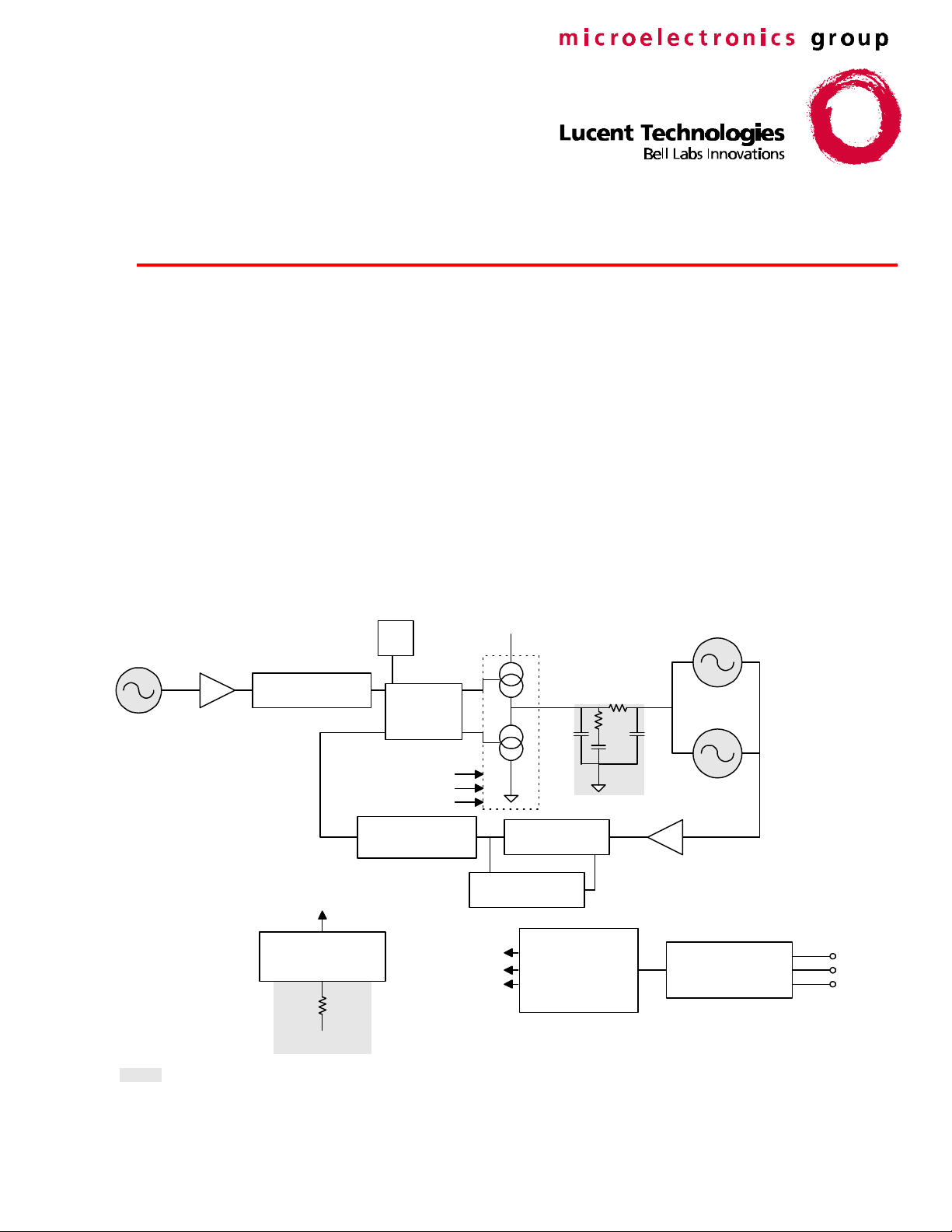
LD
REF_IN
11-BIT COUNTER
TCXO
R
PHASE
DETECTOR
Applications
+ GSM900/1800/1900
+ North American IS-136/137
+ Personal Digital Cellular (Japan RCR-27)
+ Personal Handy Phone (Japan RCR-28)
+ CDMA (IS-95)
VDDC
VCP
VCO BAND A
OFF CHIP
IREF
HIGH-PRECISION
CURRENT
REFERENCE
RREF
VDDC
IPD SETTING
PD POLARITY
11-BIT COUNTER
IREF
M
7-BIT COUNTER
IPD SETTING
PD POLARITY
BAND
PRESCALER
÷
64/65
A
CONTROL
LOGIC
Figure 1. Block Diagram with Pinout
VCO BAND B
MAIN_IN
24-BIT SERIAL
SHIFT REGISTER
LAT
DAT
CLK

Advance Data Sheet
W3000 PLL Dual-Band Frequency Synthesizer December 1999
Table of Contents
Features............................................................................................................................................................... 1
Applications .........................................................................................................................................................1
Description...........................................................................................................................................................3
Pin Information.....................................................................................................................................................4
Absolute Maximum Ratings.................................................................................................................................. 5
Electrostatic Discharge Caution............................................................................................................................ 5
Electrical Characteristics...................................................................................................................................... 6
Charge Pump Current..........................................................................................................................................7
PLL Programming Information .............................................................................................................................8
Serial Data Input..................................................................................................................................................9
Serial Bus Timing Information..............................................................................................................................9
Functional Descriptions......................................................................................................................................10
REF Register .....................................................................................................................................................11
MAIN Register....................................................................................................................................................15
PLL Lock-Detect Function..................................................................................................................................17
Typical Performance Characteristics..................................................................................................................17
MAIN_IN Input Parallel Equivalent Circuit.......................................................................................................18
Application Example ..........................................................................................................................................18
Application Information ...................................................................................................................................... 19
Typical Performance Data..................................................................................................................................22
Outline Diagram................................................................................................................................................. 26
14-Pin TSSOP ................................................................................................................................................26
Manufacturing Information ................................................................................................................................. 27
Ordering Information..........................................................................................................................................27
Lucent Technologies Inc.2
Advance Data Sheet
December 1999 W3000 PLL Dual-Band Frequency Synthesizer
Description
The W3000 is a high-performance UHF RF PLL synthesizer, designed for use in digital wireless communication
applications. Particular emphasis in the design has been placed on dual-band applications, with near-seamless
switching between operational bands without the need for external loop-filter circuitry other than that required for
single band applications. In combination with a suitable reference crystal, UHF VCO, and associated loop-filter
components, the W3000 offers a very low-noise oscillator solution.
The reference signal is divided by a programmable 11-bit counter to provide a wide range of comparison
frequencies, allowing compliance with the various standards. The reference input is rising-edge triggered, and we
recommend that an inverting buffer be used when the W3000 is interfaced to a commercial TCXO.
The MAIN_IN signal normally associated with the UHF VCO is fed into a dual modulus prescaler (64/65) and is
then divided by the 11-bit main counter to be compared to the output of the reference counter in a digital phase
detector.
The W3000 is implemented with programmable charge-pump currents to allow fast switching between bands for
dual-band applications, without changing the loop filter. The charge pump can be programmed internally, or
externally with a resistor (recommended). Charge pump outputs can be disabled, thereby allowing open-loop
VCO modulation schemes.
With synchronous reloading, the counter reloads a new programmed value when the counter reaches zero. With
forced counter reloading, the reloading occurs when the programmed word is latched in. These techniques can
improve lock time when performing a dual-band hop or in start-up conditions.
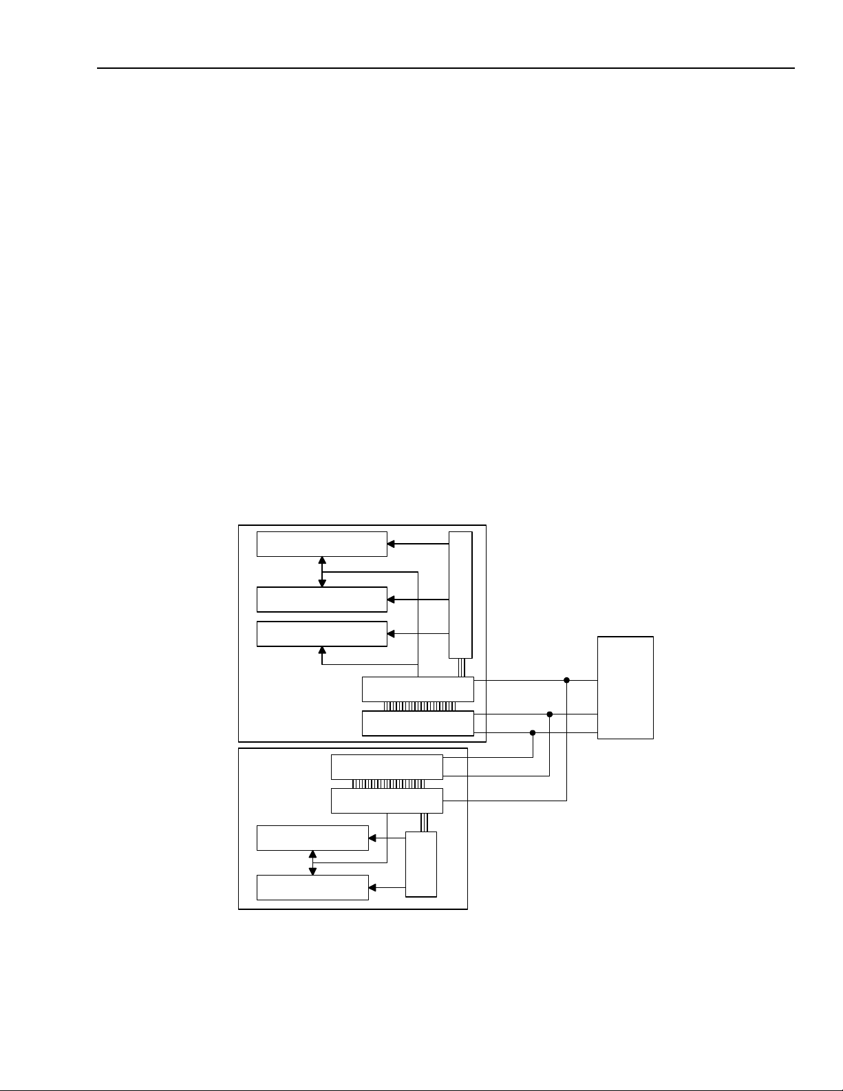
The W3000 uses a standard 3-wire programming bus (data, enable, clock) that operates up to 10 MHz. This
serial interface is via a 24-bit word that incorporates both register addressing and device addressing allowing two
chips to share the bus.
TR REGISTER
CONFIG REGISTER
MAIN REGISTER
W3020
W3000
MAIN REGISTER
A[0:2]
PARALLEL LATCH
SERIAL SHIFT
SERIAL SHIFT
PARALLEL LATCH
ADDRESS DECODER
LAT
CLK
DAT
DAT
CLK
LAT
A[0:2]
SC1
SERLE1
SERCK
SERDA
REF REGISTER
ADDRESS
DECODER
Figure 2. Serial Bus Programming
Lucent Technologies Inc. 3
Advance Data Sheet
W3000 PLL Dual-Band Frequency Synthesizer December 1999
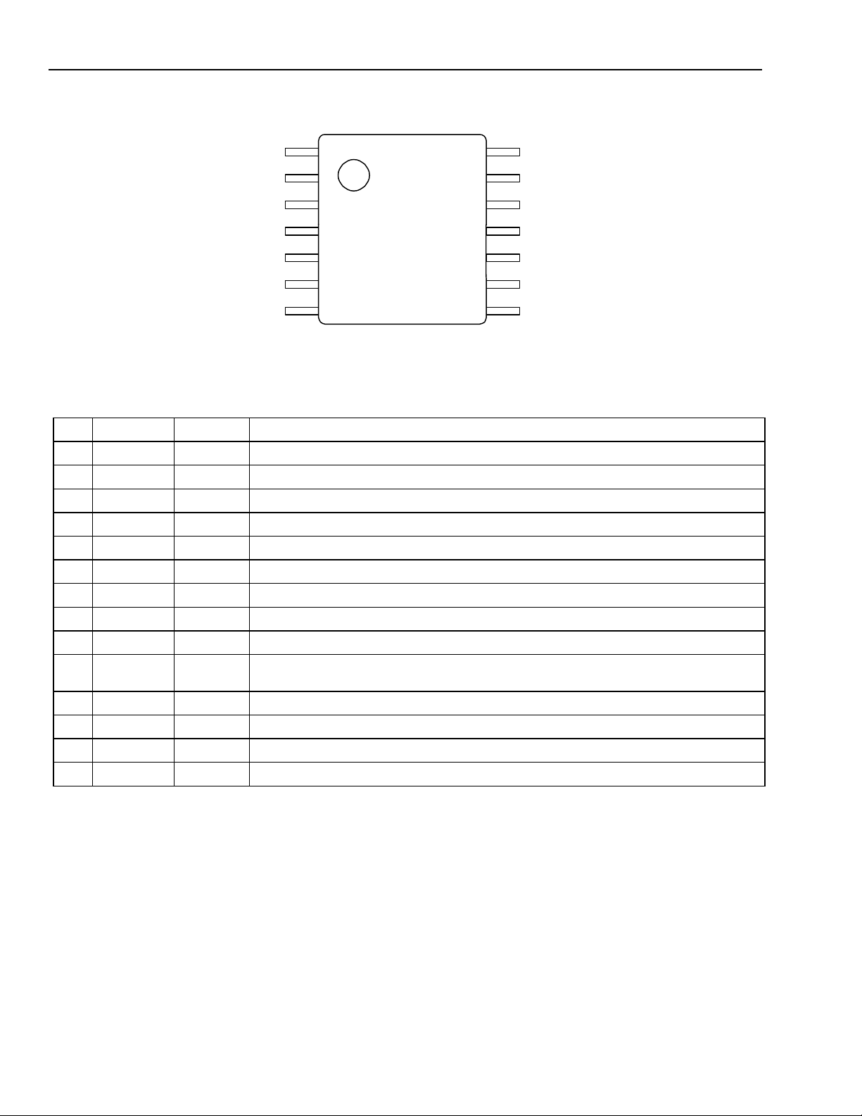
Pin Information
VDDC
CPOUT
VSS1
VSS2
MAIN_IN
VDD1
VDD2
1
2
3
4
5
6
7
14
13
12
11
10
9
8
LAT
DAT
CLK
PWRDN
REF_IN
RES
LOCKDET
Figure 3. Pin Diagram
Table 1. Pin Descriptions
Pin Symbol Function Name/Description
1 VDDC Supply
2 CPOUT Output
3 VSS1 Ground
4 VSS2 Ground
5 MAIN_IN Input
6 VDD1 Supply
7 VDD2 Supply
8 LOCKDET Output
9 RES Input
10 REF_IN Input
Charge Pump Positive Supply Voltage. Must be ≥VDD. (VDD = VDD1 = VDD2).
Charge Pump Output.
Ground 1. Charge pump and logic ground.
Ground 2. Prescaler and reference ground.
VCO Signal Input. Must be ac-coupled.
Voltage Supply 1. Prescaler supply voltage.
Voltage Supply 2. Logic and reference supply (must be equal to VDD1).
Lock Detect Output.
External Resistor Input. Add resistor to VDDC if required (>10 kΩ).
Reference Frequency Input. Connection from reference oscillator. Must be ac-
coupled.
11 PWRDN Input
12 CLK Input
13 DAT Input
14 LAT Input
Powerdown. For low current operation. (Low is powerdown mode.)
Serial Input. Programming clock line.
Serial Input. Programming data line.
Serial Input. Programming latch line.
Lucent Technologies Inc.4
Advance Data Sheet
December 1999 W3000 PLL Dual-Band Frequency Synthesizer
Absolute Maximum Ratings
Stresses in excess of the absolute maximum ratings can cause permanent damage to the device. These are
absolute stress ratings only. Functional operation of the device is not implied at these or any other conditions in
excess of those given in the operations sections of the data sheet. Exposure to absolute maximum ratings for
extended periods can adversely affect device reliability.
Parameter Symbol Min Max Unit
Ambient Operating Temperature TA –30 85 °C
Storage Temperature Tstg –65 150 °C
Lead Temperature (soldering, 10 s) TL — 300 °C
Positive Supply Voltage VDD 0 4.5 Vdc
Positive Charge Pump Supply Voltage VDDC 0 4.5 Vdc
Power Dissipation PD — 250 mW
ac Input Voltage — 0 VDD Vp-p
Digital Voltages — Vss – 0.3 VDD + 0.3 Vdc
Electrostatic Discharge Caution
Although protection circuitry has been designed into this device, proper precautions should be taken to avoid
exposure to electrostatic discharge (ESD) during handling and mounting. Lucent Technologies Microelectronics
Group employs a human-body model (HBM) and a charged-device model (CDM) for ESD-susceptibility testing
and protection design evaluation. ESD voltage thresholds are dependent on the circuit parameters used to define
the model. No industry-wide standard has been adopted for CDM. However, a standard HBM (resistance =
1500 Ω, capacitance = 100 pF) is widely used and, therefore, can be used for comparison purposes.
Parameter Model Min Max Unit
ESD Threshold Voltage HBM 1000 — V
ESD Threshold Voltage (corner pins) CDM 1000 — V
ESD Threshold Voltage (noncorner pins) CDM 1500 — V
Lucent Technologies Inc. 5
Advance Data Sheet
W3000 PLL Dual-Band Frequency Synthesizer December 1999
Electrical Characteristics
Table 2. General Specifications
Conditions (unless otherwise specified): VDD = 2.7 V; TA = 25 °C ± 3 °C; VREF = 0.25 Vp-p, VDDC = 2.85 V.
Parameters Symbol Min Typ Max Unit
Ambient Operating Temperature TA –30 25 85
Nominal Operating Voltage VDD 2.7 2.85 3.6 V
Nominal Charge Pump Operating Voltage VDDC VDD 2.85 3.6 V
Power Supply Current
Powerdown Current
‡
†
IDD — 5.1 8.0 mA
IDD — 0.1 20
Digital Inputs:
Logic High Voltage VIH 0.7 * VDD VDD VDD + 0.15 V
Logic Low Voltage VIL – 0.3 GND 0.3 * VDD V
Logic High Current (VIH = VDD + 0.15 V) |IIH| — — 10
Logic Low Current (VIL = –0.3 V) |IIL| — — 10
Digital Outputs:
Logic High Voltage (|IOH| = 2 mA) VOH VDD – 0.4 — — V
Logic Low Voltage (|IOL| = 2 mA) VOL — — 0.4 V
† (IDD1 + IDD2 + IDDC) under locked condition, VDDC = 2.85 V; fVCO.= 1200 MHz; fREF = 13 MHz.
‡ (IDD1 + IDD2 + IDDC) VIL = 0 Vdc on all logic input pins.
°C
µA
µA
µA
Table 3. Electrical Specifications
Conditions (unless otherwise specified): VDD = 2.7 V; TA = 25 °C ± 3 °C; VREF = 0.25 Vp-p, VDDC = 2.85 V.
Parameter Symbol Min Typ Max Unit
Main Input Frequency Range fVCO 0.5 — 2.2 GHz
Main Input Level (1100 MHz—1750 MHz) VMAIN –20 — 6
Main Input Level
†
VMAIN –10 — 6
dBm/50 Ω*
dBm/50 Ω*
Reference Input Frequency Range fREF 8 — 30 MHz
Reference Input Shunt Resistance — 20 30 —
kΩ
Reference Input Shunt Capacitance — — 1.2 3 pF
Reference Input Slew Rate — 41 60 — mV/ns
Reference Input Level VREF 0.25 — 2.00 Vp-p
Phase Detector Comparison Frequency fCOMP 0.025 — 2 MHz
External Resistor Value (pin 9 to VDDC) — 10 18 —
Phase Detector Range —
Phase Detector Noise Floor, ±150 Hz
offset (25 kHz comparison frequency)
*Equivalent voltage of a 50 Ω terminated source.
† Frequencies outside the 1100 MHz—1750 MHz range and up to and including 2200 MHz.
‡ fVCO = 1190 MHz; VREF = 1.4 Vp-p.
‡
— — –167 — dBc/Hz
–2 π
—
2 π
kΩ
rad.
Lucent Technologies Inc.6
Advance Data Sheet
December 1999 W3000 PLL Dual-Band Frequency Synthesizer
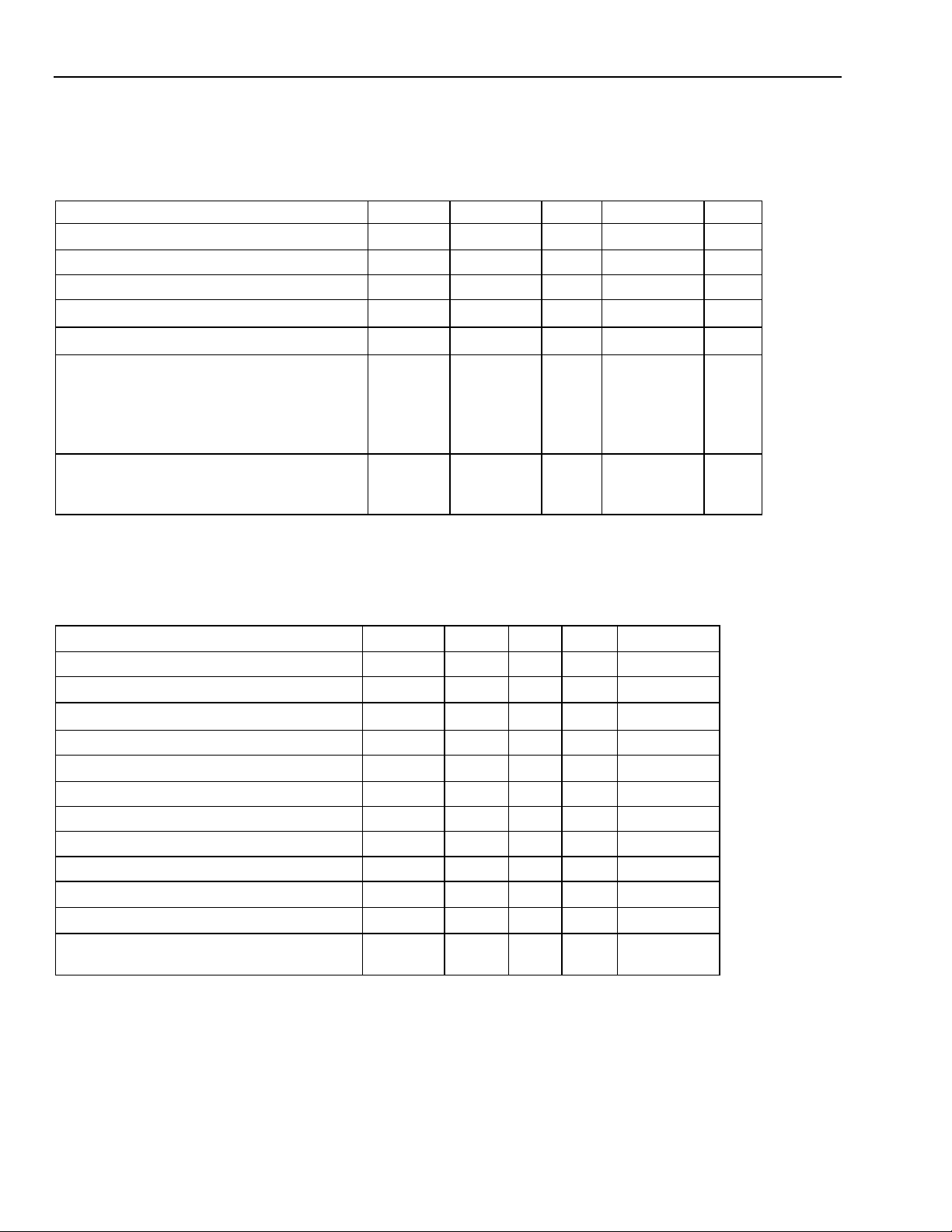
Charge Pump Current
ICP-DN (T = 25 °C )
A
B
C
D
E
F
ICP/mA
COMPLIANCE
RANGE
0.4 V
ICP-UP (T = 25 °C )
COMPLIANCE
RANGE
VDDC – 0.4 V
0.4 2.45
A: CP UP CURRENT AT VCP = VDDC – 0.4.
B: CP UP CURRENT AT VCP = VDDC/2.
C: CP UP CURRENT AT VCP = 0.4.
VDDC/2
VCP
D: CP DOWN CURRENT AT VCP = 0.4 V.
E: CP DOWN CURRENT AT VCP = VDDC/2.
F: CP DOWN CURRENT AT VCP = VDDC – 0.4.
Figure 4. Charge Pump Current vs. Voltage
Table 4. Charge Pump Specifications
Conditions (unless otherwise specified): VDD = 2.7 V; TA = 25 °C ± 3 °C; VDDC = 2.85 V; VCP = VDDC/2;
RREF = 18 kΩ.
Parameter
Charge Pump Output Current
Conditions Symbol Min Typ Max Unit
ICP = 0.7 mA IUP 0.6 0.7 0.8 mA
ICP= 0.7 mA IDN –0.8 –0.7 –0.6 mA
ICP = 0.9 mA IUP 0.8 0.9 1.0 mA
ICP = 0.9 mA IDN –1.0 –0.9 –0.8 mA
ICP = 1.9 mA IUP 1.6 1.9 2.2 mA
ICP = 1.9 mA IDN –2.2 –1.9 –1.6 mA
ICP = 2.5 mA IUP 2.1 2.5 2.9 mA
ICP = 2.5 mA IDN –2.9 –2.5 –2.1 mA
CP High-Impedance State
Current
CP Sink vs. Source Mismatch
CP Current vs. Voltage
2
0.4 < VCP < VDDC – 0.4 V,
–30 °C < TA < +85 °C
1
TA = 25 °C — — 3 15 %
0.4 < VCP < VDDC – 0.4 V,
ITRI — 0.1 20 nA
— — 2 8.5 %
TA = 25 °C
CP Current vs Temperature
Notes (refer to Figure 4 for definitions):
1. ICP-DN vs ICP-UP = charge pump output current up vs down mismatch = [|E| – |B|]/[ 1/2 * {|E| + |B|}] * 100%.
2. ICP vs VCP = charge pump output current magnitude variation vs voltage = [ 1/2 * {|F| – |D|}]/[1/2 * {|F| +|D|}] * 100% and
[1/2 * {|A| - |C|}]/[1/2 *{|A| + |C|}] * 100%.
3. ICP vs TA = charge pump output current magnitude variation vs. temperature = [|E @ temp| – |E @ 25 °C|]/|E @ 25 °C| * 100% and [|B @
temp| – |B @ 25 °C|]/|B @ 25°C| * 100%.
3
–30 °C < TA < +85 °C — — 8 10 %
Lucent Technologies Inc. 7

Advance Data Sheet
[
]
f
M
A
f
R
[
]
[
]
W3000 PLL Dual-Band Frequency Synthesizer December 1999
PLL Programming Information
The oscillator frequency is selected according to the following expression:
f*A)M* P(
REF
f
VCO
=
where:
VCO = VCO frequency
P/(P + 1) = Dual modulus prescaler
= Programmable counter ratio (2 to 2047), M > A
= Swallow counter ratio (0 to M – 1 or 127)
REF = External reference oscillator frequency
= Reference counter ratio (2 to 2047)
Example
You wish to have a VCO operating at 1172 MHz, ability to step the frequency in 200 kHz steps, and a reference
clock at 13 MHz.
+
R
Step 1:
Calculate the reference counter ratio R
64
MHz 13
=
91
=
R ==
Step 2: Calculate M & A
f
VCO
1172+=
5860
M is an integer, and so is A; therefore, M = 91, and A = 36.
65
kHz 200
f* A)M* P(
REF
+
R
13* A)M* 64(
65
65*1172
)AM*64( ==+
36
64
13
5860
Lucent Technologies Inc.8
Advance Data Sheet
LSB
tLLt
CWHtCWL
December 1999 W3000 PLL Dual-Band Frequency Synthesizer
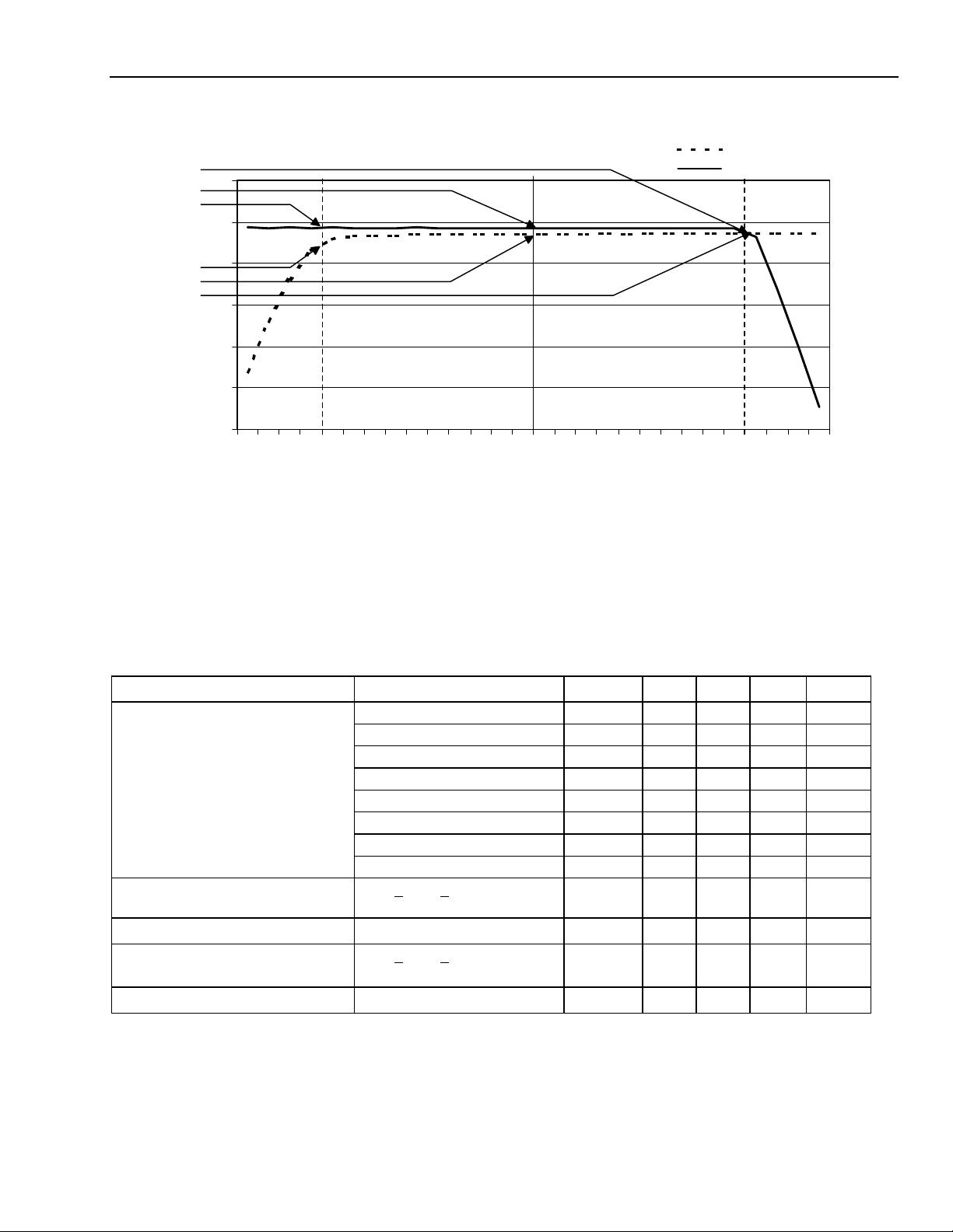
Serial Data Input
The PLL is programmed via a 3-wire serial bus, utilizing a data pin (DAT), a clock pin (CLK), and a latch pin
(LAT).
Serial Bus Timing Information
DAT
MSB
CLK
LAT
CS
t
MSB – 1
CH
t
LS
t
OR
LAT
V
LWH
t
Figure 5. Serial Bus Timing Diagram
Table 5. Serial Bus Timing Information
Symbol Parameter Min Typ Max Unit
tCS Data to Clock Setup Time 33 — — ns
tCH Data to Clock Hold Time 10 — — ns
tCWH Clock Pulse Width High 33 — — ns
tCWL Clock Pulse Width Low 33 — — ns
tLS Clock Falling Edge to Latch High Setup Time 0 — — ns
tLWH Latch Pulse Width 50 — — ns
tLL Latch to Clock Setup Time 33 — — ns
fCLK Clock Input Frequency — — 10 MHz
Lucent Technologies Inc. 9
 Loading...