

AGERE LUCL8575BR Datasheet

Advance Data Sheet
March 1997
L8575 Dual-Resistive, Low-Cost
Subscriber Line Interface Circuit (SLIC)
Features
■
Two channels in a single package
■
Serial data interface
■
Per-channel powerdown
■
Low standby power ( ≤ 65 mW per channel)
■
Integrated protection
■
No external protection device required
■
Battery noise cancellation
■
Switchhook detector
■
Ring-trip detector
■
Switchhook and ring-trip detector self-test
■
Fault detector
■
Zero ring voltage cross detection
■
Three relay drivers per channel
■
44-pin, surface-mount, plastic package (PLCC)
Description
The L8575 is a dual-resistive, low-cost subscriber
line interface circuit (SLIC) that is optimized to meet
both ITU-T recommendations and LSSGR requirements for 600 Ω /900 Ω resistive and complex impedance termination applications. It interfaces the lowvoltage circuits on an analog line card to the Tip and
Ring of two subscriber loops. The L8575 does not
supply dc current to the subscriber loops—external
resistors are used for this purpose. The de vice is built
using a 90 V complementary bipolar (CBIC) process
and is available in a 44-pin PLCC package.

L8575 Advance Data Sheet
Dual-Resistive, Low-Cost SLIC March 1997
2 Lucent Technologies Inc.
Table of Contents
Contents Page
Features .................................................................................................................................................................. 1
Description ...............................................................................................................................................................1
Preliminary Pin Information ..................................................................................................................................... 5
Absolute Maximum Ratings (@ T
A
= 25 ° C)............................................................................................................ 8
Electrical Characteristics......................................................................................................................................... 9
Relay Drivers..................................................................................................................................................... 11
Transmission...................................................................................................................................................... 13
Serial Interface and Logic.................................................................................................................................. 14
Applications........................................................................................................................................................... 16
General.............................................................................................................................................................. 16
Resistor Module................................................................................................................................................. 16
Protection .......................................................................................................................................................... 18
Tip/Ring Drivers................................................................................................................................................. 20
Receive Interface............................................................................................................................................... 20
Transmit Interface.............................................................................................................................................. 20
Battery Noise Cancellation................................................................................................................................ 20
On-Hook Transmission....................................................................................................................................... 21
Self-Test............................................................................................................................................................. 21
Serial Data Interface.......................................................................................................................................... 21
Operating States.................................................................................................................................................... 24
Active State........................................................................................................................................................ 24
Test State........................................................................................................................................................... 24
Powerdown State with Relay Driver RDD Operated.......................................................................................... 24
Powerdown State............................................................................................................................................... 24
Ringing State (D2 = 1)....................................................................................................................................... 24
Supervision............................................................................................................................................................ 25
Off-Hook Detection............................................................................................................................................ 25
Ring-Trip Threshold ........................................................................................................................................... 25
Ring-Trip Requirements......................................................................................................................................25
Fault Detection................................................................................................................................................... 26
Zero Voltage Current Cross............................................................................................................................... 26
Relay Drivers..................................................................................................................................................... 26
dc Characteristics.................................................................................................................................................. 27
I/V Characteristics ............................................................................................................................................. 27
Loop Length....................................................................................................................................................... 27
ac Design............................................................................................................................................................... 28
Codec Features and Selection Summary.......................................................................................................... 28
Design Equations .............................................................................................................................................. 29
Application Diagram ..............................................................................................................................................33
Outline Diagram..................................................................................................................................................... 35
44-Pin PLCC...................................................................................................................................................... 35
Ordering Information ..............................................................................................................................................36

Lucent Technologies Inc. 3
Advance Data Sheet L8575
March 1997 Dual-Resistive, Low-Cost SLIC
Table of Contents
(continued)
Tables Page
Table 1. Pin Descriptions.......................................................................................................................................... 5
Table 2. Operating Conditions and Powering ............................................................................................................9
Table 3. Battery Feed, Switchhook Detectors (LCA and LCB), and Fault Detectors (FLTA and FLTB)................... 10
Table 4. Ring-Trip Detectors (RTA, RTB, RZA, and RZB)....................................................................................... 10
Table 5. Relay Drivers (RDRA, RDTA, RDRB, RDTB, RDDA, and RDDB)............................................................. 11
Table 6. Analog Signal Pins.................................................................................................................................... 11
Table 7. Transmission Characteristics..................................................................................................................... 13
Table 8. Logic Inputs (CLK, EN, and DI) and Outputs (DO).................................................................................... 14
Table 9. Timing Requirements for CLK, EN, DI, and DO........................................................................................ 14
Table 10.
MMC
* A31A8575AA Thick Film Resistor Module.................................................................................... 17
Table 11. Total Module Power Dissipation .............................................................................................................. 19
Table 12. Truth Table for EN and CLK..................................................................................................................... 22
Table 13. Output DATA Bit Definition .......................................................................................................................22
Table 14. Input DATA Bit Definition.......................................................................................................................... 23
Table 15. Truth Table for D1 and D0........................................................................................................................ 24
Table 16. External Components Required...............................................................................................................33
Figures Page
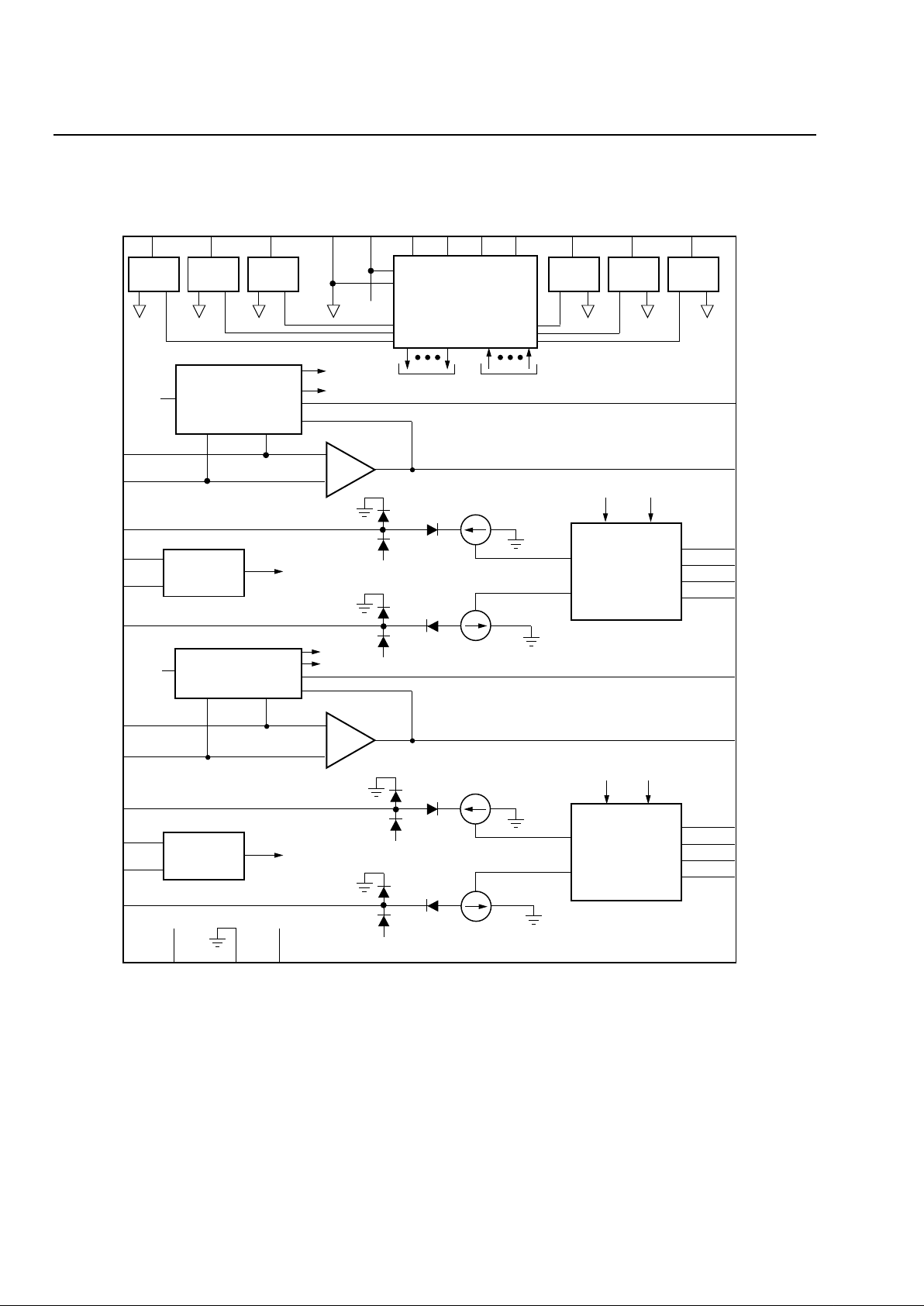
Figure 1. Functional Diagram ....................................................................................................................................4
Figure 2. 44-Pin PLCC Pinout.................................................................................................................................. 5
Figure 3. Power Supply Rejection vs. Frequency Diagram..................................................................................... 15
Figure 4. L8575 SLIC Resistor Module................................................................................................................... 17
Figure 5. L8575 SLIC Dual-Resistive Matching Requirements .............................................................................. 18
Figure 6. Self-Test Mode Circuit ............................................................................................................................. 21
Figure 7. Timing Requirements for CLK, EN, DI, and DO ...................................................................................... 22
Figure 8. Logic Diagram (Positive Logic; Flip-Flops Clocked on High-to-Low Transition)....................................... 23
Figure 9. Ring-Trip Threshold................................................................................................................................. 25
Figure 10. Ring-Trip Circuits ...................................................................................................................................25
Figure 11. L8575 SLIC I/V Template .......................................................................................................................27
Figure 12. Equivalent Complex Terminations ..........................................................................................................29
Figure 13. Initial ac Interface for Complex Termination Between L8575 SLIC and T7504 Codec ..........................30
Figure 14. Revised ac Interface C
T
and C
R
Combined into a Single Capacitor C
S
..................................................31
Figure 15. Addition of Resistor R
SC
from XMT to IRP .............................................................................................32
Figure 16. Typical Application Diagram with Blocking Capacitors (C
B
) Included ....................................................34
*
MMC
is a registered trademark of Microelectronic Modules Corporation.
L8575 Advance Data Sheet
Dual-Resistive, Low-Cost SLIC March 1997
4 Lucent Technologies Inc.
Description
(continued)
12-3304(F).ar1
Figure 1. Functional Diagram
RELAY
DRIVER
RELAY
DRIVER
SERIAL DATA INTERFACE,
LATCHES, AND LOGIC
RELAY
DRIVER
RELAY
DRIVER
AXA
RING-TRIP
DETECTOR A
RECEIVE
INTERFACE AND
BATTERY NOISE
CANCELLATION A
–
+
CONTROL DETECTORS
VBAT
SWITCHHOOK
AND
FAULT DETECTORS A
VBAT
TIP CURRENT
SOURCE A
RING CURRENT
SOURCE A
AXB
–
+
VBAT
SWITCHHOOK
AND
FAULT DETECTORS B
RING-TRIP
DETECTOR B
RECEIVE
INTERFACE AND
BATTERY NOISE
CANCELLATION B
VBAT
TIP CURRENT
SOURCE B
RING CURRENT
SOURCE B
RDDA RDRA DGND V
DDD DI DO CLK EN RDTB RDRB
TSA
RSA
PTA
RTPA
RTNA
PRA
TSB
RSB
PTB
RTPB
RTNB
PRB
RGBNB
CBNB
IRPB
VRNB
XMTB
CFLTB
RGBNA
CBNA
IRPA
VRNA
V
DDA AGND VBAT
XMTA
CFLTA
NRTB
VBAT
TSTB PDB
VBAT
TSTA PDA
NRTA
NLCA
NFLTA
RELAY
DRIVER
RDRA
+5D
RELAY
DRIVER
RDDB
+5 A
V
BAT
NPLTB
NLCB
Lucent Technologies Inc. 5
Advance Data Sheet L8575
March 1997 Dual-Resistive, Low-Cost SLIC
Preliminary Pin Information
12-3364(F)
Figure 2. 44-Pin PLCC Pinout
Table 1. Pin Descriptions
Pin Symbol Type Name/Function
1
NC —
No Connect. Unused pin (no internal connection).
2 DO O
Serial Data Output. Data in the internal 8-bit serial shift register is shifted out on this logic
output with the clock signal on pin CLK.
3 DI I
Serial Data Input. Data on this logic input is shifted into the 8-bit serial shift register with
the clock signal on pin CLK.
4 CFLTB I/O
Fault Filter (Channel B). Connect a 0.1 µ F capacitor from CFLTB to AGND. This capaci-
tor filters Tip/Ring transients from the channel B fault detector.
5 V
DDD
—
5 V Digital dc Supply. 5 V supply for logic and relay driver flyback diodes.
6 DGND —
Digital Ground. Ground for channel B relay drivers.
7 RDDB O
Disconnect Relay Driver (Channel B). This output drives the external relay.
8 RDRB O
Ringing Relay Driver (Channel B). This output drives an external ringing relay.
9 RDTB O
Test Relay Driver (Channel B). This output drives an external test relay.
10 RTPB I
Ring-Trip Positive (Channel B). Positive sense input for the ring-trip detector.
RDRA
RTPA
RDTA
XMTA
TSA
RSA
RGBNA
VRNA
RTPB
RDTB
RDRB
XMTB
TSB
RSB
RGBNB
VRNB
7
9
10
11
12
13
14
15
16
17
8
6 4 3 2 1 44434241405
18 20 21 22 23 24 25 26 27 2819
39
37
36
35
34
33
32
31
30
29
38
RDDB
RTNB
RTNA
PTA
PRA
AGND
CBNA
CBNB
AGND
PTB
PRB
V
DDD
DI
NC
CFLTB
CLKDOEN
DGND
CFLTA
V
DDD
DGND
RDDA
IRPA
VBAT
VDDA
VBAT
IRPB
L8575

L8575 Advance Data Sheet
Dual-Resistive, Low-Cost SLIC March 1997
6 Lucent Technologies Inc.
Preliminary Pin Information
(continued)
Table 1. Pin Descriptions (continued)
Pin
Symbol Type Name/Function
11
RTNB I
Ring-Trip Negative (Channel B). Negative sense input for the ring-trip detector.
12 XMTB O
Transmit Signal Output (Channel B). Channel B transmit amplifier output.
13 TSB I
Tip Sense (Channel B). Negative input of channel B transmit op amp. Connect one high-
value resistor between TSB and the Tip of loop B and another high-value resistor between
TSB and XMTB.
14 RSB I
Ring Sense (Channel B). Positive input of channel B transmit op amp. Connect one high-
value resistor between RSB and the Ring of loop B and another high-value resistor between
RSB and AGND.
15 RGBNB I
Battery Noise Gain Resistor (Channel B). The current flowing out of PRB is 50 times the
current flowing into RGBNB. Connect a resistor from RGBNB to A GND to set the gain of the
channel B battery noise cancellation circuit.
16 VRNB I
Receive Voltage Negative Input (Channel B). The differential current flowing from PTB to
PRB is –200 times the voltage applied to VRNB, divided by the impedance connected
between IRPB and AGND.
17 IRPB I
Receive Current Positive Input (Channel B). The differential current flowing from PTB to
PRB is 200 times the current flowing into IRPB.
18 PTB O
Protected Tip (Channel B). Output of the Tip current drive amplifier B. Connect PTB to the
Tip of loop B through an overvoltage protection resistor (1.4 k Ω minimum).
19 PRB O
Protected Ring (Channel B). Output of the Ring current drive amplifier B. Connect PRB to
the Ring of loop B through an overvoltage protection resistor (1.4 k Ω minimum).
20 AGND —
Analog Signal Ground. Signal ground for channel B.
21 V
BAT
—
Office Battery Supply. Negative office battery supply for channel B.
22 CBNB I
Battery Noise Capacitor (Channel B). The current flowing out of PRB is –50 times the
voltage applied to CBNB, divided by the impedance connected between RGBNB and
AGND. Couple V
BAT
to CBNB through a high-pass filter to eliminate battery noise from the
Tip/Ring of channel B.
23 V
DDA
—
5 V Analog dc Supply.
24
CBNA I
Battery Noise Capacitor (Channel A). The current flowing out of PRA is –50 times the
voltage applied to CBNA, divided by the impedance connected between RGBNA and
AGND. Couple V
BAT
to CBNA through a high-pass filter to eliminate battery noise from the
Tip/Ring of channel A.
25 V
BAT
—
Office Battery Supply. Negative office battery supply for channel A.
26 AGND —
Analog Signal Ground. Signal ground for channel A.
27 PRA O
Protected Ring (Channel A). Output of the Ring current drive amplifier A. Connect PRA to
the Ring of loop A through an overvoltage protection resistor (1.4 k Ω minimum).
28 PTA O
Protected Tip (Channel A). Output of the Tip current drive amplifier A. Connect PTA to the
Tip of loop A through an overvoltage protection resistor (1.4 k Ω minimum).
29 IRPA I
Receive Current Positive Input (Channel A). The differential current flowing from PTA to
PRA is 200 times the current flowing into IRPA.
30 VRNA I
Receive Voltage Negative Input (Channel A). The differential current flowing from PTA to
PRA is –200 times the voltage applied to VRNA, divided by the impedance connected
between IRPA and AGND.

Lucent Technologies Inc. 7
Advance Data Sheet L8575
March 1997 Dual-Resistive, Low-Cost SLIC
Preliminary Pin Information
(continued)
Table 1. Pin Descriptions (continued)
Pin
Symbol Type Name/Function
31
RGBNA I
Battery Noise Gain Resistor (Channel A). The current flowing out of PRA is 50 times
the current flowing into RGBNA. Connect a resistor from RGBNA to AGND to set the
gain of the channel A battery noise cancellation circuit.
32 RSA I
Ring Sense (Channel A). Positive input of channel A transmit op amp. Connect one
high-value resistor between RSA and the Ring of loop A and another high-value resistor between RSA and AGND.
33 TSA I
Tip Sense (Channel A). Negative input of channel A transmit op amp. Connect one
high-value resistor between TSA and the Tip of loop A and another high-value resistor
between TSA and XMTA.
34 XMTA O
Transmit Signal Output (Channel A). Channel A transmit amplifier output.
35 RTNA I
Ring-Trip Negative (Channel A). Negative sense input for the ring-trip detector.
36 RTP A I
Ring-Trip Positive (Channel A). Positive sense input for the ring-trip detector.
37 RDTA O
Test Relay Driver (Channel A). This output drives an external test relay.
38 RDRA O
Ringing Relay Driver (Channel A). This output drives the external ringing relay.
39 RDDA O
Disconnect Relay Driver (Channel A). This output drives an external relay.
40 DGND —
Digital Ground. Ground for channel A relay drivers.
41 V
DDD
—
5 V Digital dc Supply. 5 V supply for logic and relay driver flyback diodes.
42 CFLTA I/O
Fault Filter (Channel A). Connect a 0.1 µF capacitor from CFLTA to AGND. This
capacitor filters Tip/Ring transients from the channel A fault detector.
43 EN I Enable. A high-to-low transition on this logic input latches the data in the 8-bit serial
shift register into the output latches. The logic level of EN also controls which data is
shifted into the 8-bit serial shift register (refer to CLK pin description).
44 CLK I Clock. When the enable input (EN) is high, a low-to-high transition on this logic input
shifts data at the data input pin (DI) into the 8-bit serial shift register. When the enable
input (EN) is low , a low-to-high tr ansition latches the states of the internal detectors into
the 8-bit serial shift register.

L8575 Advance Data Sheet
Dual-Resistive, Low-Cost SLIC March 1997
8 Lucent Technologies Inc.
Absolute Maximum Ratings (@ T A = 25 °C)
Stresses in excess of the absolute maximum ratings can cause permanent damage to the device. These are absolute stress ratings only. Functional operation of the device is not implied at these or any other conditions in excess
of those given in the operational sections of this data sheet. Exposure to absolute maximum ratings for extended
periods can adversely affect device reliability.
Notes:
Analog and battery voltages are referenced to AGND; digital (logic) voltages are referenced to DGND.
The IC can be damaged unless all ground connections are applied before, and removed after, all other connections. Furthermore, when powering the device, the user must guarantee that no external potential creates a voltage on any pin of the device that exceeds the device ratings.
Some of the known examples of conditions that cause such potentials during powering are (1) an inductor connected to Tip and Ring that can
force an overvoltage on VBAT through external components if the VBAT connection chatters, and (2) inductance in the VBAT lead that could reso-
nate with the VBAT filter capacitor to cause a destructive overvoltage.
Parameter Symbol Min Value Max Unit
5 V Analog dc Supply VDDA –0.5 — +7.0 V
5 V Digital dc Supply VDDD –0.5 — +7.0 V
Office Battery Supply VBAT –65 — +0.5 V
Logic Input Voltage — –0.5 — VDDD + 0.5 V
Logic Input Clamp Diode Current, per Pin — — ±20 — mA
Logic Output Voltage — –0.5 — VDDD + 0.5 V
Logic Output Current, per Pin (excluding relay drivers) — — ±35 — mA
Maximum Junction Temperature — — 150 — °C
Operating Temperature Range — –40 — +125 °C
Storage Temperature Range Tstg –40 — +125 °C
Relative Humidity Range — 5 — 95 %
Ground Potential Difference (DGND to AGND) — +0.5 — –0.5 V

Advance Data Sheet L8575
March 1997 Dual-Resistive, Low-Cost SLIC
Lucent Technologies Inc. 9
Electrical Characteristics
Generally, minimum and maximum values are testing requirements. Ho wever, some parameters may not be tested
in production because they are guaranteed by design and de vice characterization. Typical values reflect the design
center or nominal value of the parameter; they are for information only and are not a requirement. Minimum and
maximum values apply across the entire temperature range (–40 °C to +85 °C) and entire battery range (–42 V to
–58 V). Unless otherwise specified, typical values are defined as 25 °C, VDDA = 5 V, VDDD = 5 V, VBAT = –48 V. Posi-
tive currents flow into the device.
Table 2. Operating Conditions and Powering
1.Not to exceed 26 grams of water per kilogram of dry air.
2.Includes VBAT current through the external dc feed resistors, assuming the loop is open.
3.Includes power dissipation in the external dc feed resistors per application diagram, assuming the loop is open.
4.VBAT power supply rejection depends on the battery noise cancellation circuit. The performance stated here applies only during the active
state and assumes proper battery noise cancellation, i.e., a high-pass filter from VBAT to CBN and a resistor from RGBN to AGND which is 50
times the dc feed resistor connecting VBAT to Ring (refer to the application diagram).
5.This parameter is not tested in production. It is guaranteed by design and device characterization.
Parameter Min Typ Max Unit
Temperature Range –40 — 85 °C
Humidity Range 5 —
95
1
%RH
Supply Voltage:
VDDA
VDDD
VBAT
VDDA – VDDD
4.75
4.75
–42
—
—
—
–48
—
5.5
5.5
–58
±0.5
V
V
V
V
Supply Currents (both channels active):
IVDDA + IVDDD (5 V)
I
VBAT (–48 V)
2
—
—
—
—
19.0
–27.5
mA
mA
Supply Currents (both channels powerdown):
IVDDA + IVDDD (5 V)
IVBAT (–48 V)
2
—
—
—
—
18.0
–2.0
mA
mA
Total Power Dissipation (5 V; –48 V)3:
Active (both channels)
Powerdown (both channels)
—
—
—
—
1.40
185
W
mW
Power-supply Rejection
4, 5
(50 mVrms ripple):
Tip/Ring and XMT
Refer to Figure 3.
Thermal5:
Thermal Resistance (still air)
Operating Tjc
—
—
—
—
47
155
°C/W
°C

L8575 Advance Data Sheet
Dual-Resistive, Low-Cost SLIC March 1997
10 Lucent Technologies Inc.
Electrical Characteristics (continued)
Table 3. Battery Feed, Switchhook Detectors (LCA and LCB), and Fault Detectors (FLTA and FLTB)
1.Assumes 2 x 300 Ω external dc feed resistors.
2.Detector values are independent of office battery and are valid over the entire range of VBAT.
3.Fault voltage is defined as the absolute value of the dc voltage across either dc feed resistor. If the voltage across either feed resistor
exceeds this value, a fault is determined to be present. FLT is forced to a 0 when D2 = 1 (ringing state).
Table 4. Ring-Trip Detectors (RTA, RTB, RZA, and RZB)
1.The ringing source consists of the ac and dc voltages added together (battery-backed ringing); the ringing return is ground.
2.RT must also indicate ring-trip when the ac ringing voltage is absent (<5 Vrms) from the ringing source.
3.Pretrip: Ringing must not be tripped by a 10 kΩ resistor in parallel with an 8 µF capacitor applied across Tip and Ring.
Parameter Min Typ Max Unit
Loop Resistance Range
1
:
(3.17 dBm overload into 600 Ω)
ILOOP = 18 mA at VBAT = –48 V
1800 — — Ω
Longitudinal Current Capability per Wire 8.5 — — mArms
Switchhook Detector Loop Resistance2:
Off-hook (LC = 1)
On-hook (LC = 0)
—
—
4800
4000
—
—
—
3200
—
Ω
Ω
Ω
Fault Detector
2, 3
:
|VTIP| or |VRING – VBAT|
No Fault (FLT = 0)
Fault (FLT = 1)
Detection Delay tDET (no fault to fault; CFLT = 0.1 µF)
Release Delay (fault to no fault; CFLT = 0.1 µF)
—
39
10
1.6 tDET
36
36
—
—
33
—
30
2.5 tDET
V
V
ms
ms
Parameter Min Typ Max Unit
Ringing Source
1
:
Frequency (ƒ)
dc Voltage
ac Voltage
19
–39.5
60
20
—
—
28
–57
105
Hz
V
Vrms
Ring Trip
2, 3
(RT = 1):
Loop Resistance
Trip Time (ƒ = 20 Hz)
RT Valid
2000
—
—
—
—
—
—
200
80
Ω
ms
ms
Ringing Source Zero Crossing (referenced to VBAT/2):
Ringing Voltage Positive (RZ = 1)
Ringing Voltage Negative (RZ = 0)
3VBAT/4
—
—
—
—
VBAT/4
V
V

Advance Data Sheet L8575
March 1997 Dual-Resistive, Low-Cost SLIC
Lucent Technologies Inc. 11
Electrical Characteristics (continued)
Relay Drivers
The relay drivers operate using the VDDD supply. When VDDD is first applied to the device, the relay drivers must
power up and remain in the off-state until the SLIC is configured via the serial data interface. The table below summarizes their parameter requirements.
Table 5. Relay Drivers (RDRA, RDTA, RDRB, RDTB, RDDA, and RDDB)
1.Unless otherwise specified, all logic voltages are referenced to DGND.
2.This parameter is not tested in production. It is guaranteed by design and device characterization.
Table 6. Analog Signal Pins
1.This parameter is not tested in production. It is guaranteed by design and device characterization.
Parameter
1
Symbol Min Max Unit
Off-state Output Current (V
OUT = VDDD)IOFF — ±10 µA
On-state Output Voltage (IOUT = 40 mA) VON 0 0.60 V
On-state Output Voltage (IOUT = 20 mA) VON 0 0.40 V
Clamp Diode Reverse Current (VOUT = 0) IR — ±10 µA
Clamp Diode On Voltage (IOUT = 80 mA) VOC VDDD + 0.5 VDDD + 3.0 V
Turn-on Time
2
tON — 10 µs
Turn-off Time
2
tOFF — 10 µs
Parameter Min Typ Max Unit
PTA, PTB, PRA, and PRB:
Surge Current (from external source):
Continuous
1 ms Exponential Pulse (50 repetitions)
1 second, 60 Hz (60 repetitions)
10 µs Rectangular Pulse (10 repetitions)
—
—
—
—
—
—
—
—
±50
±750
±175
±1.25
mAdc
mA
mArms
A
Output Drive (PTA and PTB):
Drive Current (sink only)
Voltage Swing (IOUT = 15 mA)
dc Bias Current (active state only)
0.1
VBAT + 4
5.3
—
—
5.6
15
AGND
5.9
mA
V
mA
Output Drive (PRA and PRB):
Drive Current (source only)
Voltage Swing (IOUT = 15 mA)
dc Bias Current (active state only)
–15
VBAT
–5.3
—
—
–5.6
–0.1
AGND – 4
–5.9
mA
V
mA
Output Impedance (60 Hz—3.4 kHz)
1
Output Load Resistance (dc or ac)
1
1
0
—
—
—
100
MΩ
kΩ
 Loading...