

AGERE LUCL7590CAE Datasheet
Data Sheet
June 1998
L7590C Telephone Ringing Driver
Features
■
Applies a battery-backed, single-ended, sinusoidal
ringing signal to the telephone loop
■
Ringing capability:
— 40 Vrms into 5 North American REN
— 30 mApeak into 4 German REN
■
Built-in current limiting
■
Low power dissipation in idle and ringing modes
■
Requires 5 V, a high-value negative dc supply, and
a digital input sequence
Description
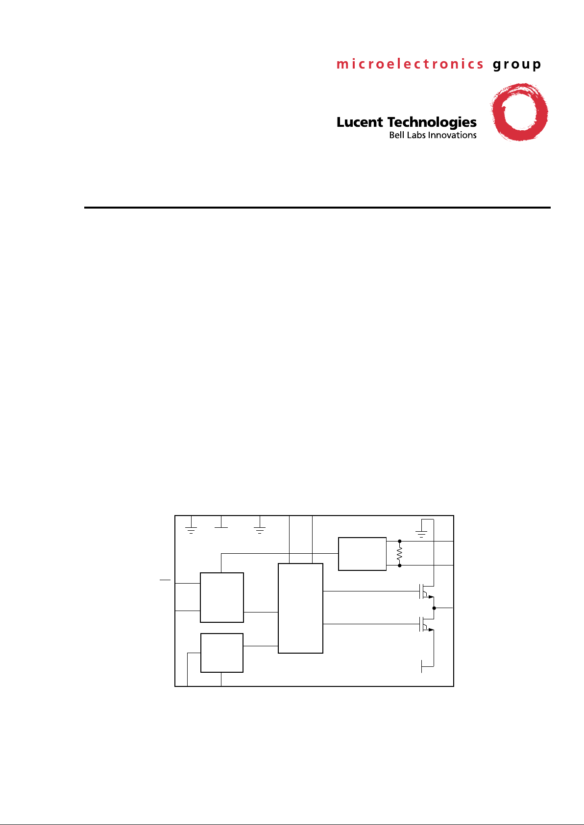
The L7590C Telephone Ringing Driver produces a
low-frequency sinusoidal ringing signal for analog
telephone loops. This is accomplished by producing
an output pulse stream that is an amplified replica of
the digital input. The output is then filtered to produce
a sine wave. The peak-to-peak output level is determined by the magnitude of the negative high-voltage
dc applied to the device (up to –170 V).
The required input is a 100 kHz CMOS-compatible
pulse stream, pulse-width modulated (PWM) at the
desired ringing frequency. The output stage consists
of one upper and one lower drive transistor with an
internal control circuit.
The L7590C IC is optimized for low po wer dissipation
and is available in a 16-pin, surface-mount package.
12-3057a (f)
Figure 1. Block Diagram
CLOCK
CONTROL
LEVEL
SHIFT
AND
OUTPUT
TIMING
CURRENT
LIMIT
BIAS
CIRCUIT
OUT
GNDD
V
DD
CLK
V
REF
VNEG
GNDR
CB1 CB2
EN
30 Ω
L1
L2
VNEG
2 Lucent Technologies Inc.
Data Sheet
June 1998
L7590C Telephone Ringing Driver
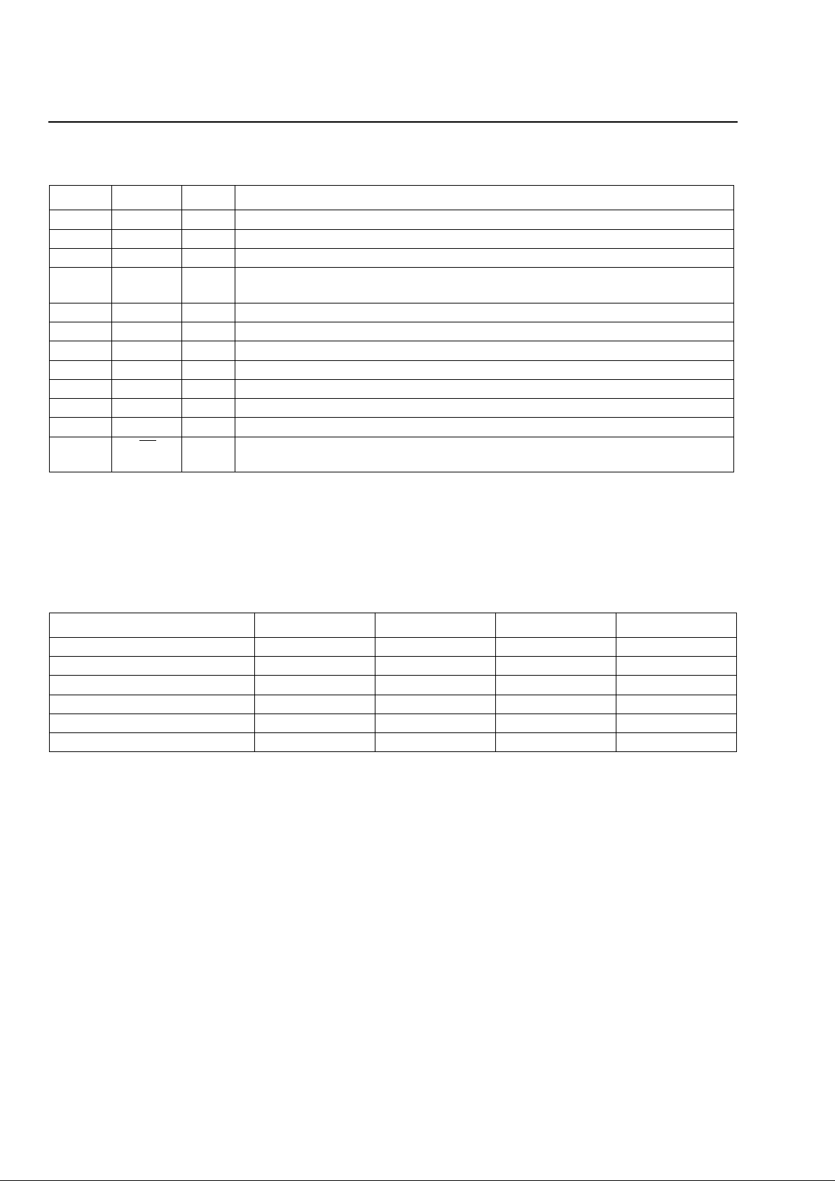
Pin Information
Absolute Maximum Ratings
(T
A
= 25 ° C)
Stresses in excess of the absolute maximum ratings can cause permanent damage to the device. These are absolute stress ratings only. Functional operation of the device is not implied at these or any other conditions in excess
of those given in the operational sections of this data sheet. Exposure to absolute maximum ratings for extended
periods may adversely affect device reliability.
Pin Symbol Type Name/Function
14 V
DD
—
+5 V Power Supply .
3 GNDD — Digital Ground .
12 GNDR — Ringing Ground .
8V
NEG
—
Negative Power Supply . Determines the swing of the ringing generator. Connect
a 1 µ F capacitor from V
NEG
to V
REF
.
5V
REF
—
Internal Reference Voltage . Connect a 1 µ F capacitor from V
REF
to V
NEG
.
16 CLK I
Clock . Modulated pulse stream. Low = 0 V. High = V
DD
.
7 OUT O Ringing Generator Output . Connect to ringing relay contact through a filter.
1 CB1 — Bootstrap Capacitor . Connect a 0.1 µ F capacitor between CB1 and CB2.
2 CB2 — Bootstrap Capacitor . Connect a 0.1 µ F capacitor between CB1 and CB2.
9L1—
Filter Inductor . Connect an inductor to pin L2.
10 L2 — Filter Inductor . Connect an inductor to pin L1.
15
EN
—
Not Enable . A logic lo w activates the internal circuitry. A logic high puts the device
in a low-power powerdown mode.
Parameter Min Typ Max Unit
V
DD
— 7.0 — V
V
NEG
— –200 — V
Timing Input Voltage –0.5 — 7.0 V
Storage Temperature Range –40 — 125
°
C
Maximum Junction Temperature — 150 —
°
C
Relative Humidity Range 5 — 95 %
Lucent Technologies Inc. 3
Data Sheet
June 1998
L7590C Telephone Ringing Driver
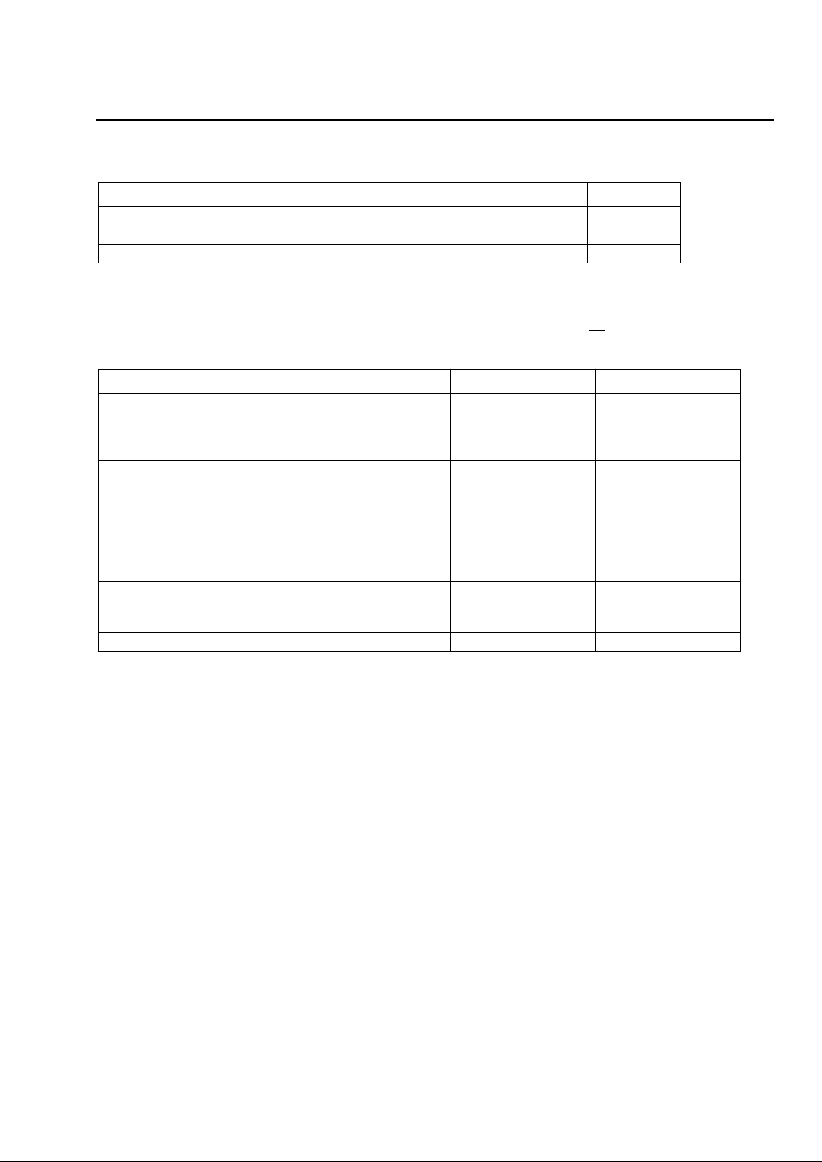
Recommended Operating Conditions
Electrical Characteristics
Electrical characteristics apply for 25 ° C. Unless noted, V
DD
= +5 V, V
NEG
= –170 V,
EN
= low, L1 = 20 mH
(Rdc = 20 Ω , Ceff = 20 pF), CLK = 100 kHz. Positive currents flow into the device. Typical is defined as 25 ° C.
Parameter Min Typ Max Unit
Ambient Temperature –40 — 85
°
C
V
DD
Supply Voltage 4.75 5.0 5.25 V
V
NEG
Supply V oltage –170 — –130 V
Parameter Min T yp Max Unit
Power Supply—Idle (CLK = H or L,
EN
= high, dc):
I
DD
I
NEG
Power Dissipation
—
—
—
—
—
—
1
–50
13.5
mA
µ
A
mW
Power Supply—Active, No Load:
I
DD
I
NEG
Power Dissipation
—
—
—
—
–3.2
—
3
–8
1.38
mA
mA
W
Efficiency =
{[
(V
OUT
)
2
/R
LOAD
]/(V
NEG
•
I
NEG
)
}
:
Sinking Current, R
LOAD
= 1400 Ω Load to GND
Sourcing Current, R
LOAD
= 1400 Ω Load to V
NEG
40
40
80
80
—
—
%
%
ON-resistance:
CLK = H, I
OUT
= –20 mA
CLK = L, I
OUT
= +20 mA
0
0
10
10
20
20
Ω
Ω
Current Limit 25 — 40 mApeak
 Loading...