

AGERE LUCDA4044AAFE Datasheet
Preliminary Data Sheet
August 1998
LUCDA4044 Phase Frequency Detector
Features
■
Typical propagation delay 9.0 ns (through phase
detector)
■
Includes charge pump and amplifier
■
Available in 14-pin DIP or SONB
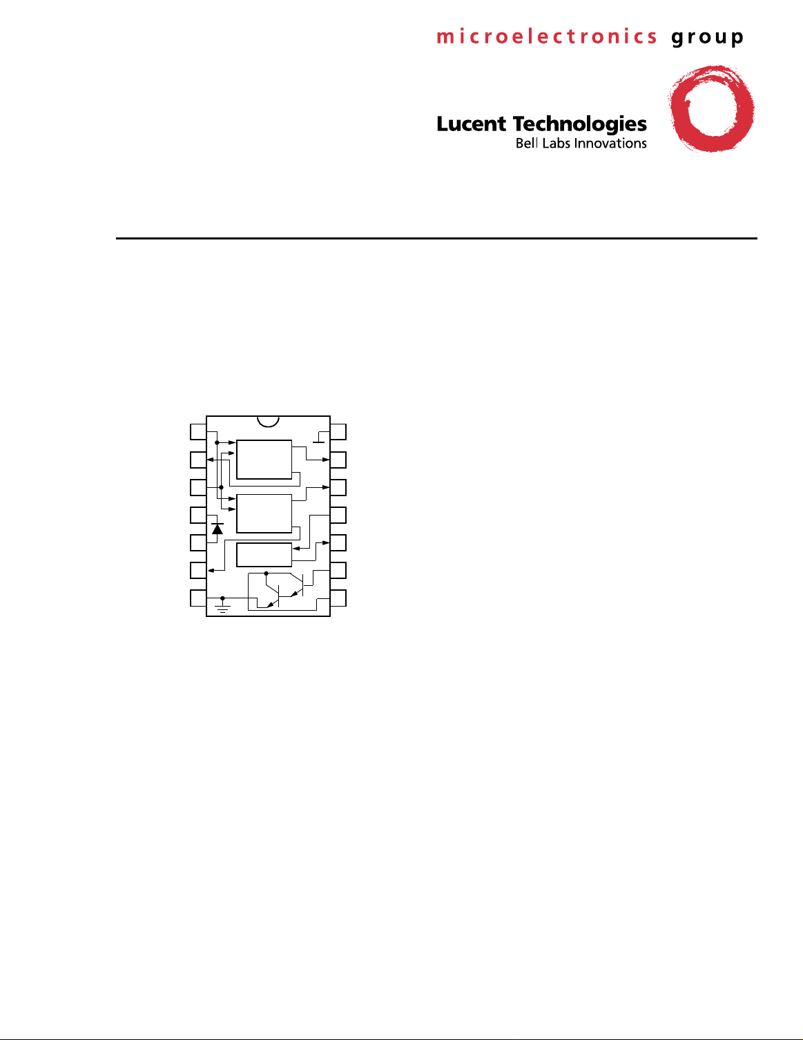
R
1
PHASE
D1
PU
UF
D2
GND
2
V
3
4
5
6
7
FREQUENCY
DETECTOR
#1
PHASE
FREQUENCY
DETECTOR
#2
CHARGE
PUMP
Figure 1. Functional Diagram
V
CC
14
U1
13
U2
12
PD
11
DF
10
AIN
9
AOU
8
12-3519F
Applications
■
Frequency synthesizers
■
Clock recovery
Description
The LUCDA4044 consists of two digital phase detectors, a charge pump, and an amplifier . In combination
with a voltage-controlled multivibrator, this device is
useful in a broad range of phase-locked loop (PLL)
applications. The circuit accepts TTL waveforms at
the R and V inputs and generates an error voltage
that is proportional to frequency and/or phase difference.
Phase detector #1 is intended for use in systems
requiring zero frequency and phase at lock. Phase
detector #2 is used if quadrature lock is desired.
Phase detector #2 can also be used to indicate that
the main loop (utilizing phase detector #1) is out of
lock. This LUCDA4044 is a direct replacement f or the
Motorola
* MC4044.
*
Motorola
is a registered trademark of Motorola Inc.
LUCDA4044 Phase Frequency Detector
Preliminary Data Sheet
August 1998
Pin Information
R
1
D1
2
V
3
PU
4
UF
5
D2
6
GND
7
Figure 2. Pin Diagram
Table 1. Pin Descriptions
Symbol Pin Description
1 R Common Reference Signal Input
2 D1 Detector #1 Output
3 V Common Variable Signal Input
4 PU Diode Cathode
5 UF Diode Anode
6 D2 Detector #2 Output
7 GND Power Supply Ground
8 AOU Amplifier Output
9 AIN Amplifier Input
10 DF Charge Pump Output
11 PD Charge Pump Input
12 U2 Detector #2 Output
13 U1 Detector #1 Output
14 V
Positive Power Supply
CC
14
13
12
11
10
9
8
V
CC
U1
U2
PD
DF
AIN
AOU
12-3518F
Absolute Maximum Ratings
Stresses in excess of the absolute maximum ratings
can cause permanent damage to the device. These are
absolute stress ratings only. Functional operation of the
device is not implied at thes e or any other conditions in
excess of those given in the operational sections of the
data sheet. Exposure to absolute maximum ratings for
extended periods can adversely affect device reliability.
Parameter Symbol Value Unit
Ambient Operating
— –40 to +85 °C
Temperature
Storage Tempera-
T
–40 to +125 °C
stg
ture Range
Power Supply Volt-
age (V
to GND)
CC
— 7.0 V
Truth Table
This table is not strictly a functional truth table; i.e., it
does not show all possible modes of operation. It is
included as an aid for dc testing.
Table 2. Truth Table
Input
State
Input Output
R V U1 D1 U2 D2
1 0 0 x x 1 1
2 1 0 x x 0 1
3 1 1 x x 1 0
4 1 0 x x 0 1
5 0 0 x x 1 1
6 1 0 x x 0 1
7 0 0 0 1 1 1
8 1 0 0 1 0 1
9 0 0 0 1 1 1
10 0 1 0 1 1 1
11 0 0 1 1 1 1
12 0 1 1 1 1 1
13 0 0 1 0 1 1
14 0 1 1 0 1 1
15 0 0 1 0 1 1
16 1 0 1 0 0 1
17 0 0 1 1 1 1
Notes:
x indicates output state unknown.
U1 and D1 outputs are sequential, i.e., they must be sequenced in
the order shown.
U2 and D2 outputs are combinational, i.e., they need only inputs to
obtain the desired output state.
22 Lucent Technologies Inc.
 Loading...