

AGERE LU6612-T64-DB Datasheet

Data Sheet
July 2000
LU6612
for 10Base-T/100Base-TX
FASTCAT
TM
Single-FET
Features
10 Mbits/s Transceiver
■
Compatib le wit h
for twisted-pair cable
■
Autopolarity detection and correction
■
Adjustable squelch level for extended wire line
length capability (2 levels)
■
Interfaces with
interface (MII)
■
On-chip filtering eliminates the need for external filters
■
Half- and full-duplex operations
100 Mbits/s Transceiver
■
Compatib le w ith
(clause 23), PMA (clause 24), autonegotiation
(clause 28), and PMD (clause 25) specifications
■
Scrambler/descrambler bypass
IEEE
* 802.3u 10Base-T standard
IEEE
802.3u media independent
IEEE
802.3u MII (clause 22), PCS
General
■
Autonegotiation (
— Fast link pulse (FLP) burst generator
— Arbitration function
— Accepts preamble suppression
— Operates up to 12.5 MHz
■
Supports the station management protocol and
frame format (clause 22):
— Basic and extended registers
— Supports next-page function
— Accepts preamble suppression
— Operates up to 12.5 MHz
■
Supports the following management functions via
pins if station management is unavailable:
— Speed select
— Encoder/decoder bypass
— Scrambler/descrambler bypass
— Full duplex
— Autonegotiation
■
Supports half- and full-duplex operations
■
Provides four status signals: receive/transmit activity, full duplex, link integrity, and speed indication
IEEE
802.3u clause 28):
■
■
Encoder/decoder bypass
■
3-statable MII in 100 Mbits/s mode
■
Selectable carrier sense signal generation (CRS
asserted during either transmission or reception in
half duplex, CRS asserted during reception only in
full duplex)
■
Selectable MII or 5-bit code group interface
■
Half- or full-duplex o perations
■
On-chip filtering and ada ptive equalizat ion that
Powerdown mode for 10 Mbits/s and 100 Mbits/s
operation
■
Loopback for 10 Mbits/s and 100 Mbits/s operation
■
0.35 µm low-power CMOS technology
■
64-pin TQFP
■
Single 5 V power supply
eliminates the need for external filters
*
IEEE
is a registered trademark of The Institute of Electrical and Electronics Engineers, Inc.
Note: Advisories are issued as needed to update product information. When using this data sheet for design purposes, please contact
your Lucent Technologies Microelectronics Group Account Manager to obtain the latest advisory on this product.

LU6612 Data Sheet
FASTCAT
Single-FET for 10Base-T/100Base-TX July 2000
Table of Contents
Contents Page
Features ....................................................................................................................................................................1
10 Mbits/s Transceiver............................................................................................................................................1
100 Mbits/s Transceiver..........................................................................................................................................1
General ...................................................................................................................................................................1
Description.................................................................................................................................................................4
Pin Information and Descriptions...............................................................................................................................8
MII Station Management ................. ...... ....... ...... ....... ...... ....... ...... ....................................... ....................................13
Basic Operations...................................................................................................................................................13
MII Management Frames......................................................................................................................................13
MODE Selection......................................................................................................................................................23
Absolute Maximum Ratings (T
Electrical Characteristics .........................................................................................................................................24
Timing Characteristics (Preliminary)........................................................................................................................25
Outline Diagram.......................................................................................................................................................34
64-Pin TQFP.........................................................................................................................................................34
Technical Document Types.....................................................................................................................................35
Ordering Information................................................................................................................................................36
A
= 25 °C) ................................................................................................................24
List of Tables
Tables Page
Table 1. MII/Serial Interface Pins (17) ..................................................................................................................... 9
Table 2. MII Management Pins (2) ........................................................................................................................ 10
Table 3. 10/100 Mbits/s Twisted-Pair (TP) Interface Pins (4) ................................................................................ 10
Table 4. Ground and Power Pins (21) ................................................................................................................... 11
Table 5. Miscellaneous Pins (20) .......................................................................................................................... 11
Table 5 . Miscellaneous Pins (20) (continued)....................................................................................................... 12
Table 6. MII Management Frame Fields and Format............................................................................................. 13
Table 7. MII Management Frame Descriptions ...................................................................................................... 13
Table 8. MII Management Registers (MR)............................................................................................................. 14
Table 9. MR0—Control Register Bit Descriptions.................................................................................................. 15
Table 10. MR1—Status Register Bit Descriptions ................................................................................................. 16
Table 11. MR2, 3—PHY Identifier Registers (1 and 2) Bit Descriptions................................................................ 17
Table 12. MR4—Autonegotiation Advertisement Register Bit Descriptions........................................................... 17
Table 13. MR5—Autonegotiation Link Partner (LP) Ability Register Bit Descriptions (Base_Page)...................... 18
Table 14. MR5—Autonegotiation Link Partner (LP) Ability Register Bit Descriptions (Next_Page)....................... 18
Table 15. MR6—Autonegotiation Expansion Register Bit Descriptions................................................................. 19
Table 16. MR7—Next_Page Transmit Register Bit Descriptions............................................................................ 19
Table 17. MR28—Device-Specific Register 1 (Status Register) Bit Descriptions ................................................. 20
Table 18. MR29—Device-Specific Register 2 (100 Mbits/s Control) Bit Descriptions ........................................... 21
Table 19. MR30—Device-Specific Register 3 (10 Mbits/s Control) Bit Descriptions ............................................. 22
Table 20. Operation Modes of LU6612 ................................................................................................................. 23
Table 21. LU6612 Crystal Specifications............................................................................................................... 23
Table 22 . Absolute Maximum Ratings .................................................................................................................. 24
Table 23 . Operating Conditions ............................................................................................................................ 24
Table 24. dc Characteristics................................................................................................................................... 24
Table 25. MII Management Interface Timing (25 pF Load).................................................................................... 25
Table 26. MII Data Timing (25 pF Load)................................................................................................................ 26
Table 27. Serial 10 Mbits/s Timing for RX/RY, CRS, and RX_CLK........................................................................ 28
2 Lucent Technologies Inc.

Data Sheet LU6612
July 2000
FASTCAT
Single-FET for 10Base-T/100Base-TX
Table of Contents
Tables
Table 28. Serial 10 Mbits/s Timing for TX_EN, TX/TY, CRS, and RX_CLK...........................................................28
Table 29. Serial 10 Mbits/s Timing for TX_EN, RX/RY, and COL........................................................................... 29
Table 30. Serial 10 Mbits/s Timing for RX_CLK, CRS, RXD, TX_CLK, TX_EN, and TXD (25 pF Load)............... 30
Table 31. Serial 10 Mbits/s Timing for RX_CLK and TX_CLK (25 pF Load)..........................................................31
Table 32. 100 Mbits/s MII Transmit Timing............................................................................................................. 32
Table 33. 100 Mbits/s MII Receive Timing............................................................................................................. 33
(continued)
(continued)
Page
List of Figures
Figures Page
Figure 1. Functional Block Diagram: Device Overview ............................................................................................ 4
Figure 2. Functional Block Diagram: Device Detail .................................................................................................. 5
Figure 3. Typical Twisted-Pair (TP) Interface........................................................................................................... 6
Figure 4. Onboard Universal Twisted-Pair Interface Circuit to Interchange Lucent and Quality
Semiconductor Inc. Parts.......................................................................................................................... 7
Figure 5. LU6612 Pino ut.................. ...... ....... ...... ....... ...... ....................................... ...... ....... ...... ............................... 8
Figure 6. MDIO Input Timing .................................................................................................................................. 25
Figure 7. MDIO Output Timing ............................................................................................................................... 25
Figure 8. MDIO During TA (Turnaround) of a Read Transaction ........................................................................... 25
Figure 9. MII Timing Requirements for LU6612 ..................................................................................................... 27
Figure 10. Serial 10 Mbits/s Timing for RX/RY, CRS, and RX_CLK ...................................................................... 28
Figure 11. Serial 10 Mbits/s Timing for TX_EN, TX/TY, CRS, and RX_CLK.......................................................... 28
Figure 12. Serial 10 Mbits/s Timing for TX_EN, RX/RY, and COL......................................................................... 29
Figure 13. Serial 10 Mbits/s Timing for RX_CLK, CRS, RXD, TX_CLK, TX_EN, and TXD ................................... 30
Figure 14. Serial 10 Mbits/s Timing Diagram for RX_CLK and TX_CLK................................................................31
Figure 15. 100 Mbits/s MII Transmit Timing ........................................................................................................... 32
Figure 16. 100 Mbits/s MII Receive Timing ............................................................................................................ 33
Lucent Technologies Inc. 3
LU6612 Data Sheet
FASTCAT
Description
The LU6612 is a single-channel, single-chip complete
transceiver designed specifically for dual-speed
10Base-T and 100Base-TX repeaters and switches.
LU6612 implements:
■
The 10Base-T transceiver function of
■
The physical coding sublayer (PCS) of
■
The physical medium attachment (PMA) of
802.3u.
Single-FET for 10Base-T/100Base-TX July 2000
■
IEEE
IEEE
802.3u.
802.3u.
IEEE
Autonegotiation of
■
MII management of
■
Physical medium dependent (PMD) of
This device supports operation over category 3
unshielded twisted-pair (UTP) cable, according to
802.3u 10Base-T specification, and over category 5,
Type 1, UTP and Type 1 shielded twisted-pair cable,
according to
IEEE
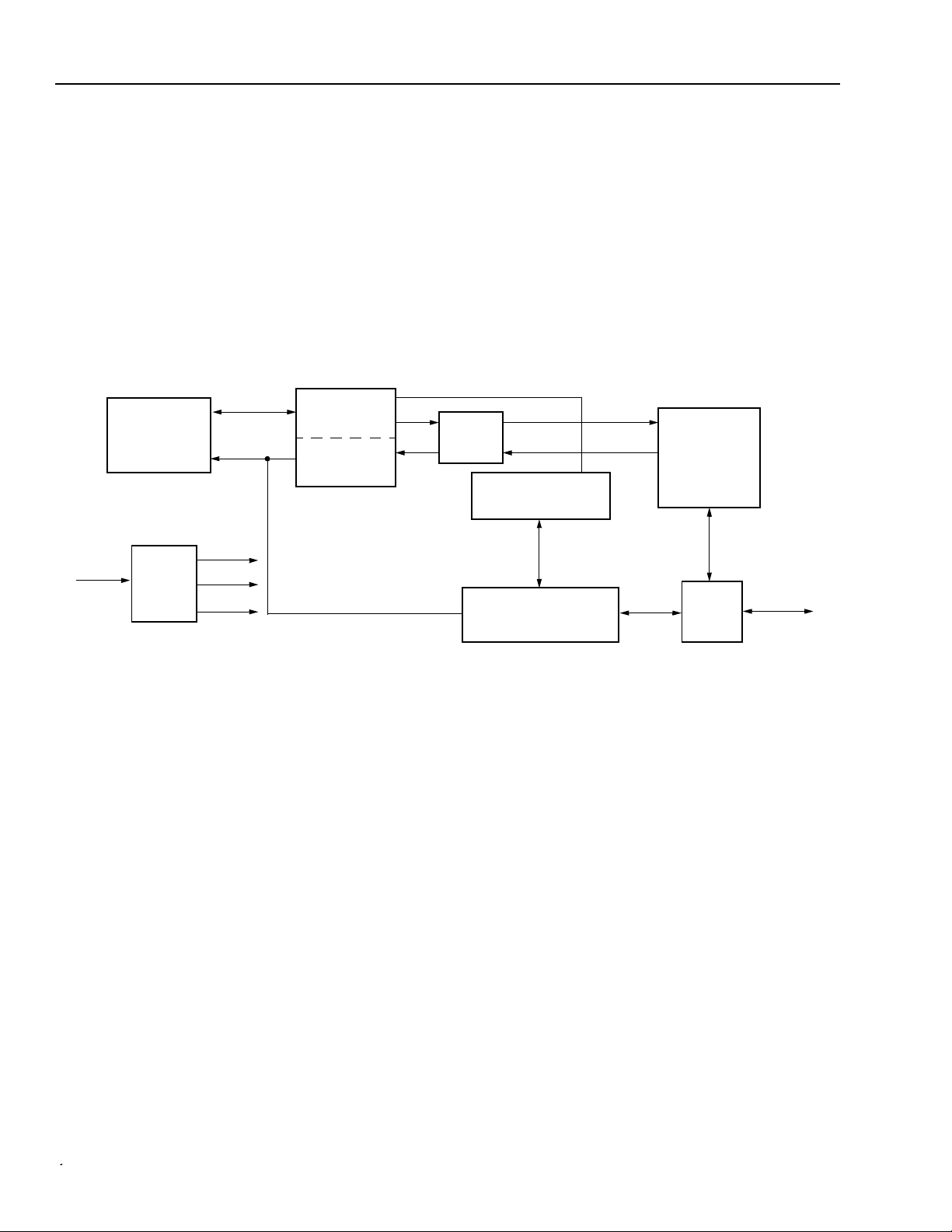
Figure 1 illustrates a functional overview of the LU6612
while Figure 2 details the functions. Figure 3 shows
how the LU6612 interfaces to the twisted pair.
IEEE
802.3u.
IEEE
802.3u.
IEEE
802.3u.
IEEE
802.3u 100Base-X specification.
LSCLK
25 MHz
MII/SERIAL
INTERFACE
DPLL
25 MHz
125 MHz
20 MHz
MANAGEMENT
PMA
PCS
AUTONEGOTIATION
10 Mbits/s TRANSCEIVER
DRIVER AND FILTERS
Figure 1. Functional Block Diagram: Device Overview
TX
PMD
DRIVER AND
FILTERS
MUX
TO/FROM
MAGNETICS
5-5600(F).r1
44 Lucent Technologies Inc.
Data Sheet LU6612
Jul y 200 0
FASTCAT
Single-FET for 10Base-T/100Base-TX
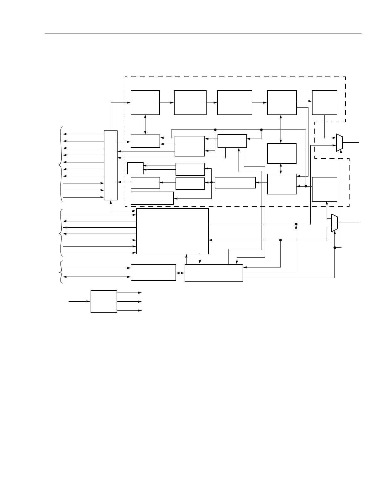
Description
RXD[3:0]
RX_DV
RX_ER/RXD[4]
MII
INTERFACE
SERIAL
INTERFACE
RX_CLK
TX_CLK
TXD[3:0]
TX_EN
TX_ER/TXD[4]
REF10
CLK20
(continued)
TXD[3:0]
CRS
COL
MII
RXC
RXD
TXC
TEN
TXD
100 Mbits/s TRANSCEIVER
4B/5B
ENCODER
TX STATE
MACHINE
CIM
5B/4B
DECODER
FAR-END
FAULT DETECT
10 Mbits/s TRANSCEIVER
SD
CAR_STAT
RXERR_ST
FAR-END
FAULT GEN
COLLISION
DETECT
CARRIER
DETECT
ALIGNER
LC10 LS10
SCRAMBLER
RX STATE
MACHINE
SD
DESCRAMBLER
LC100
LS100
SD
PDT
DCRU
PDR
SD
PMD
TX
PMD
RX
TX/TY
RX/RY
MDC
MDIO
INTERFACE
MANAGEMENT
LSCLK
DPLL
25 MHz
125 MHz
20 MH
MII
MANAGEMENT
Z
AUTONEGOTIATION
AND LINK MONITOR
5-5136(F).cr1
Figure 2. Functional Block Diagram: Device Detail
Lucent Technologies Inc. 5
LU6612 Data Sheet
FASTCAT
Single-FET for 10Base-T/100Base-TX July 2000
Description
(continued)
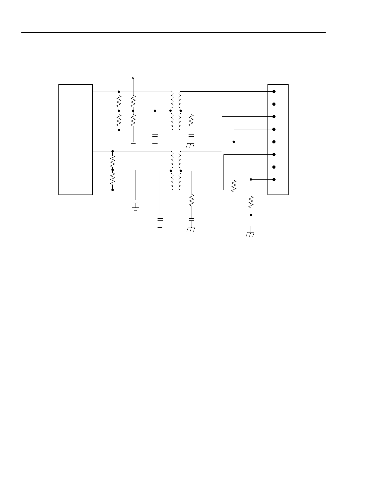
8
9
LU6612
63
64
TX
TY
RX
RY
50
50
Ω
Ω
50
50
0.01 µF
DD
V
1:1
Ω
220
Ω
220
0.01 µF
Ω
Ω
1:1
0.01 µF
Ω
75
0.001 µF
Ω
75
0.001 µF
75
Ω
Ω
75
0.01 µF
RJ-45
1
2
3
4
5
6
7
8
Figure 3. Typical Twisted-Pair (TP) Interface
5-5433.i.r3
6 Lucent Technologies Inc.
Data Sheet LU6612
Jul y 200 0
FASTCAT
Single-FET for 10Base-T/100Base-TX
Description
LU6612
QS6612
(continued)
VDD
TX
8
Q = 86.6
Q = 86.6
TY
9
RX
63
RY
64
Q = 0
Ω
L = OPEN
L = 50
L = 50
Q = 60
L = 50
L = 50
Q = 0
VDD
RJ-45
L = 1:1; Q = 1.25:1
Ω
Ω
Ω
Ω
Ω
Ω
Ω
Ω
L = 0
Q = OPEN
L = 0.01 µF
Q = OPEN
Ω
L = 0
L = 0
Q = 20
Q = 20
L = 0
Q = 20
L = 220
Q = 39
L = 220
Q = OPEN
Ω
Ω
Ω
Ω
Ω
Ω
L = 0.01 µF
Q = 0.1 µF
Ω
Ω
Ω
L = 0.01
Q = 0.1 µF
Ω
L = Q = 1:1
L = Q = 75
L = 0
Q = OPEN
L = Q = 75
Ω
Ω
Ω
Q = 0
Ω
L = OPEN
Q = 0
Ω
L = OPEN
L = 0
Ω
Q = OPEN
L = Q = 75
Ω
L = Q = 75
L = 0.01 µF
Q = 1000 pF
1
2
3
4
5
6
7
8
Ω
Key:
L = Lucent’s LU6612.
Q = Quality Semiconductor Inc. QS6612.
Figure 4. Onboard Universal Twisted-Pair Interface Circuit to Interchange Lucent and
Quality Semiconductor Inc. Parts
L = 0.001 µF L = 0.001 µF
5-5433.j
Lucent Technologies Inc. 7

LU6612 Data Sheet
FASTCAT
Single-FET for 10Base-T/100Base-TX July 2000
Pin Information
VCCBG
ISET_100
GNDBG
LINKLED/PHYAD[0]
ACTLED/PHYAD[1]
CC
V
IOA
GNDIOA
TX
TY
GNDT
CC
V
CLKREF
GNDBT
CC
V
BT
TEST[0]
TEST[1]
REC
EQAP
CC
CC
V
V
RY
RX
GNDEQAP
60
61
62
63
64
1
2
3
4
5
6
7
8
9
10
11
T
12
13
14
15
16
17
18
19
20
21
GNDREC
59
22
BGREF[1]
BGREF[0]
57
58
LU6612
23
24
IOB
CC
MODE[2]
GNDIOB
V
FUDUPLED/PHYAD[3]
SPEEDLED/PHYAD[2]
52
53
54
55
56
25
26
27
28
29
DIGB
CC
MODE[0]
MODE[1]
V
49
50
51
30
48
GNDDIGB
47
TX_CLK
46
RX_ER/RXD[4]
45
RX_DV
44
RX_CLK
43
COL
42
CRS
41
GNDIOC
40
RXD[0]
39
RXD[1]
38
RXD[2]
37
RXD[3]
36
GNDDIGA
35
34
33
31
32
CC
V
DIGA
TXD[0]
TXD[1]
PLL
CC
PCSEN
V
TEST[2]
LSCLK1
LSCLK2
PHYAD[4]
GNDPLL
MDIO
ISET_10
MDC
RESET
RX_EN
TX_EN
TXD[3]
TXD[2]
TX_ER/TXD[4]
5-5866.r2
Figure 5. LU6612 Pinout
8 Lucent Technologies Inc.

Data Sheet LU6612
Jul y 200 0
FASTCAT
Single-FET for 10Base-T/100Base-TX
Pin Information
(continued)
Pin Descriptions
Table 1. MII/Serial Interface Pins (17)
Signal Type Pin Description
COL O 43
CRS O 42
RX_CLK O 44
RXD[3:0] O 37:40
RX_DV O 45
RX_ER/
O46
RXD[4]
TX_CLK O 47
TXD[3:0] I 31:34
TX_EN I 30
Collision Detect.
This signal signifies in half-duplex mode that a collision has
occurred on the network. COL is asserted high whenever there is transmit and
receive activity on the UTP media. COL is the logical AND of TX_EN and receive
activity , and is an asynchronous output. When SERIAL_SEL (register 30, bit 1) is high
and in 10Base-T mode, this signal indicates the jabber timer has expired. This signal
is held low in full-duplex mode.
Carrier Sense.
When CRS_SEL (register 29, bit 10) is low, CRS is asserted high
when either the transmit or receive is nonidle. This signal remains asserted throughout a collision condition. When CRS_SEL (register 29, bit 10) is high, CRS is
asserted on receive activity only.
Receive Clock.
25 MHz clock output in 100 Mbits/s mode, 2.5 MHz output in
10 Mbits/s nibble mode, 10 MHz in 10 Mbits/s serial mode. RX_CLK has a worst-case
45/55 duty cycle. RX_CLK provides the timing reference for the transfer of RX_DV,
RXD, and RX_ER signals.
Receive Data.
4-bit parallel data outputs that are synchronous to the falling edge of
RX_CLK. When RX_ER is asserted high in 100 Mbits/s mode, an error code will be
presented on RXD[3:0] where appropriate. The codes are as follows:
■
Packet errors: ERROR_CODES = 2h;
■
Link errors: ERROR_CODES = 3h (Packet and link error codes will only be
repeated if registers [29.9] and [29.8] are enabled.);
■
Premature end errors: ERROR_CODES = 4h;
■
Code errors: ERROR_CODES = 5h.
When SERIAL_SEL (register 30, bit 1) is active-high and 10 Mbits/s mode is selected,
RXD[0] is used for data output and RXD[3:1] are 3-stated.
Receive Data Valid.
When this pin is high, it indicates the LU6612 is recovering and
decoding valid nibbles on RXD[3:0], and the data is synchronous with RX_CLK.
RX_DV is synchronous with RX_CLK. This pin is not used in serial 10 Mbits/s mode.
Receive E rr or.
When high, RX_ER indicates the LU6612 has detected a coding error
in the frame presently being transferred. RX_ER is synchronous with RX_CLK. When
the encode/decode bypass (EDB) is selected through the MII management interface,
this output serves as the RXD[4] output. This pin is only valid when LU6612 is in
100 Mbits/s mode.
Transmit Clock.
25 MHz clock output in 100 Mbits/s mode, 2.5 MHz output in
10 Mbits/s MII mode, 10 MHz output in 10 Mbits/s serial mode. TX_CLK provides timing reference for the transfer of the TX_EN, TXD, and TX_ER signals. These signals
are sampled on the rising edge of TX_CLK.
Transmit Data.
4-bit parallel input synchronous with TX_CLK. When SERIAL_SEL
(register 30, bit 1) is active-high and 10 Mbits/s mode is selected, only TXD[0] is valid.
Transmit Enable.
When driven high, this signal indicates there is valid data on
TXD[3:0]. TX_EN is synchronous with TX_CLK. When SERIAL_SEL
(register 30, bit 1) is active-high and 10 Mbits/s mode is selected, this pin indicates
there is valid data on TXD[0].
Lucent Technologies Inc. 9

LU6612 Data Sheet
FASTCAT
Single-FET for 10Base-T/100Base-TX July 2000
Pin Information
Table 1. MII/Serial Interface Pins (17)
Signal Type Pin Description
TX_ER/
TXD[4]
RX_EN I 28
Table 2. MII Management Pins (2)
Signal Type Pin Description
MDC I 26
MDIO IO 25
(continued)
I29
Transmit Coding Error.
tionally corrupt the byte being transmitted across the MII (00100 will be transmitted).
When the encoder/decoder bypass bit is set, this input serves as the TXD[4] input.
When in 10 Mbits/s mode and SERIAL_SEL (register 30, bit 1) is active-high, this pin
is ignored.
Receive Enable.
RX_DV) are enabled. This pin has an internal 100
Management Data Clock.
the MDIO signal. This signal may be asynchronous to RX_CLK and TX_CLK. The
standard clock rate is 2.5 MHz, the maximum clock rate is 12.5 MHz. When running
MDC above 6.25 MHz, MDC must be synchronous with LSCLK and have a setup time
of 15 ns and a hold time of 5 ns with respect to LSCLK.
Management Data Input/Output.
mation between LU6612 and the station management. Control information is driven by
the station management synchronous with MDC. Status information is driven by the
LU6612 synchronous with MDC.
(continued)
When driven high, this signal causes the encoder to inten-
When this pin is high, the outputs (RXD[3:0], RX_ER, RX_CLK,
This is the timing reference for the transfer of data on
This I/O is used to transfer control and status infor-
Ω
pull-up resistor.
k
Table 3. 10/100 Mbits/s Twisted-Pair (TP) Interface Pins (4)
Signal Type Pin Description
RX I 63
RY I 62
TX O 8
TY O 9
Received Data.
Manchester data from magnetics.
Received Data.
Manchester data from magnetics.
Transmit Data.
Manchester data to magnetics.
Transmit Data.
Manchester data to magnetics.
Positive differential received 125 Mbaud MLT3 or 10 Mbaud
Negative differential received 125 Mbaud ML T3 or 10 Mbaud
Positive differential transmit 125 Mbaud MLT3 or 10 Mbaud
Negative differential transmit 125 Mbaud MLT3 or 10 Mbaud
10 Lucent Technologies Inc.

Data Sheet LU6612
g
[0]
[0]
g
g
y
y
[1]
[1]
g
g
Jul y 200 0
FASTCAT
Single-FET for 10Base-T/100Base-TX
Pin Information
(continued)
Table 4. Ground and Power Pins (21)
Signal Type Pin Description
IOA PWR 6 Digital +5 V power supply for I/O
V
CC
GNDIOA PWR 7 Digital ground for I/O
V
IOB PWR 54 Digital +5 V power supply for I/O
CC
GNDIOB PWR 53 Digital ground for I/O
GNDIOC PWR 41 Digital ground for I/O
V
DIGA PWR 35 Digital +5 V power supply for logic
CC
GNDDIGA PWR 36 Digital ground for logic
V
DIGB PWR 49 Digital +5 V power supply for logic
CC
GNDDIGB PWR 48 Digital ground for logic
V
REC PWR 60 Digital +5 V power supply for clock recovery circuit
CC
GNDREC PWR 59 Digital ground for clock recovery circuit
V
PLL PWR 20 Analog +5 V power supply for 10 MHz and 100 MHz PLL clock synthesizer
CC
GNDPLL PWR 23 Analog ground for 10 MHz and 100 MHz PLL clock synthesizer
V
T PWR 11 Analog +5 V power supply for transmitter
CC
GNDT PWR 10 Analog ground for transmitter
V
EQAP PWR 61 Analog +5 V power supply for equalizer and adaptation circuit
CC
GNDEQAP PWR 64 Analog ground for adaptation circuit.
V
BG PWR 1 Analog +5 V power supply for band-gap circuit
CC
GNDBG PWR 3 Analog ground band-gap circuit
V
BT PWR 14 Analog +5 V power supply for 10Base-T transmitter
CC
GNDBT PWR 13 Analog ground for 10Base-T transmitter
Table 5. Miscellaneous Pins (20)
Signal Type*Pin Description
LSCLK1 I 21
Local Symbol Cl ock.
25 MHz clock, ±100 ppm, 40%—60% duty cycle. This input is
connected to one terminal of a 25 MHz crystal or an external 25 MHz clock source.
LSCLK2 O 22
Local Symbol Clock.
25 MHz crystal feedback. This output is connected to the
other terminal of a 25 MHz crystal or an external 25 MHz. If LSCLK1 is driven from
an external clock source, LSCLK2 is left unconnected.
LINKLED/
PHYAD[0]
ACTLED/
PHYAD[1]
↑
*
indicates there is an internal pull-up; ↓ indicates there is an internal pull-down.
I/O 4
I/O 5
Link LED.
This pin indicates
as input and to set the PHYAD
PHYAD
to a high or if pulled low through a resistor, will set PHYAD[0] to a zero.
When this pin is pulled hi
LED output will be active-hi
Activit
LED.
This pin indicates transmit/receive activit
ood link status. At powerup/reset, this pin is sampled
bit. If pulled high through a resistor, this pin will set
h the LED output will be active-low, when pulled low the
h.
is sampled as input to set the PHYAD
will set PHYAD
zero. When this pin is pulled hi
the LED output will be active-hi
to a high or if pulled low through a resistor, will set PHYAD[1] to a
h the LED output will be active-low, when pulled low
h.
. At powerup/reset, this pin
bit. If pulled high through a resistor, this pin
Lucent Technologies Inc. 11
 Loading...