

AGERE LU5X34F Datasheet

Preliminary Data Sheet
(
)
g
q
g
July 2000
Overview
The LU5X34F is a low-cost, low-power quad transceiver. It is used for data transmission over fiber or
IEEE
coaxial media in conformance with
Gigabit Ethernet specification and Fibre Channel
†
ANSI
X3T11 at 1.0 Gbits/s and
1.25 Gbits/s.
Each of the four transceivers independently provides
complete serialize/deserialize (SERDES) and transmit and receive functions. The device is available in a
217-pin PBGA package.
The transmitter section accepts TTL compatible data
at the 10-bit parallel input port. The parallel input
data is latched on the rising edge of TXCLKx. It also
accepts the low-speed, TTL compatible system
clock, REFCLK, and uses this clock to synthesize the
internal high-speed serial bit clock. The serialized
data is then available at the differential PECL outputs, terminated in 50 Ω or 75 Ω to drive eit her an
optical transmitter or coaxial media.
The receive section receives high-speed serial data
at its differential PECL input port. This data is fed to
the digital clock recovery section, which generates a
recovered clock and retimes the data. The retimed
data is deserialized and presented as 10-bit parallel
data on the output port. A divided-down version of
the recovered clock, synchronous with parallel data
bytes, is also available as a TTL compatible output.
The receive section recognizes the comma character
and aligns the comma-containing byte on the word
boundary, when ENCDET = 1.
* 802.3z
LU5X34F
Quad Gigabit Ethernet Transceiver
■
100 MHz—125 MHz differential or single-ended
reference clock.
■
10-bit parallel,
■
8-bit/10-bit encoded data.
■
High-speed comma character recognition (K28.1,
K28.5, K28.7
and ali
■
Two 50 MHz—62.5 MHz receive-byte clocks.
■
Single analog PLL design requires no external
nment to word boundary.
components for the fre
■
Novel digital data lock in receiver avoids the need
for multiple analo
■
Expandable beyond four serializer/deserializers.
■
PECL high-speed interface I/O for use with optical
TTL-compatible I/O interface
for latency-sensitive applications
uency synthesizer.
PLLs.
transceiver or coaxial copper media.
■
Requires one external resistor for PECL output reference-level definition.
■
Low-power digital CMOS technology.
■
Less than 2 W total power dissipation per quad
transceiver.
■
3.3 V ± 5% power supply.
■
0 °C—
70 °C ambient temperature.
■
Stand-alone transceiver product.
■
Transceiver ma crocell templat e.
■
Available in 217-pin PBGA package.
.
Features
■
Designed to operate in Ethernet, fibre channel,
Firewire
■
Operationally compliant to
Ethernet specification.
■
Operationally compliant to Fibre Channel
X3T11. Provides FC-0 services at 1.0
1.25 Gbits/s
‡
, or backplane applications.
10-bit encoded data rate).
IEEE
802.3z Gigabit
ANSI
Gbits/s—
*
IEEE
is a registered trademark of The Institute of Electrical and
Electronics Engineers, Inc.
†
ANSI
is a registered trademark of American National Standards
Institute.
‡
FireWire
is a registered trademark of Apple Computer, Inc.

LU5X34F Preliminary Data Sheet
Quad Gigabit Ethernet Transceiver July 2000
Table of Contents
Contents Page Table Page
Overview....................................................................1
Features.....................................................................1
Functional Description .................................. ...... .......3
Transmitter Section.................................... ...... .......3
Receiver Section.....................................................3
Lock to Reference...................................................3
Byte Alignment........................................................4
Parallel Output Port.................................................4
Loopback Mode Operation..... ....... ...... ....... .............4
Powerup Sequence.................................................5
Device Reset...........................................................5
Sleep Mode.............................................................5
Block Diagrams.......................................................6
Block Diagrams (continued)....................................7
Input/Output Information ............................................8
Electrical Specifications ...........................................14
Transmitter............................................................14
Receiver................................................................14
Receiver (continued).............................................15
Timing Characteristics .............................................16
Serial Timing.........................................................16
Receiver Section Timing.......................................17
Receiver Port Timing.............................................17
Transmitter Section Timing .... ....... ...... ....... ...........18
Application Section ..................................................19
Test Modes ..............................................................22
Outline Diagram.......................................................24
217-pin PBGA.......................................................24
Ordering Information................................................25
Table 1. Receive Circuit Operating Modes .............3
Table 2. Definition of Bit Transmission/Reception
Order ....................................................................4
Table 3a. Pinout—Channel A I/O............................9
Table 3b. Pinout—Channel B I/O..........................10
Table 3c. Pinout—Channel C I/O..........................11
Table 3d. Pinout—Channel D I/O .........................12
Table 3e. Pinout—Common I/O............................13
Table 3f. Pinout—Power I/O .................................13
Table 4. Reference Clock Specifications
(REFCLK and REFCLKN) ..................................14
Table 5. PLL Specifications ..................................14
Table 6. Output Jitter at 1.0 Gbit/s—1.25 Gbits/s
Data Rate ...........................................................14
Table 7. Input Data Rate.......................................14
Table 8. Data Lock Characteristics.......................14
Table 9. Power Dissipation ...................................15
Table 10. dc Electrical Specifications ...................15
Table 11. Absolute Maximum Ratings ..................15
Table 12. Serial Output Timing Levels..................16
Table 13. Serial Input Interface Timing ................16
Table 14. Receiver Parallel Port Timing ...............17
Table 15. Transmitter Timing at Parallel Interface 18
Table 16. External Resistor Value vs. Differential
Output Level Viewing ............................. ............20
Table 17. External Resistor Value vs. Differential
Output Level Viewing ............................. ............21
Table 18. Test Modes ...........................................22
Figure Page
Figure 1. LU5X34F Quad Gigabit Ethernet Transceiver
Block Diagram........................................................ 6
Figure 2. LU5X34F Single-Channel Transceiver Func-
tional Diagram ........................................................ 7
Figure 3. Pin Designations (Top View) ..................... 8
Figure 4. Serial Interface Timing............................. 16
Figure 5. Receiver Section Timing.......................... 17
Figure 6. Receiver Port Timing ............................... 17
Figure 7. Parallel Interface Transmit Timing........... 18
Figure 8. Reference Clock Connections with Single-
Ended and Differential Sources............................ 19
Figure 9. Typical Termination for a Single-Channel,
High-Speed Serial Transmit-and-Receive Port in a
50 Ω Backplane Application ................................. 20
Figure 10. Typical Termination for a Single-Channel,
High-Speed Serial Transmit Port Interfacing a 5 V
GBIC Transceiver................................................. 21
2
Lucent Technologies Inc.

Preliminary Data Sheet LU5X34F
g
g
g
g
July 2000 Quad Gigabit Ethernet Transceiver
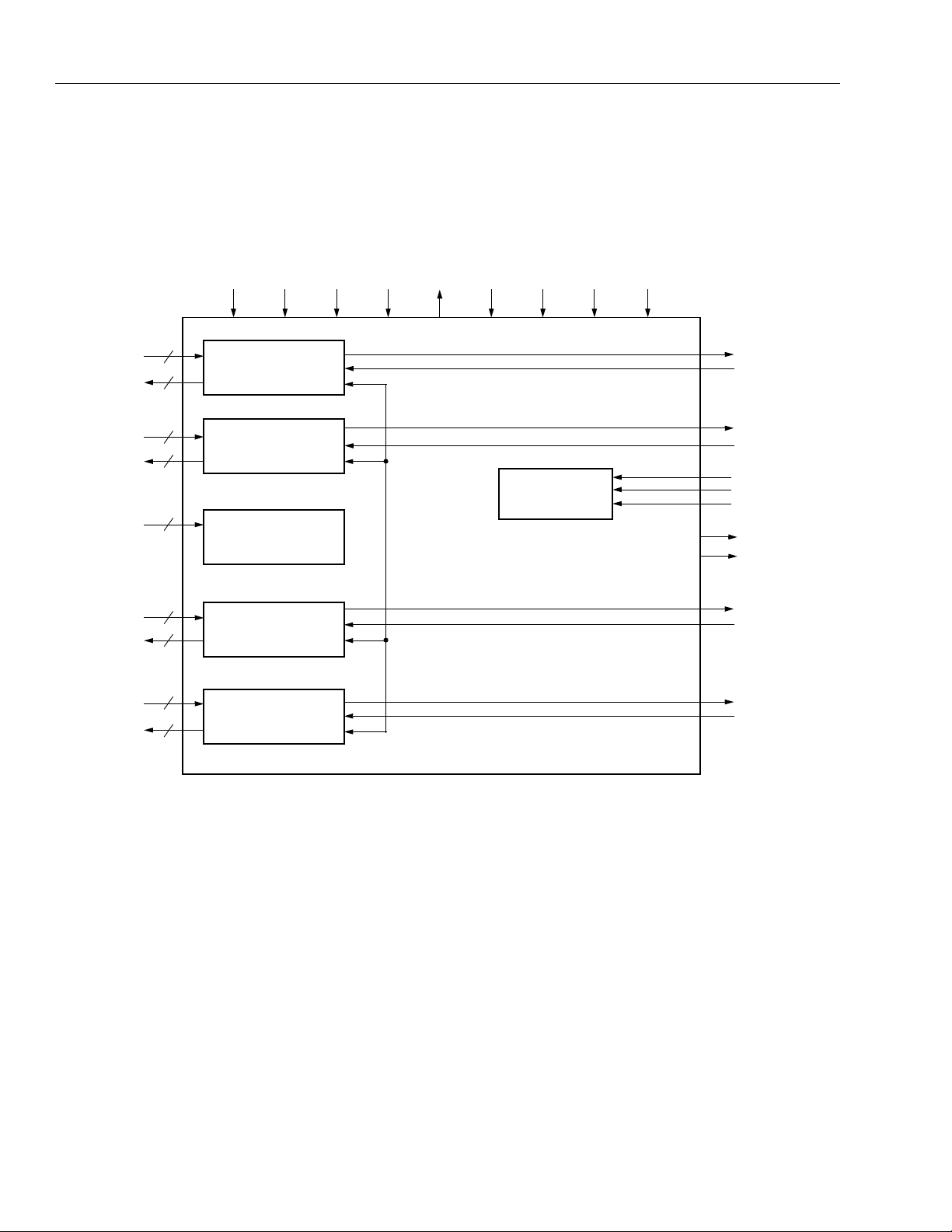
Functional Description
The LU5X34F transceiver provides for data transmission over fiber or coaxial media at 1.0 Gbits/s to
1.25 Gbits/s. The block dia
is shown in Fi
pinout for the 217-pin PBGA packa
Fi
ure 3 and Table 3
ure 1 and the four-channel applica tion
.
Transmitter Section
The transmitter accepts 8b/10b encoded bits in 10-bit
parallel form and converts to serial format for up to
1.25 Gbits/s transmission. The serial nonreturn to zero
(NRZ) bits are then shifted out of the device at a maximum rate of 1.25 Gbits/s. Internally, the device uses
two parallel shift registers that operate at half rate (i.e.,
a maximum of 625 MHz) for reduced power consumption. The two shift registers drive the PECL output
buffer in an interleaved manner to construct the
1.25 Gbits/s output data stream.
The typical transmit-and-receive, high-speed I/O inter-
facing for a single-channel backplane application is
shown in Figure 9.
The transmit shift register and other circuits are driven
with clocks generated from a 500 MHz—625 MHz internal clock. This internal clock is sourced from a voltagecontrolled oscillator (VCO) that is locked to the external
reference of 100 MHz—125 MHz. The internal transmit
phase- lock loop multiplies the frequency of the input
reference clock by a factor of 5, and controls the transmit jitter bandwidth with appropriate design of the jitter
transfer function. The transmit phase-lock loop generates multiple clock phases that are all used by each of
the four receiver circuits. The clock phases are derived
from the transmit VCO.
ram of the quad transceiver
e is given in
Receiver Section
Each of the quad receiver circuits recovers clock from
and retimes the serial input data. The data is input to
the receiver on differential PECL buffers. External termination resistors are supplied by the user in accordance with
differential inputs, HDINP and HDINN, are ac-coupled
to the device and internally biased to the PECL input
common-mode range center. See Figure 9 for the typical application and termination of the transmission
lines.
The receiver data-retiming circuit uses a digital timing
recovery loop that compares the phase of the input
data to multiple phases of the on-device VCO in the
transmit section. One of the phases is chosen to retime
the receive data. A digital low-pass filter is used in the
timing recovery loop to reject jitter from the data input.
A novel phase interpolation circuit permits the retiming
clock’s phase to be stepped with fine resolution for precise alignment of the sampling clock within the data
eye. Use of this digital data locking scheme for each
receiver advantageously avoids the use of multiple
analog phase-lock loops on-device that can potentially
injection lock to one another. Additionally, the digital
data locking loop maintains precise loop dynamics,
hence, the jitter transfer function is process and temperature independent.
ANSI
standard, X3T11. The serial
Lock to Reference
The receive circuit has two modes of operation: lock to
reference, and lock to data with retiming. When no data
or invalid data is present on the HDINP and HDINN
input pins, the user can program the device to ignore
the input data by setting LCKREFN equal to logic 0. In
this mode, neither the PECL input buffer nor the RX
parallel data bus toggles. In normal operation, the
LCKREFN is a logic 1 and the receiver attempts to lock
to the incoming data. If the input data is invalid or outside the nominal ± frequency range, the receive digital
PLL will simply ramp the phase of the output clock until
it locks to data.
Table 1. Receive Circuit Operating Modes
Mode Lock to Reference Lock to Receive Data
LCKREFN = 1 (normal operation) Not applicable. Continually attempts to lock to
LCKREFN = 0 Lock to clock, output data does not
* REFCLK requirements are given in Table 4, and receive PLL specifications are given in Table 5.
Lucent Technologies Inc.
*
data.
Not applicable.
toggle. Disable PECL input buffer.
3

LU5X34F Preliminary Data Sheet
g
y
y
g
g
(
y
y
g
Quad Gigabit Ethernet Transceiver July 2000
Functional Description
(continued)
Byte Alignment
When ENCDET = 1, the LU5X34F recognizes the
comma character and ali
word boundar
COMDET =1 when the parallel output word contains a
te-aligned comma character. The COMDET flag will
b
continue to pulse a lo
comma character is at the parallel output port, independent of ENCDET. When ENCDET = 0, there are two
possible scenarios dependin
character is received.
1. If byte alignment had been previously achieved when
ENCDET had been a logic 1, the COMDET flag will
continue to pulse a logic 1 whenever a byte-aligned
comma character is at the parallel output port. If a
comma character occurs that is not on the word
boundary, no attempt will be made to align this
comma character and the COMDET flag will remain
at a logic 0.
2. If byte alignment had
when ENCDET had been a logic 1, then the first
(and only the first) comma character received will be
aligned to the word boundary. COMDET will pulse
when the comma character is aligned to the word
boundary.
, bits RX[0:9].
ns this 10-bit character to the
ic 1 whenever a byte-aligned
upon when the comma
not
been previously achieved
Parallel Output Port
Timing for the parallel output data and the 50 MHz to
62.5 MHz receive-byte clock is given in Table 14.
Two low data rate receive-byte clocks are available as
TTL compatible outputs during use of the parallel output port in 10-bit mode. RXCLK1 is the receive byte
clock used by the protocol device to register bytes 0
and 2. RXCLK0 is the receive-byte clock used by the
protocol device to register bytes 1 and 3, and it is
180 degrees out of phase with RXCLK1. Both RXCLK1
and RXCLK0 can be stretched during byte alignment
but not truncated or slivered. The maximum allowable
frequency of these two clocks under all circumstances,
excluding start-up, will not exceed 80 MHz. The startup time is specified as 1 ms.
Loopback Mode Operation
A control signal input, EWRAP, selects between two
possible sets of inputs: normal data
internal loopback data. When EWRAP = 1, the serial
output ports, HDOUTP and HDOUTN, remain active.
The serial transmit data prior to the PECL output driver
is directed to the data recover
recovered and data is res
clock. Retimed data and clock then
parallel converter
.
nchronized to the recovered
HDINP, HDINN) or
circuit, where clock is
o to the serial-to-
Table 2. Definition of Bit Transmission/Reception Order
Serial Transmit/
Receive Rate
1.0 Gbits/s to 1.25 Gbits/s TX
* Lower case X signifies channel A, B, C, or D.
[0] bit serially transmitted first at
X
HDOUT
X
TXX[9:0] RXX[9:0]
P, HDOUTXN
*
[0] bit received first at serial inputs
RX
X
HDIN
P, HDINXN
X
4
4
Lucent Technologies Inc.

Preliminary Data Sheet LU5X34F
g
g
g
g
g
q
g
g
y
g
y
g
g
y
g
q
g
July 2000 Quad Gigabit Ethernet Transceiver
Functional Description
(continued)
Powerup Sequence
The power ramp time for the LU5X34F is specified at
DD
V
> 2.7 V within 20 µs of start-up. Once 2.7 V is
reached, the device is held in reset for 15 µs—70 µs.
The REFCLK mu st be ac tive a nd wit hin spec ific atio n at
this point and remain active while the device is powered up, unless in Reset.
When si
the followin
1. 0 µs—32 µs, the analog PLL is held at minimum fre-
quency to allow dc bias to settle.
2. 32 µs—262 µs, the analog PLL has locked-in and
receiver analog circuits start to lock-in.
3. 262 µs—326 µs, the receiver analog circuits are
locked; receiver starts to lock onto incoming data.
4. After 358 µs, the receiver is locked onto incoming
data and can be viewed at the parallel output ports.
The comma-detect circuit is enabled at this point,
allowing byte alignment if ENCDET = 1.
nals RESET, BYPPLL, and LPWR are all low,
start-up sequence occurs:
Sleep Mode
The LU5X34F has a sleep mode that is activated by
enablin
of the REFCLK is used to refresh the d
within the transceiver. The PLL is powered down in this
mode also. LCKREFN can also be activated to reduce
the power even further. Note that complete powerdown
for I
lo
ceiver. The lock-in se
comin
LPWR. In this mode, a divided-down version
namic circuits
DD
Q testing is not supported due to the dynamic
ic used in the high-speed sections of the trans-
uence timing is needed when
out of sleep mode.
If LCKREFN goes low after the 358 µs, the receiver will
sit idle. When LCKREFN goes high, the receiver will be
locked onto data after 2 µs.
Device Reset
The RESETN input to the device is active-low.
activated with a pulse duration of 1 µs, the RESETN si
nal
lobally resets the device a nd th e follow ing is per-
:
formed
1.
The sin
mum fre
be locked in this condition
2. The HDOUTP, HDOUTN outputs are forced to a
PECL logic 0.
3.
The deserializer clocks, but input data at HDINP,
HDINN is i
their previous state
4. T
he phase interpolation/se lection circu its are deact i-
vated and the selecte d pha se i s r eset.
5.
The receiver di
Normall
althou
PLL circuitr
hi
le analog PLL is forced to operate at the mini-
uency possible for its VCO. The PL L w ill not
.
nored and the RX[9:0] signals remain in
.
ital low-pass filter in the DPLL is r eset.
, a reset is not necessa ry for correct ope ration,
h a reset can aid rapid lock-in of the inter nal
. This active-low pin is internally pulled
.
h
When
-
Lucent Technologies Inc.
5
LU5X34F Preliminary Data Sheet
Quad Gigabit Ethernet Transceiver July 2000
Functional Description
Block Diagrams
LPWR RESET
HDINAP
HDINAN
HDOUTAP
HDOUTAN
HDINBP
HDINBN
HDOUTBP
HDOUTBN
REFCLK
REFCLKN
2
2
2
2
2
TRANSCEIVER A
TRANSCEIVER B
ANALOG PLL
(continued)
TXCLK[A:D]*
ENCDET[A:D]
COMDET[A:D]
EWRAP[A:D]
LCKREFN[A:D]
TEST CIRCUITS
OLREF OLRVS
RXA[9:0]
TXA[9:0]
RXB[9:0]
TXB[9:0]
TEST[5:1]
LDST[A:D]
BYPPLL
RXCLK0[A:D]
RXCLK1[A:D]
HDINCP
HDINCN
HDOUTCP
HDOUTCN
HDINDP
HDINDN
HDOUTDP
HDOUTDN
* Synchronous with REFCLK(N).
2
2
2
2
Figure 1. LU5X34F Quad Gigabit Ethernet Transceiver Block Diagram
TRANSCEIVER C
TRANSCEIVER D
RXC[9:0]
TXC[9:0]
RXD[9:0]
TXD[9:0]
5-8808(F)
6
Lucent Technologies Inc.
Preliminary Data Sheet LU5X34F
July 2000 Quad Gigabit Ethernet Transceiver
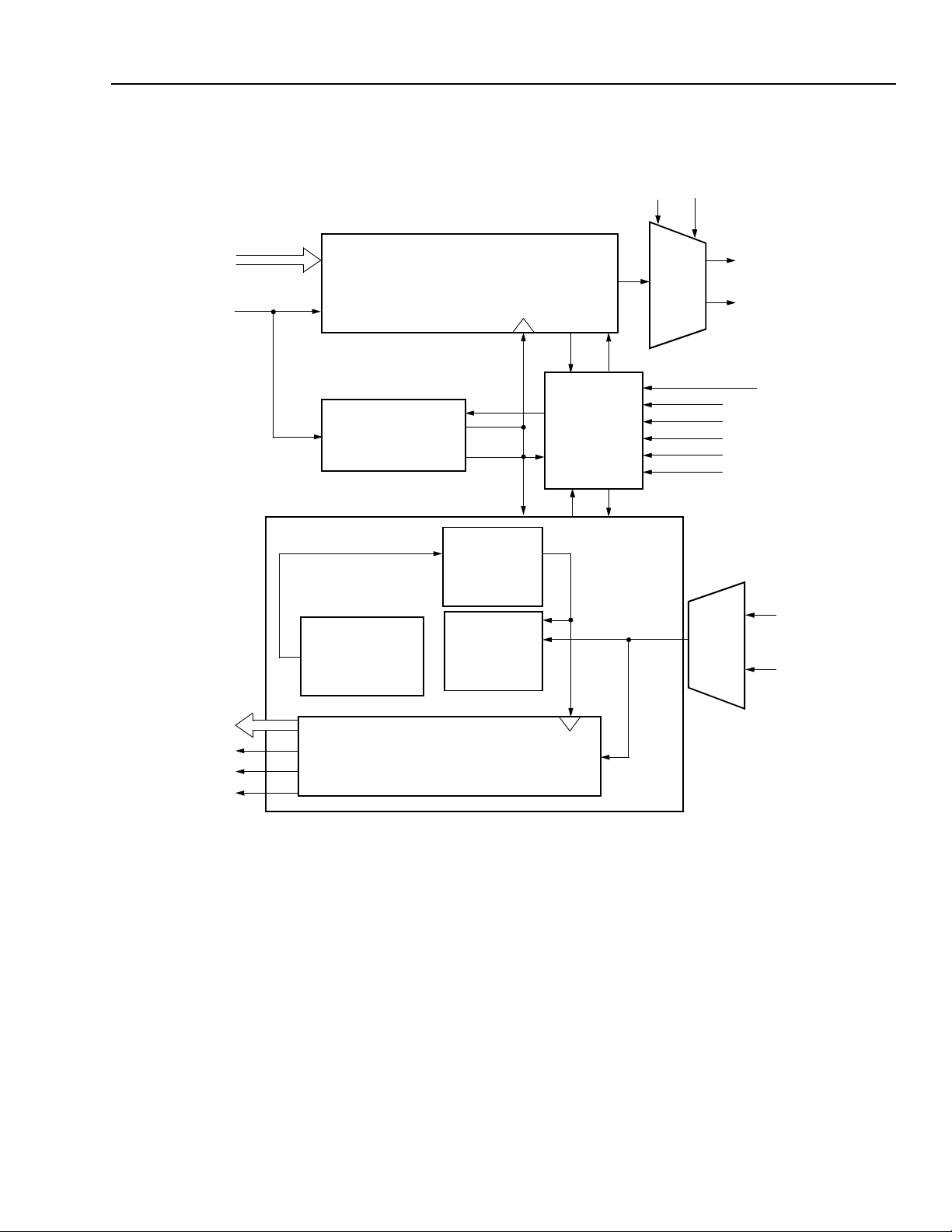
Functional Description
Block Diagrams
TX[9:0]
REFCLK
(continued)
DESERIALIZER
(continued)
DATA IN
LOAD
ANALOG PLL
SERIALIZER
PHASE SELECT/
INTERPOLATION
SERIAL DATA
OUT
GLOBAL
CONTROL
OLRVS
OLREF
PECL
TEST[5:1] / LDST
BYPPLL
RESETN
LPWR
ENCDET
EWRAP
HDOUTP
HDOUTN
RX[9:0]
RXCLK0
RXCLK1
COMDET
DIGITAL
LOW-PASS FILTER
DATA RETIMING, SERIAL-TO-PARALLEL
CONVERSION AND COMMA DETECTION
PHASE
DETECTOR
SERIAL
DATA
IN
PECL
Figure 2. LU5X34F Single-Channel Transceiver Functional Diagram
HDINP
HDINN
5-8809(F).a
.
Lucent Technologies Inc.
7
LU5X34F Preliminary Data Sheet
Quad Gigabit Ethernet Transceiver July 2000
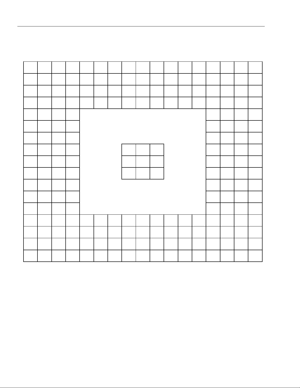
Input/Output Information
A UTRPNMLKJHGFEDCB
1
3
RXCLK0B RXB 9 VSS RXB4
RXB6 RXB2 EWRAPA
RXB7
RXB82
VSS RXB5 RXB1
LCKREFA LCKREFB TEST2 TEST4
ENCDETA EWRAPB RESETN TEST3
N/C LDSTA ENCDETB TEST1
BYPPLL REFCLK ENCDETC ENCDETD
TEST5 REFCLKN LDSTC LDSTD
LPWR EWRAPC LPBKD N/C
LCKREFD TXC1 TXC5 TXC5
TXC0 TXC4 TXC8 VSS
TXC3 TXC7 VSS N/C
N/C
TXCLKC
N/C
4
TXB9 RXCLK1B COMDETB VSS
5
TXB6 TXB8 N/C VDD
6
TXB4 TXB5 TXB7 TXCLKB
7
TXB0 TXB1 TXB3 TXB2
8
RXA1 RXA0 N/C VDD
9
RXA3 RXA4 RXA2 VSS
RXA5 RXA6 RXA8 VDD
0
RXA7 RXA9 RXCLK0A N/C
1
COMDETA RXCLK1A TXCLKA TXA7
2
N/C VDD TXA8 TXA4
3
TXA6 TXA3 VSST HDINAN
TXA9
4
TXA2 VSST HDINAP HDOUTAN
TXA5
5
VSST VSSRA VDDTA VSSRB
TXA1
6
RXB3 RXB0 LDSTB VDD
VSS VSS VSS
VSS VSS VSS
VSS VSS VSS
HDOUTAP HDOUTBP VDDR VSST
HDINBP HDOUTBN VSSP VREG
VSSRB VDDTB VDDP N/C
VSS VDD LCKREFC TXC2
VDDR VSSRC N/C VDDTD
VSSRC VDDTC HDOUTCP HDINDP
OLREF HDINCP HDOUTCN VDDTC
TXC6 VSS RXCLK1C COMDETC
RXCLK0C RXC8 RXC6 RXC4
RXC9 RXC5 RXC3 RXC0
RXC1 RXC2 N/C TXD1
VDD TXD0 TXD2 TXD3
VSS TXD6 TXD4 TXD5
VDD TXD10 TXD8 TXD7
N/C RXCLK1D TXCLKD N/C
RXD6 RXD9 N/C RXCLK0D
RXD2 RXD5 RXD8 COMDETD
VSS RXD1 RXD4 RXD7
HDOUTDN VSS RXD0 RXD3
HDINDN HDOUTDP VSS N/C
RXC7
TXA0 VSSRD VSSRD VDDTD N/C
7
N/C VSSRA VDDTA HDINBN
VDDTB VDDP VSSP N/C
OLRVS N/C HDINCN N/C
Figure 3. Pin Designations (Top View)
8
Lucent Technologies Inc.
5-8880(F)
 Loading...