

AGERE LU3X54FT-S208, LU3X54FT-HS208 Datasheet

LU3X54FT
QUAD-FET (Fast Ethernet Transceiver) for 10Base-T/100Base-TX/
FX
Data Sheet
July 2000
Introduction
The LU3X54FT is a four-channel, single-chip complete transceiver designed specifically for dual-speed
10Base-T, 100Base-TX, and 100Base-FX repeaters
and switches. It supports simultaneous operation in
three separate
IEEE
standard modes: 10Base-T,
100Base-TX, and 100Base-FX.
Each channel implements:
■
10Base-T transceiver function of
IEEE
802.3.
■
Physical coding sublayer (PCS) of
IEEE
802.3u.
■
Physical medium attachment (PMA) of
IEEE
802.3u.
■
Autonegotiation of
IEEE
802.3u.
■
MII management of
IEEE
802.3u.
■
Physical medium dependent (PMD) of
IEEE
802.3.
The LU3X54FT supports operations over two pairs of
unshielded twisted-pair (UTP) cable (10Base-T and
100Base-TX), and over fiber-optic cable (100BaseFX).
It has been designed with a flexible system interface
that allows configuration for optimum performance
and effortless design. The individual per-port interface can be configured as 100 Mbits/s MII, 10 Mbits/s
MII, 7-pin 10 Mbits/s serial, or bused mode.
Features
10 Mbits/s Transceiver
■
Compatible with
IEEE
* 802.3 10Base-T standard
for twisted-pair cable
■
Autopolarity detection and correction
■
Adjustable squelch level for extended line length
capability (two levels)
■
Interfaces with
IEEE
802.3u media independent
interface (MII) or a serial 10 Mbits/s 7-pin interface
■
On-chip filtering eliminates the need for external
filters
■
Half- and full-duplex operations
100 Mbits/s TX T r ansceiver
■
Compatib le wit h
IEEE
802.3u MII (clause 22), PCS
(clause 23), PMA (clause 24), autonegotiation
(clause 28), and PMD (clause 25) specifications
■
Scrambler/descrambler bypass
■
Encoder/decoder bypass
■
3-statable MII in 100 Mbits/s mode
■
Selectable carrier sense signal generation (CRS)
asserted during either transmission or reception in
half duplex (CRS asserted during reception only in
full duplex)
■
Selectable MII or 5-bit code group interface
■
Full- or half-duplex operations
■
Optional carrier integrity monitor (CIM)
■
On-chip filtering and adaptive equalization that
eliminates the need for external filters
*
IEEE
is a registered trademark of The Institute of Electrical and Electronics Engineers, Inc.
Note: Advisories are issued as needed to update product information. When using this data sheet for design purposes, please contact
your Lucent Technologies Microelectronics Group Account Manager to obtain the latest advisory on this product.

Table of Contents
Contents Page
LU3X54FT Data Sheet
QUAD-FET for 10Base-T/100Base-TX/FX July 2000
2 Lucent Technologies Inc.
Introduction ........................ ....................................... ...................................... ................................. .........................1
Features ...................................................................................................................................................................1
10 Mbits/s Transceiver........................................................................................................................................... 1
100 Mbits/s TX Transceiver ................................................................................................................................... 1
100 Mbits/s FX Transceiver ................................................................................................................................... 4
General .................................................................................................................................................................. 4
Description ...............................................................................................................................................................4
Bused MII Mode..................................................................................................................................................... 4
Clocking ................................................................................................................................................................. 5
FX Mode ................................................................................................................................................................ 6
Functional Block Diagrams .................................................................................................................................... 7
Application Diagrams. ...... ...... ....... ...... ....... ...... ....... ...... ....................................... ...... ....... ...... ....... ...... ....... ...... ..... 9
Block Diagrams.................................................................................................................................................... 11
Pin Information .......................................................................................................................................................13
Pin Diagram for Normal MII Mode ....................................................................................................................... 13
Pin Diagram for Bused MII Mode......................................................................................................................... 14
Pin Maps.......................... ...... ....... ...... ....... ...... ....... ...... ....... ...... ....... ................................................................ ... 15
Pin Descriptions..................... ....... ...... ....... ....................................... ...... ...... ....... ...... ...... . ...... ....... ...... ................ 16
MII Station Management .......................................... ...................................... ....... ...... ....... ...... ....... ...... ....... ...... ....29
Basic Operations.................................................................................................................................................. 29
MII Management Frames..................................................................................................................................... 29
Management Registers (MR)............................................................................................................................... 30
Unmanaged Operations....................................................................................................................................... 40
Mode Select..................... ...... ....... ...... ....... ...... ....... ...... ....... ...................................... ....... ...... ....... ...... ....... ...... ... 40
Absolute Maximum Ratings (TA = 25 °C) ............................................................................................................... 41
Electrical Characteristics ........................................................................................................................................41
Package and Thermal Characteristics ....................................................................................................................42
Outline Diagram ......................................................................................................................................................52
208-Pin SQFP...................................................................................................................................................... 52
Tables Page
Table 1. LU3X54FT Crystal Specifications .............................................................................................................. 6
Table 2 . LU3X54FT Pin Maps............................................................................................................................... 15
Table 3. MII/Serial Interface Pins in Normal MII Mode (Four Separate MII Ports)................................................. 16
Table 4. MII/Serial Interface Pins in Bused MII Mode............................................................................................ 18
Table 5. MII Management Pins .............................................................................................................................. 22
Table 6. 10/100 Mbits/s Twisted-Pair (TP) Interface Pins....................................................................................... 22
Table 7. Miscellaneous Pins .................................................................................................................................. 23
Table 8. MII Management Frame Format............................................................................................................... 29
Table 9. MII Management Frames Field Descriptions............................................................................................ 29
Table 10. MII Management Registers (MR)........................................................................................................... 30
Table 11. MR0—Control Register Bit Descriptions................................................................................................ 31
Table 12. MR1—Status Register Bit Descriptions ................................................................................................. 32
Table 13. MR2, 3—PHY Identifier Registers (1 and 2) Bit Descriptions................................................................ 33
Table 14. MR4—Autonegotiation Advertisement Register Bit Descriptions........................................................... 33
Table 15. MR5—Autonegotiation Link Partner (LP) Ability Register (Base Page) Bit Descriptions ....................... 34
Table 16. MR5—Autonegotiation Link Partner (LP) Ability Register (Next Page) Bit Descriptions........................ 34
Table 17. MR6—Autonegotiation Expansion Register Bit Descriptions................................................................. 35
Table 18. MR7—Next-Page Transmit Register Bit Descriptions ............................................................................ 35

Lucent Technologies Inc. 3
Data Sheet LU3X54FT
July 2000 QUAD-FET for 10Base-T/100Base-TX/FX
Table of Contents
Tables Page
Table 19. MR28—Device-Specific Register 1 (Status Register) Bit Descriptions...................................................36
Table 20. MR29—Device-Specific Register 2 (100 Mbits/s Control) Bit Descriptions............................................37
Table 21. MR30—Device-Specific Register 3 (10 Mbits/s Control) Bit Descriptions..............................................38
Table 22. MR31—Device-Specific Register 4 (Quick Status) Bit Descriptions.......................................................39
Table 23. Output Pins.............................................................................................................................................40
Table 24. LU3X54FT Modes...................................................................................................................................40
Table 25 . Absolute Maximum Ratings ...................................................................................................................41
Table 26 . Operating Conditions.............................................................................................................................41
Table 27. dc Characteristics ...................................................................................................................................41
Table 28. Thermal Characteristics..........................................................................................................................42
Table 29. MII Management Interface Timing (25 pF Load).....................................................................................43
Table 30. MII Data Timing (25 pF Load).................................................................................................................44
Table 31. Serial 10 Mbits/s Timing for TPIN, CRS, and RX_CLK...........................................................................46
Table 32. Serial 10 Mbits/s Timing for TX_EN, TPOUT, CRS, and RX_CLK..........................................................46
Table 33. Serial 10 Mbits/s Timing for TX_EN, TPIN, and COL.............................................................................47
Table 34. Serial 10 Mbits/s Timing for RX_CLK, CRS, RXD, TX_CLK, TX_EN, and TXD (25 pF Load)................48
Table 35. Serial 10 Mbits/s Timing for RX_CLK and TX_CLK (25 pF Load) ..........................................................49
Table 36. 100 Mbits/s MII Transmit Timing .............................................................................................................50
Table 37. 100 Mbits/s MII Receive Timing..............................................................................................................51
Figures Page
Figure 1. LU3X54FT Device Overview.....................................................................................................................7
Figure 2. LU3X54FT Single-Channel Detail Functions ............................................................................................8
Figure 3. Typical Single-Channel Twisted-Pair (TP) Interface..................................................................................9
Figure 4. Typical Single-Channel Fiber-Optic Interface..........................................................................................10
Figure 5. Smart 10/100 Mbits/s Bused MII Mode...................................................................................................11
Figure 6. Separate 10/100 Mbits/s Bused MII Mode..............................................................................................12
Figure 7. LU3X54FT Pinout for Normal MII Mode..................................................................................................13
Figure 8. LU3X54FT Pinout for Bused MII Mode...................................................................................................14
Figure 9. Thermal Characteristics..........................................................................................................................42
Figure 10. MDIO Input Timing................................................................................................................................43
Figure 11. MDIO Output Timing.............................................................................................................................43
Figure 12. MDIO During TA (Turnaround) of a Read Transaction ..........................................................................43
Figure 13. MII Timing Requirements for LU3X54FT ..............................................................................................45
Figure 14. Serial 10 Mbits/s Timing for TPIN, CRS, and RX_CLK.........................................................................46
Figure 15. Serial 10 Mbits/s Timing for TX_EN, TPOUT, CRS, and RX_CLK........................................................46
Figure 16. Serial 10 Mbits/s Timing for TX_EN, TPIN, and COL ...........................................................................47
Figure 17. Serial 10 Mbits/s Timing for RX_CLK, CRS, RXD, TX_CLK, TX_EN, and TXD ...................................48
Figure 18. Serial 10 Mbits/s Timing Diagram for RX_CLK and TX_CLK ...............................................................49
Figure 19. 100 Mbits/s MII Transmit Timing ...........................................................................................................50
Figure 20. 100 Mbits/s MII Receive Timing............................................................................................................51
(continued)

4 Lucent Technologies Inc.
LU3X54FT Data Sheet
QUAD-FET for 10Base-T/100Base-TX/FX July 2000
Features
(continued)
100 Mbits/s FX Transceiver
■
Compatible with
IEEE
802.3U 100Base-FX standard
■
Reuses existing twisted-pair I/O pins for compatible
fiber-optic transceiver pseudo-ECL (PECL) data:
— No additional data pins required
— Reuses existing LU3X54FT pins for fiber-optic sig-
nal detect (FOSD) inputs
■
Fiber mode automatically configures port:
— Disables autonegotiation
— Disables 10Base-T
— Enables 100Base-FX remote fault signaling
— Disables MLT-3 encoder/decoder
— Disables scrambler/descrambler
■
FX mode enable is pin- or register-selectable on an
individual per-port basis.
General
■
Autonegotiation (
IEEE
802.3u, clause 28):
— Fast link pulse (FLP) burst generator
— Arbitration function
■
Bused interfaces:
— Supports either separate 10 Mbits/s and
100 Mbits/s multiport repeaters (100 Mbits/s
MII and 10 Mbits/s serial data stream), or singlechip multispeed repeaters
— Connects ports to either the 10 Mbits/s or
100 Mbits/s buses controlled by autonegotiation
— Separate TX_EN, RX_EN, CRS, and COL pins for
each port
— Drivers on bused signal can drive up to eight
LU3X54FTs (32 ports)
■
Supports the station management protocol and
frame format (clause 22):
— Basic and extended registers
— Supports next-page function
— Operates up to 12.5 MHz
— Accepts preamble suppression
— Maskable status interrupts
■
Supports the following management functions via
pins if MII station management is unavailable:
— Speed select
— Carrier integrity enable
— Encoder/decoder bypass
— Scrambler/descrambler bypass
— Full duplex
— No link pulse mode
— Carrier sense select
— Autonegotiation
— 10 Mbits/s repeater reference select
— Internal 20 MHz clock synthesizer
— FX mode select
■
Single 25 MHz crystal input or 25 MHz clock input,
optional 20 MHz clock input
■
Supports half- and full-duplex operations
■
Provides six status signals:
— Receive activity
— Transmit activity
— Full duplex
— Collision/jabber
— Link integrity
— Speed indication
■
Optional LED pulse stretching
■
Per-channel powerdown mode for 10 Mbits/s and
100 Mbits/s operation
■
Loopback for 10 Mbits/s and 100 Mbits/s operation
■
Internal pull-up or pull-down resistors to set default
powerup mode
■
0.35 µm, low-power CMOS technology
■
208-pin SQFP or 208-pin SQFPH
■
Single 5 V power supply
Description
Bused MII Mode
The LU3X54FT has been designed for operation in two
basic system interface modes of operation:
■
Normal MII Mode (Four Separate MII Ports).
The
separate mode provides four independent RJ-45 to
MII ports and is similar to having four independent
10/100 transceivers.
■
Bused MII Mode.
This mode is designed specifically
for repeater applications to save pins. In bused
mode:
— Data from all of the ports operating at 100 Mbits/s
will be internally bused to system interface port A
(100 Mbits/s MII interface).
— Data from all of the ports operating at 10 Mbits/s
will be internally bused to system interface port B
(7-pin 10 Mbits/s serial interface).
The LU3X54FT will automatically detect the speed of
each port (10 Mbits/s or 100 Mbits/s) and route the
data to the appropriate port.

Lucent Technologies Inc. 5
Data Sheet LU3X54FT
July 2000 QUAD-FET for 10Base-T/100Base-TX/FX
Description
(continued)
Bused MII Mode
(continued)
The bused mode has two additional submodes of
operation:
■
Separate Bused MII Mode.
This mode is designed
to operate with two independent repeater ICs, one
repeater operating at 100 Mbits/s and the other operating at 10 Mbits/s.
Figure 6 shows a block diagram of this mode in which
separate pins (four of each) are used for COL_10(4),
COL_100(4), CRS_10(4), CRS_100(4),
RX_EN10(4), RX_EN100(4), TX_EN10 (4), and
TX_EN100(4).
The signals RX_CLK10, RXD_10, TX_CLK10, and
TXD_10 (all from ports A, B, C, and D) are internally
bused together and connected to MII port B.
The signals TX_CLK25, TXD_100[3:0], TX_ER,
RX_CLK25, RXD_100[3:0], RX_DV, and RX_ER (all
from ports A, B, C, D) are internally bused together
and connected to MII port A.
The repeater ICs will enable the particular port to
which it will communicate by enabling the port with
TX_EN 10, TX_EN100, RX_EN10, or RX_EN100.
■
Smart Bused MII Mode.
This mode is used when
the LU3X54FT is communicating with a single
(smart) 10/100 Mbits/s repeater IC, and allows the
use of the security feature.
Figure 5 shows a block diagram of the smart bused
mode of operation. In this mode, a common set of
pins is used for CRS10/100, RX_EN10/100,
TX_EN10/100, and COL_10/100.
The 10 Mbits/s (7-pin 10 Mbits/s serial interface) signals are still routed to port B (RX_CLK10, RXD_10,
TX_CLK10, and TXD_10).
The 100 Mbits/s signals are still routed to port A
(TX_CLK25, TXD_100[3:0], TX_ER, RX_CLK25,
RXD_100[3:0], RX_DV, and RX_ER).
The bused interface allows each of the four transceivers to be connected to one of two system interfaces:
■
Port A: 100 Mbits/s MII interface.
■
Port B: 7-pin 10 Mbits/s serial interface.
This configuration allows 10/100 Mbits/s segment segregation or port switching with conventional multiport
shared-media repeaters.
The port speed configuration and connection to the
appropriate bused output is done automatically and is
controlled by autonegotiation.
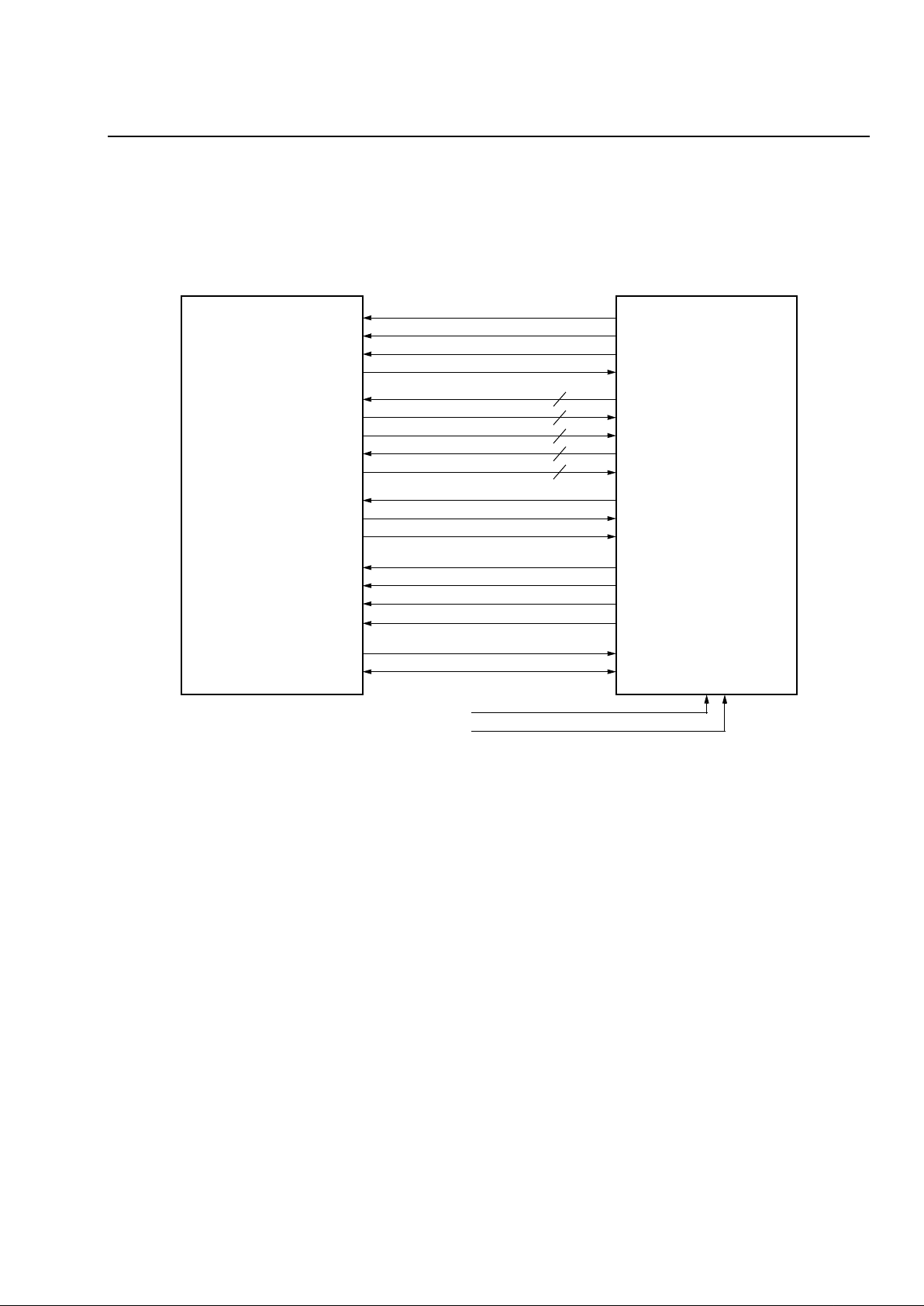
Figure 1 gives a functional overview of the LU3X54FT
while Figure 2 details its single-channel functions.
Figure 3 shows how the LU3X54FT single channel
interfaces to the twisted pair (TP).
Clocking
The LU3X54FT requires an internal 25 MHz clock and
a 20 MHz clock to run the 100Base-TX transceiver and
10Base-T transceiver.
These clocks can be supplied as follows:
■
As separate clock inputs: 25 MHz and 20 MHz.
■
The 20 MHz clock can be internally synthesized from
the 25 MHz clock.
■
The 25 MHz clock can also be internally generated
by an on-chip oscillator if an external crystal is supplied.
The LU3X54FT will automatically detect if a 25 MHz
clock is supplied, or if a crystal is being used to generate the 25 MHz clock.

6 Lucent Technologies Inc.
LU3X54FT Data Sheet
QUAD-FET for 10Base-T/100Base-TX/FX July 2000
Description
(continued)
Clocking
(continued)
Either the on-chip 20 MHz clock synthesizer (default
clock) can be used, or H-DUPLED[A]/CLK20_SEL
(pin 198) can be pulled high (sensed on powerup and
reset) to select the external 20 MHz clock input.
The crystal specifications for the device are listed in
Table 1, and the crystal circuit is sh o wn in Fi gure 3 an d
Figure 4.
Table 1. LU3X54FT Crystal Specifications
FX Mode
Each individual port of the LU3X54FT can be operated
in 100Base-FX mode by selecting it through the pin
program option (RXLED[D:A]/FX_MODE_EN[D:A], or
through the register bit (register 29, bit 0). FX mode
can operate in full or half duplex. Each individual channel’s duplex can be set by register zero bit eight (0.8) or
all ports duplex can be hardware configured at power
up or rest by pin 201 FULL_DUP.
When operating in FX mode, the twisted-pair I/O pins
are reused as the fiber-optic transceiver I/O data pins,
and the fiber-optic signal detect (FOSD) inputs are
enabled.
Figure 4 shows a typical FX port interface. Note that no
additional external components, excluding those
needed by the fiber transceiver, are required.
When a port is placed in FX mode, it will automatically
configure the port for 100Base-FX operation (and the
register bit control will be ignored) such that:
■
The far-end fault signaling option will be enabled.
■
The MLT-3 encoding/decoding will be disabled.
■
Scrambler/descrambler will be disabled.
■
Autonegotiation will be disabled.
■
The signal detect inputs will be activated.
■
10Base-T will be disabled.
Parameter Requirement
Type Quartz Fundamental Mode
Frequency 25 MHz
Stability ±25 ppm, 0 °C—70 °C
Shunt Capacitor 7 pF
Load Capacitor 20 pF
Series Resistance <30
Ω
Lucent Technologies Inc. 7
Data Sheet LU3X54FT
July 2000 QUAD-FET for 10Base-T/100Base-TX/FX
Description
(continued)
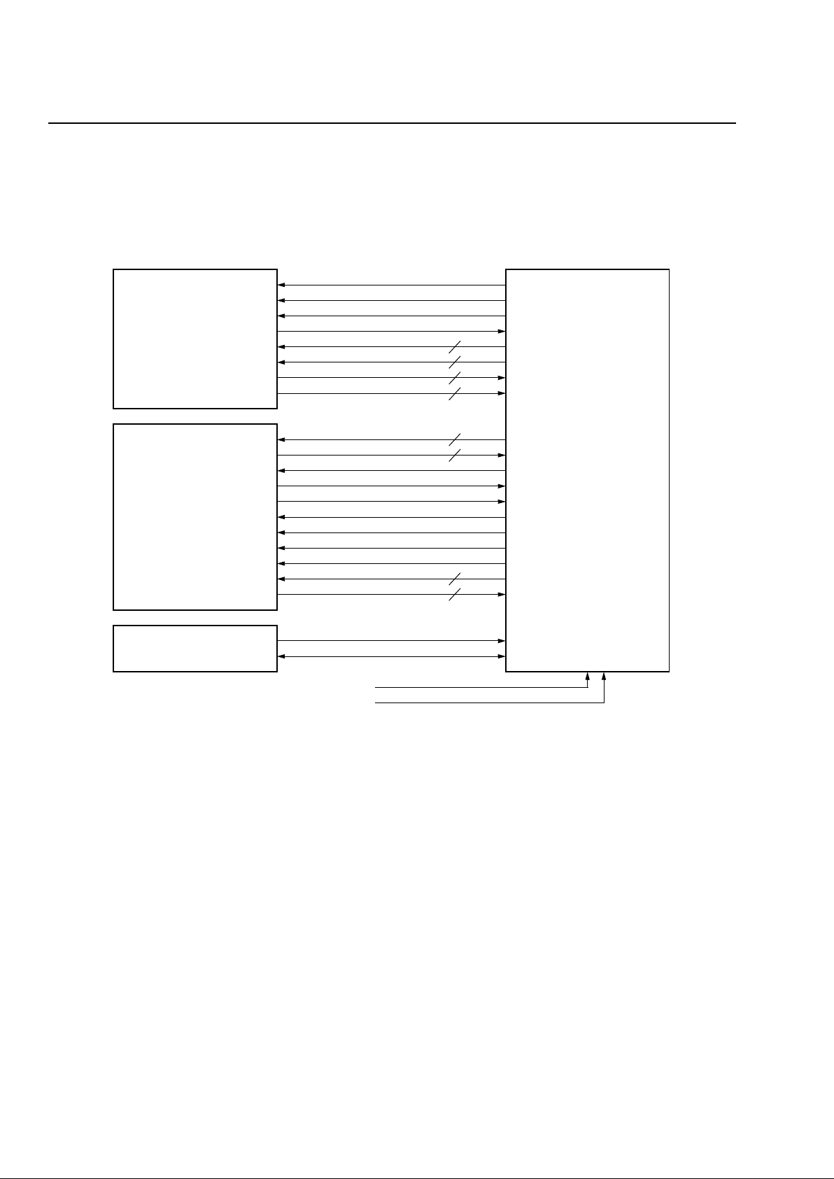
Functional Block Diagrams
Device Overview
5-5137(F).fr2
Figure 1. LU3X54FT Device Overview
10 Mbits/s TRANSCEIVER
AUTONEGOTIATION
PMA
PMA
PMA
PMA
TX PMD/
MUX
MANAGEMENT
PCS
MANAGEMENT
PCS
MANAGEMENT
PCS
MANAGEMENT
PCS
MII/SERIAL
AUTONEGOTIATION
AUTONEGOTIATION
AUTONEGOTIATION
MUX
MUX
MUX
DPLL
10 MHz
25 MHz
125 MHz
LSCLK
INTERFACE
MII/SERIAL
INTERFACE
MII/SERIAL
INTERFACE
MII/SERIAL
INTERFACE
20 MHz
25 MHz
DRIVER AND FILTERS
10 Mbits/s TRANSCEIVER
DRIVER AND FILTERS
10 Mbits/s TRANSCEIVER
DRIVER AND FILTERS
10 Mbits/s TRANSCEIVER
DRIVER AND FILTERS
DRIVER AND
FILTERS
DRIVER AND
FILTERS
DRIVER AND
FILTERS
DRIVER AND
FILTERS
TP
MAGNETICS
INTERFACE
20 MHz
25 MHz
CRYSTAL
FX PORT
FX_MODE_EN
TX PMD/
FX PORT
TX PMD/
FX PORT
TX PMD/
FX PORT
FX_MODE_EN
FX_MODE_EN
FX_MODE_EN
LU3X54FT Data Sheet
QUAD-FET for 10Base-T/100Base-TX/FX July 2000
8 Lucent Technologies Inc.
Description
(continued)
Functional Block Diagrams
(continued)
Single-Channel Detail Functions
5-5136(F).gr4
Figure 2. LU3X54FT Single-Channel Detail Functions
AUTONEGOTIATION
AND LINK MONITOR
100 OFF
TXD[3:0]
4B/5B
ENCODER
FAR-END
FAULT GEN
SCRAMBLER
PDT
DCRU
SD
PDR
DESCRAMBLER
ALIGNER
5B/4B
DECODER
FAR-END
FAULT DETECT
10 Mbits/s TRANSCEIVER
RX_CLK
RXD[0]
TX_CLK
TX_EN
TXD[0]
CLK20
MDC
MDIO
MII
TPIN
±
TX STATE
MACHINE
SD
COLLISION
DETECT
SD
RX STATE
MACHINE
MII
TX_ER/TXD[4]
TX_EN
TXD[3:0]
TX_CLK
RX_CLK
RX_ER/RXD[4]
RX_DV
RXD[3:0]
COL
CRS
REF10
MANAGEMENT
25 MHz
125 MHz
LSCLK
PMD
TX/
PMD
RX/
SD
TPOUT
±
100 Mbits/s TRANSCEIVER
LC10 LS10
LC100
LS100
CARRIER
CIM
DETECT
RXERR_ST
CAR_STAT
MII
INTERFACE
SERIAL
INTERFACE
DPLL
25 MH
Z
MANAGEMENT
INTERFACE
20 MHz
25 MHz
CRYSTAL
FIBER PORT
FX_MODE_EN
FX_MODE_EN
FIBER
PORT
FOSD
Lucent Technologies Inc. 9
Data Sheet LU3X54FT
July 2000 QUAD-FET for 10Base-T/100Base-TX/FX
Description
(continued)
Application Diagrams
Single-Channel Twisted-Pair Interface
5-5433(F).r9
Figure 3. Typical Single-Channel Twisted-Pair (TP) Interface
LU3X54FT
RJ-45
1
2
3
4
5
6
7
8
75
Ω
75
Ω
0.01 µF
1:1
1:1
0.01 µF
0.01 µF
0.01 µF
220
Ω
TPIN+
TPIN–
TPOUT+
TPOUT–
220
Ω
50
Ω
50
Ω
V
DDO
75
Ω
0.01 µF
75
Ω
XTALOUT
XTALIN
88 87
33 pF 33 pF
25 MHz
50
Ω
50
Ω
0.01 µF
LU3X54FT Data Sheet
QUAD-FET for 10Base-T/100Base-TX/FX July 2000
10 Lucent Technologies Inc.
Description
(continued)
Application Diagrams
(continued)
Single-Channel Fiber-Optic Interface
5-5433(F).dr2
Figure 4. Ty pical Single-Channel Fiber-Optic Interface
LU3X54FT
TD
TDN
SD
RD
RDN
0.01 µF
220
Ω
TPIN+
TPIN–
TPOUT+
TPOUT–
220
Ω
50
Ω
50
Ω
V
DDO
82
Ω
0.01 µF
130
Ω
XTALOUT
XTALIN
88 87
33 pF 33 pF
25 MHz
FOSD
50
Ω
50
Ω
82
Ω
130
Ω
82
Ω
130
Ω
V
DDA
0.01 µF
Lucent Technologies Inc. 11
Data Sheet LU3X54FT
July 2000 QUAD-FET for 10Base-T/100Base-TX/FX
Description
(continued)
Block Diagrams
Smart Bused MII Mode
5-5599.br2
Figure 5. Smart 10/100 Mbits/s Bused MII Mode
RX_CLK10
RXD_10
TX_CLK10
TXD_10
COL_100
CRS_100
RX_EN100
TX_EN100
TX_EN10/SECURITY
TX_CLK25
TXD_100[3:0]
TX_ER
RX_CLK25
RXD_100[3:0]
RX_DV
RX_ER
MDC
MDIO
SMART_MODE_SELECT
BUSED_MII_MODE
LU3X54FT
10/100 Mbits/s
REPEATER
RX_CLK10
RXD_10
TX_CLK10
TXD_10
COL_10/100
CRS_10/100
RX_EN10/100
TX_EN10/100
SECURITY10/100
TX_CLK25
TXD_100[3:0]
TX_ER
RX_CLK25
RXD_100[3:0]
RX_DV
RX_ER
MDC
MDIO
SMART
4
4
4
4
4
LU3X54FT Data Sheet
QUAD-FET for 10Base-T/100Base-TX/FX July 2000
12 Lucent Technologies Inc.
Description
(continued)
Block Diagrams
(continued)
Separate Bused MII Mode
5-5599.ar5
Figure 6. Separate 10/100 Mbits/s Bused MII Mode
RX_CLK10
RXD_10
TX_CLK10
TXD_10
COL_10
CRS_10
RX_EN10
TX_EN10
CRS_100
TX_EN100
TX_CLK25
TXD_100[3:0]
TX_ER
RX_CLK25
RXD_100[3:0]
RX_DV
RX_ER
COL_100
RX_EN100
MDC
MDIO
SMART_MODE_SELECT
BUSED_MII_MODE
LU3X54FT
10 Mbits/s
REPEATER
100 Mbits/s
REPEATER
MANAGEMENT
RX_CLK10
RXD_10
TX_CLK10
TXD_10
COL_10
CRS_10
RX_EN10
TX_EN10
CRS_100
TX_EN100
TX_CLK25
TXD_100[3:0]
TX_ER
RX_CLK25
RXD_100[3:0]
RX_DV
RX_ER
COL_100
RX_EN100
MDC
MDIO
4
4
4
4
4
4
4
4
Lucent Technologies Inc. 13
Data Sheet LU3X54FT
July 2000 QUAD-FET for 10Base-T/100Base-TX/FX
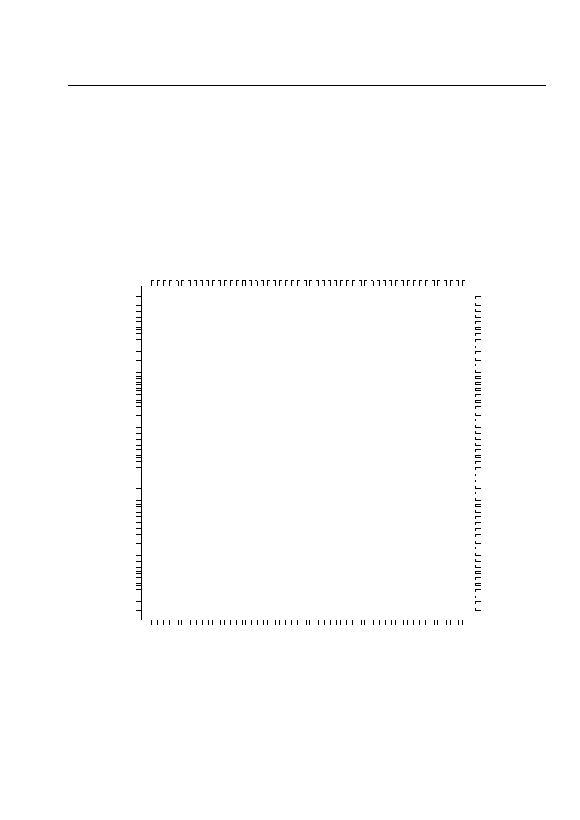
Pin Information
Pin Diagram for Normal MII Mode
5-5616(F).ar4
Figure 7. LU3X54FT Pinout for Normal MII Mode
VSS
156
RXD[0][B]
155
RX_CLK[B]
154
RX_ER[B]/RXD[4][B]
153
VDD
152
RX_DV[B]
151
COL[B]
150
CRS[B]
149
TX_CLK[B]
148
VSS
147
TX_EN[B]
146
TX_ER[B]/TXD[4][B]
145
VDD
144
TXD[3][B]
143
TXD[2][B]
142
VSS
141
TXD[1][B]
140
TXD[0][B]
139
MII_EN[A]
138
VDD
137
RXD[3][A]
136
RXD[2][A]
135
RXD[1][A]
134
VSS
133
RXD[0][A]
132
RX_CLK[A]
131
RX_ER[A]/RXD[4][A]
130
VDD
129
RX_DV[A]
128
COL[A]
127
CRS[A]
126
TX_CLK[A]
125
VSS
124
TX_EN[A]
123
TX_ER[A]/TXD[4][A]
122
VDD
121
TXD[3][A]
120
TXD[2][A]
119
VSS
118
TXD[1][A]
117
TXD[0][A]
116
VSS
115
REF10
114
MDC
113
MDIO
112
VDD
111
MII_EN[D]
110
RXD[3][D]
109
RXD[2][D]
108
RXD[1][D]
107
VSS
106
RXD[0][D]
105
GNDA
1
FOSD[C]
2
FOSD[D]
3
VDDA
4
TPIN+/FOIN+[D]
5
TPIN–/FOIN–[D]
6
GNDA
7
VDDA
8
TPIN+/FOIN+[C]
9
TPIN–/FOIN–[C]
10
GNDA
11
VDDA
12
BGREF0
13
GNDA
14
VDDA
15
TPIN+/FOIN+[B]
16
TPIN–/FOIN–[B]
17
GNDA
18
VDDA
19
TPIN+/FOIN+[A]
20
TPIN–/FOIN–[A]
21
GNDA
22
VDDA
23
GNDA
24
BGREF1
25
GNDD
26
CLK20
27
VDDD
28
GNDAA
29
VDDAA
30
GNDO
31
TPOUT+/FOOUT+[D]
32
TPOUT–/FOOUT–[D]
33
VDDO
34
GNDO
35
TPOUT+/FOOUT+[C]
36
TPOUT–/FOOUT–[C]
37
VDDO
38
GNDM
39
VDDM
40
GNDAP
41
ISET_10
42
ISET_100
43
VDDAP
44
GNDO
45
TPOUT+/FOOUT+[B]
46
TPOUT–/FOOUT–[B]
47
VDDO
48
GNDO
49
TPOUT+/FOOUT+[A]
50
TPOUT–/FOOUT–[A]
51
VDDO
52
RX_CLK[D]
104
RX_ER[D]/RXD[4][D]
103
VDD
102
RX_DV[D]
101
COL[D]
100
CRS[D]
99
TX_CLK[D]
98
VSS
97
TX_EN[D]
96
TX_ER[D]TXD[4][D]
95
VDD
94
TXD[3][D]93TXD[2][D]
92
VSS
91
TXD[1][D]90TXD[0][D]
89
XTALOUT
88
LSCLK/XTALIN
87
VSSPD
86
FOSD[B]85FOSD[A]
84
VDDPD
83
VSSPLL
82
CKREF
81
VDDPLL
80
VSS
79
MII_EN[C]
78
VDD
77
RXD[3][C]76RXD[2][C]75RXD[1][C]
74
VSS
73
RXD[0][C]
72
RX_CLK[C]
71
RX_ER[C]/RXD[4][C]
70
VDD
69
RX_DV[C]
68
COL[C]
67
CRS[C]
66
TX_CLK[C]
65
VSS
64
TX_EN[C]
63
TX_ER[C]/TXD[4][C]
62
VDD
61
TXD[3][C]60TXD[2][C]
59
VSS
58
TXD[1][C]57TXD[0][C]
56
MODE[4]
55NC54
MASK_STAT_INT
53
RXD[1][B]
157
RXD[2][B]
158
RXD[3][B]
159
VDD
160
MII_EN[B]
161
TXLED[A]/REF_SEL
162
VSS
163
TXLED[B]/SCRAM_DESC_BYPASS
164
TXLED[C]/ENC_DEC_BYPASS
165
TXLED[D]/CARIN_EN
166
VDD167
RXLED[A]/FX_MODE_EN[A]
168
RXLED[B]/FX_MODE_EN[B]
169
RXLED[C]/FX_MODE_EN[C]
170
RXLED[D]/FX_MODE_EN[D]
171
VDD
172
COLED[A]
173
COLED[B]
174
COLED[C]
175
COLED[D]
176
VSS
177
GNDC
178
VDDC
179
VDDC
180
GNDC
181
GNDA
182
ATEST[A]
183
ATEST[B]
184
VDDA
185
VSS
186
LINKLED[A]/NO_LP
187
LINKLED[B]/PHYADD[0]
188
LINKLED[C]/PHYADD[1]
189
LINKLED[D]/PHYADD[2]
190
SPEEDLED[A]/ISOLATE_MODE
191
SPEEDLED[B]/BUSED_MII_MODE
192
SPEEDLED[C]/SMART_MODE_SELECT
193
SPEEDLED[D]/SPEED
194
VDD
195
3ST_EN
196
AUTO_EN
197
H_DUPLED[A]/CLK20_SEL
198
H_DUPLED[B]/CRS_SEL
199
H_DUPLED[C]/SERIAL_SEL
200
H_DUPLED[D]/FULL_DUP
201
VDD
202
RESET
203
MODE[0]
204
MODE[1]
205
MODE[2]
206
MODE[3]
207
VSS
208
LU3X54FT

LU3X54FT Data Sheet
QUAD-FET for 10Base-T/100Base-TX/FX July 2000
14 Lucent Technologies Inc.
Pin Information
(continued)
Pin Diagram for Bused MII Mode
5-5616(F).br2
Figure 8. LU3X54FT Pinout for Bused MII Mode
VSS
156
RXD_10
155
RX_CLK10
154
NC
153
VDD
152
NC
151
COL_100[B]/COL_10/100[B]
150
CRS_100[B]/CRS_10/100[B]
149
TX_CLK10
148
VSS
147
TX_EN100[B]/TX_EN10/100
146
NC
145
VDD
144
NC
143
NC
142
VSS
141
NC
140
TXD_10
139
RX_EN100[A]/RX_EN10/100[
A
138
VDD
137
RXD_100[3]
136
RXD_100[2]
135
RXD_100[1]
134
VSS
133
RXD_100[0]
132
RX_CLK25
131
RX_ER
130
VDD
129
RX_DV
128
COL_100[A]/COL_10/100[A]
127
CRS_100[A]/CRS_10/100[A]
126
TX_CLK25
125
VSS
124
TX_EN100[A]/TX_EN10/100
123
TX_ER
122
VDD
121
TXD_100[3]
120
TXD_100[2]
119
VSS
118
TXD_100[1]
117
TXD_100[0]
116
VSS
115
REF10
114
MDC
113
MDIO
112
VDD
111
RX_EN100[D]/RX_EN10/100[
D
110
CRS_10[D]
109
CRS_10[C]
108
CRS_10[B]
107
VSS
106
CRS_10[A]
105
GNDA
1
FOSD[C]
2
FOSD[D]
3
VDDA
4
TPIN+/FOIN+[D]
5
TPIN–/FOIN–[D]
6
GNDA
7
VDDA
8
TPIN+/FOIN+[C]
9
TPIN–/FOIN–[C]
10
GNDA
11
VDDA
12
BGREF0
13
GNDA
14
VDDA
15
TPIN+/FOIN+[B]
16
TPIN–/FOIN–[B]
17
GNDA
18
VDDA
19
TPIN+/FOIN+[A]
20
TPIN–/FOIN–[A]
21
GNDA
22
VDDA
23
GNDA
24
BGREF1
25
GNDD
26
CLK20
27
VDDD
28
GNDAA
29
VDDAA
30
GNDO
31
OUT+/FOOUT+[D]
32
POUT–/FOOUT–[D]
33
VDDO
34
GNDO
35
OUT+/FOOUT+[C]
36
POUT–/FOOUT–[C]
37
VDDO
38
GNDM
39
VDDM
40
GNDAP
41
ISET_10
42
ISET_100
43
VDDAP
44
GNDO
45
POUT+/FOOUT+[B]
46
POUT–/FOOUT–[B]
47
VDDO
48
GNDO
49
POUT+/FOOUT+[A]
50
POUT–/FOOUT–[A]
51
VDDO
52
NC
104NC103
VDD
102NC101
COL_100[D]/COL_10/100[D]
100
CRS_100[D]/CRS_10/100[D]
99NC98
VSS
97
TX_EN100[D]/TX_EN10/100
96NC95
VDD
94
TX_EN10[D]/SECURITY_10/10093TX_EN10[C]/SECURITY_10/100
92
VSS
91
TX_EN10[B]/SECURITY_10/10090TX_EN10[A]/SECURITY_10/100
89
XTALOUT
88
LSCLK/XTALIN
87
VSSPD
86
FOSD[B]85FOSD[A]
84
VDDPD
83
VSSPLL
82
CKREF
81
VDDPLL
80
VSS
79
RX_EN100[C]/RX_EN10/100[C]
78
VDD
77
COL_10[D]76COL_10[C]
75
COL_10[B]
74
VSS
73
COL_10[A]
72NC71NC70
VDD
69NC68
COL_100[C]/COL_10/100[C]
67
CRS_100[C]/CRS_10/100[C]
66NC65
VSS
64
TX_EN100[C]/TX_EN10/100
63NC62
VDD
61
RX_EN10[D]60RX_EN10[C]
59
VSS
58
RX_EN10[B]57RX_EN10[A]
56
MODE[4]
55NC54
MASK_STAT_INT
53
NC
157NC158NC159
VDD
160
RX_EN100[B]/RX_EN10/100[B]
161
TXLED[A]/REF_SEL
162
VSS
163
TXLED[B]/SCRAM_DESC_BYPASS
164
TXLED[C]/ENC_DEC_BYPASS
165
TXLED[D]/CARIN_EN
166
VDD167
RXLED[A]/FX_MODE_EN[A]
168
RXLED[B]/FX_MODE_EN[B]
169
RXLED[C]/FX_MODE_EN[C]
170
RXLED[D]/FX_MODE_EN[D]
171
VDD
172
COLED[A]
173
COLED[B]
174
COLED[C]
175
COLED[D]
176
VSS
177
GNDC
178
VDDC
179
VDDC
180
GNDC
181
GNDA
182
ATEST[A]
183
ATEST[B]
184
VDDA
185
VSS
186
LINKLED[A]/NO_LP
187
LINKLED[B]/PHYADD[0]
188
LINKLED[C]/PHYADD[1]
189
LINKLED[D]/PHYADD[2]
190
SPEEDLED[A]/ISOLATE_MODE
191
SPEEDLED[B]/BUSED_MII_MODE
192
SPEEDLED[C]/SMART_MODE_SELECT
193
SPEEDLED[D]/SPEED
194
VDD
195
3ST_EN
196
AUTO_EN
197
H_DUPLED[A]/CLK20_SEL
198
H_DUPLED[B]/CRS_SEL
199
H_DUPLED[C]/SERIAL_SEL
200
H_DUPLED[D]/FULL_DUP
201
VDD
202
RESET
203
MODE[0]
204
MODE[1]
205
MODE[2]
206
MODE[3]
207
VSS
208
LU3X54FT

Lucent Technologies Inc. 15
Data Sheet LU3X54FT
July 2000 QUAD-FET for 10Base-T/100Base-TX/FX
Pin Information
(continued)
Pin Maps
Table 2. LU3X54FT Pin Maps
Normal Mode Pins Bused Mode Pins 10/100 Mbits/s Smart Mode Pins Separate Mode Pins
RXD[D][3:0] CRS_10[D:A] Not used CRS_10
CRS[D:A] CRS_100[D:A] CRS_10 and CRS_100 CRS_100
TXD[C][3:0] RX_EN10[D:A] Not used RX_EN10
MII_EN[D:A] RX_EN100[D:A] RX_EN10 and RX_EN100 RX_EN100
TXD[3:0][D] TX_EN10[D:A] SECURITY_10 and SECURITY_100 TX_EN10
TX_EN[D:A] TX_EN100[D:A] TX_EN10 and TX_EN100 TX_EN100
RXD[3:0][C] COL_10[D:A] Not used COL_10
COL[D:A] COL_100[D:A] COL_10 and COL_100 COL_100
SPEEDLED[C] SMART_MODE_SELECT SMART_MODE_SELECT SMART_MODE_SELECT
SPEEDLED[B] BUSED_MII_MODE BUSED_MII_MODE BUSED_MII_MODE
TX_CLK[A] TX_CLK25 TX_CLK25 TX_CLK25
TX_CLK[B] TX_CLK10 TX_CLK10 TX_CLK10
RX_CLK[B] RX_CLK10 RX_CLK10 RX_CLK10
RX_CLK[A] RX_CLK25 RX_CLK25 RX_CLK25
RXD[B][0] RXD_10 RXD_10 RXD_10
RXD[3:0][A] RXD_100[3:0] RXD_100 RXD_100
RX_DV[A] RX_DV RX_DV RX_DV
RX_ER[A] RX_ER RX_ER RX_ER
TXD[B][0] TXD_10 TXD_10 TXD_10
TXD[A][3:0] TXD_100[3:0] TXD_100 TXD_100
TX_ER[A] TX_ER TX_ER TX_ER

LU3X54FT Data Sheet
QUAD-FET for 10Base-T/100Base-TX/FX July 2000
16 Lucent Technologies Inc.
Pin Information
(continued)
Pin Descriptions
This section describes the LU3X54FT signal pins. Note that any register bit referenced includes the register number and bit position. For example, register bit [29.8] is register 29, bit 8.
Table 3. MII/Serial Interface Pins in Normal MII Mode (Four Separate MII Ports)
Pin Signal T ype Description
100
67
150
127
COL[D:A] O
Collision Detect.
This signal signifies in half-duplex mode that a collision
has occurred on the network. COL is asserted high whenever there is
transmit and receive activity on the UTP media. COL is the logical AND of
TX_EN and receive activity, and is an asynchronous output. When
SERIAL_SEL is high and in 10Base-T mode, this signal indicates the jabber timer has expired.
99
66
149
126
CRS[D:A] O
Carrier Sense.
When CRS_SEL is low, this signal is asserted high when
either the transmit or receive medium is nonidle. This signal remains
asserted throughout a collision condition. When CRS_SEL is high, CRS is
asserted on receive activity only. CRS_SEL is set via the MII management
interface or the CRS_SE L pin.
104
71
154
131
RX_CLK[D:A] O
Receive Clock.
25 MHz clock output in 100 Mbits/s mode, 2.5 MHz output
in 10 Mbits/s nibble mode, 10 MHz in 10 Mbits/s serial mode. RX_CLK has
a worst-case 45/55 duty cycle. RX_CLK provides the timing reference for
the transfer of RX_DV, RXD , and RX_ER signals.
109
76
159
136
108
75
158
135
107
74
157
134
105
72
155
132
RXD[3:0][D:A] O
Receive Data
. 4-bit parallel data outputs that are synchronous to RX_CLK.
When RX_ER[D:A] is asserted high in 100 Mbits/s mode, an error code will
be presented on RXD[3:0][D:A] where appropriate. The codes are as follows:
■
Packet errors: ERROR_CODES = 2h.
■
Link errors: ERROR_CODES = 3h. (Packet and link error codes will only
be repeated if registers [29.9] and [29.8] are enabled.)
■
Premature end errors: ERROR_CODES = 4h.
■
Code errors: ERROR_CODES = 5h.
When SERIAL_SEL is active-high and 10 Mbits/s mode is selected, RXD[0]
is used for data output and RXD[3:1] are 3-stated.
101
68
151
128
RX_DV[D:A] O
Receive Data Valid.
When this pin is high, it indicates the LU3X54FT is
recovering and decoding valid nibbles on RXD[3:0], and the data is synchronous with RX_CLK. RX_DV is synchronous with RX_CLK. This pin is
not used in serial 10 Mbits/s mode.
103
70
153
130
RX_ER[D:A]/
RXD[4][D:A]
O
Receive Error.
When high, RX_ER indicates the LU3X54FT has detected
a coding error in the frame presently being transferred. RX_ER is synchronous with RX_CLK.
Receive Data[4].
When encoder/decoder bypass (ENC_DEC_BYP ASS) is
selected through the MII management interface, this output serves as the
RXD[4] output. This pin is only valid when the LU3X54FT is in 100 Mbits/s
mode.

Lucent Technologies Inc. 17
Data Sheet LU3X54FT
July 2000 QUAD-FET for 10Base-T/100Base-TX/FX
Pin Information
(continued)
Pin Descriptions
(continued)
Table 3. MII/Serial Interface Pins in Normal MII Mode (Four Separate MII Ports)
(continued)
Pin Signal Type Description
98
65
148
125
TX_CLK[D:A] O
T ransmit Cloc k.
25 MHz clock output in 100 Mbits/s mode, 2.5 MHz output
in 10 Mbits/s MII mode, 10 MHz output in 10 Mbits/s serial mode. TX_CLK
provides timing reference for the transfer of the TX_EN, TXD, and TX_ER
signals sampled on the rising edge of TX_CLK.
93, 60
143, 120
92, 59
142, 119
90, 57
140, 117
89, 56
139, 116
TXD[3:0][D:A] I
Transmit Data.
4-bit parallel input synchronous with TX_CLK. When
SERIAL_SEL is active-high and 10 Mbits/s mode is selected, only
TXD[0][D:A] are valid.
96
63
146
123
TX_EN[D:A] I
T ransmit Enable.
When driven high, this signal indicates there is valid data
on TXD[3:0]. TX_EN is synchronous with TX_CLK. When SERIAL_SEL is
active-high and 10 Mbits/s mode is selected, this pin indicates there is valid
data on TXD[0].
95
62
145
122
TX_ER[D:A]/
TXD[4][D:A]
I
Transmit Coding Error.
When driven high, this signal causes the encoder
to intentionally corrupt the byte being transmitted across the MII (00100 will
be transmitted).
Transmit Data[4].
When the encoder/decoder bypass bit is set, this input
serves as the TXD[4] input. When in 10 Mbits/s mode and SERIAL_SEL is
active-high, this pin is ignored.
110
78
161
138
MII_EN[D:A] I
MII Enable.
For normal MII mode of operation (nonbused mode), MII_EN
for each channel must be tied high to enable each individual port being
used.
 Loading...