


Data Sheet
July 2000
QUAD-FET for 10Base-T/100Base-TX/
Introduction
Configuration
The LU3X54FTL is a four-channel, single-chip complete transceiver designed specifically for dual-speed
10Base-T, 100Base-TX, and 100Base-FX repeaters
and switches. It supports simultaneous operation in
three separate
100Base-TX, and 100Base-FX. The LU3X54FTL
provides a 3.3 V or 5.0 V MII interface logic level.
Each channel implement s:
IEEE
standard modes: 10Base-T,
LU3X54FTL
■
Autopolarity detection and correction
■
Adjustable squelch level for extended line length
capability (two levels)
■
Interfaces with
interface (MII) or a serial 10 Mbits/s 7-pin interface
■
On-chip filtering eliminates the need for external
filters
■
Half- and full-duplex operations
100 Mbits/s TX Transceiver
IEEE
802.3u media independent
FX
■
10Base-T transceiver function of
■
Physical coding sublayer (PCS) of
■
Physical medium attachment (PMA) of
IEEE
IEEE
802.3.
802.3u.
IEEE
802.3u.
■
Autonegotiation of
■
MII management of
■
Physical medium dependent (PMD) of
IEEE
IEEE
802.3u.
802.3u.
IEEE
802.3.
The LU3X54FTL supports operations over two pairs
of unshielded twisted-pair (UTP) cable (10Base-T
and 100Base-TX), and over fiber-optic cable
(100Base-FX).
It has been designed with a flexible system interface
that allows configuration for optimum performance
and effortless design. The individual per-port interface can be configured as 100 Mbits/s MII, 10 Mbits/s
MII, 7-pin 10 Mbits/s serial, or bused mode.
Features
10 Mbits/s Transceiver
■
Compatible with
IEEE
802.3u MI I (cl ause 22), P CS
(clause 23), PMA (clause 24), autonegotiation
(clause 28), and PMD (clause 25) specifications
■
Scrambler/descrambler bypass
■
Encoder/decoder bypass
■
3-statable MII in 100 Mbits/s mode
■
Selectable carrier sense signal generation (CRS)
asserted during either transmission or reception in
half duplex (CRS asserted during reception only in
full duplex)
■
Selectable MII or 5-bit code group interface
■
Full- or half-duplex operations
■
Optional carrier integrity monitor (CIM)
■
On-chip filtering and adaptive equalization that
eliminates the need for external filters
100 Mbits/s FX Transceiver
■
Compatible with
dard
IEEE
802.3U 100Base-FX stan-
■
Compatible with
IEEE
* 802.3 10Base-T standard
for twisted-pair cable
*
IEEE
is a registered trademark of The Institute of Electrical and Electronics Engineers, Inc.
Note: Advisories are issued as needed to update product information. When using this data sheet for design purposes, please contact
your Lucent Technologies Microelectronics Group Account Manager to obtain the latest advisory on this product.

LU3X54FTL Data Sheet
QUAD-FET for 10Base-T/100Base-TX/FX July 2000
Table of Contents
Contents Page
Introduction................................................................................................................................................................1
Configuration...........................................................................................................................................................1
Features ....................................................................................................................................................................1
10 Mbits/s Transceiver ............................................................................................................................................1
100 Mbits/s TX Transceiver.....................................................................................................................................1
100 Mbits/s FX Transceiver.....................................................................................................................................1
General ...................................................................................................................................................................4
Description ................................................................................................................................................................4
Bused MII Mode......................................................................................................................................................4
Clocking ..................................................................................................................................................................5
FX Mode .................................................................................................................................................................6
Functional Block Diagrams .....................................................................................................................................7
Application Diagrams ............. ....... ............................................. ....... ...... ...... .................................................... ......9
Block Diagrams.....................................................................................................................................................11
Pin Information ........................................................................................................................................................13
Pin Diagram for Normal MII Mode.........................................................................................................................13
Pin Diagram for Bused MII Mode..........................................................................................................................14
Pin Maps....................................... ...... ....... ...... ....... ...... ....... ...... ....... ...... ................................ ....... ...... ....... ...... ....15
Pin Descriptions......................................................................... ....... ...... ...... ....................................... ....... ...... ....16
MII Station Management ................. ...... ....... ...... ....... ...... ....... ...... ....... ............................................. ...... ....... ...... ....29
Basic Operations...................................................................................................................................................29
MII Management Frames......................................................................................................................................29
Management Registers (MR)................................................................................................................................30
Unmanaged Operations........................................................................................................................................40
Mode Select.................................. ...... ....... ...... ....... ...... ....... ...... ...........................................................................40
Absolute Maximum Ratings (TA = 25 °C)................................................................................................................41
Electrical Characteristics.........................................................................................................................................41
Timing Characteristics (Preliminary) .......................................................................................................................42
Outline Diagram.......................................................................................................................................................51
208-Pin SQFP.......................................................................................................................................................51
Ordering Information................................................................................................................................................52
Tables Page
Table 1. LU3X54FTL Crystal Specifications ............................................................................................................ 6
Table 2. LU3X54FTL Pin Maps.............................................................................................................................. 15
Table 3. MII/Serial Interface Pins in Normal MII Mode (Four Separate MII Ports)................................................. 16
Table 4. MII/Serial Interface Pins in Bused MII Mode............................................................................................ 18
Table 5. MII Management Pins .............................................................................................................................. 22
Table 6. 10/100 Mbits/s Twisted-Pair (TP) Interface Pins....................................................................................... 22
Table 7. Miscellaneous Pins .................................................................................................................................. 23
Table 8. MII Management Frame Format............................................................................................................... 29
Table 9. MII Management Frames Field Descriptions............................................................................................ 29
Table 10. MII Management Registers (MR)........................................................................................................... 30
Table 11. MR0—Control Register Bit Descriptions................................................................................................ 31
Table 12. MR1—Status Register Bit Descriptions ................................................................................................. 32
Table 13. MR2, 3—PHY Identifier Registers (1 and 2) Bit Descriptions................................................................ 33
Table 14. MR4—Autonegotiation Advertisement Register Bit Descriptions........................................................... 33
Table 15. MR5—Autonegotiation Link Partner (LP) Ability Register (Base Page) Bit Descriptions....................... 34
Table 16. MR5—Autonegotiation Link Partner (LP) Ability Register (Next Page) Bit Descriptions........................ 34
2 Lucent Technologies Inc.

Data Sheet LU3X54FTL
July 2000 QUAD-FET for 10Base-T/100Base-TX/FX
Table of Contents
(continued)
Tables Page
Table 17. MR6—Autonegotiation Expansion Register Bit Descriptions..................................................................35
Table 18. MR7—Next-Page Transmit Register Bit Descriptions.............................................................................35
Table 19. MR28—Device-Specific Register 1 (Status Register) Bit Descriptions...................................................36
Table 20. MR29—Device-Specific Register 2 (100 Mbits/s Control) Bit Descriptions............................................37
Table 21. MR30—Device-Specific Register 3 (10 Mbits/s Control) Bit Descriptions..............................................38
Table 22. MR31—Device-Specific Register 4 (Quick Status) Bit Descriptions.......................................................39
Table 23. Output Pins.............................................................................................................................................40
Table 24. LU3X54FTL Modes.................................................................................................................................40
Table 25. Absolute Maximum Ratings ....................................................................................................................41
Table 26. Operating Conditions ..............................................................................................................................41
Table 27. dc Characteristics ...................................................................................................................................41
Table 28. MII Management Interface Timing (25 pF Load).....................................................................................42
Table 29. MII Data Timing (25 pF Load).................................................................................................................43
Table 30. Serial 10 Mbits/s Timing for TPIN, CRS, and RX_CLK...........................................................................45
Table 31. Serial 10 Mbits/s Timing for TX_EN, TPOUT, CRS, and RX_CLK..........................................................45
Table 32. Serial 10 Mbits/s Timing for TX_EN, TPIN, and COL .............................................................................46
Table 33. Serial 10 Mbits/s Timing for RX_CLK, CRS, RXD, TX_CLK, TX_EN, and TXD (25 pF Load)................47
Table 34. Serial 10 Mbits/s Timing for RX_CLK and TX_CLK (25 pF Load)..........................................................48
Table 35. 100 Mbits/s MII Transmit Timing.............................................................................................................49
Table 36. 100 Mbits/s MII Receive Timing..............................................................................................................50
Figures Page
Figure 1. LU3X54FTL Device Overview...................................................................................................................7
Figure 2. LU3X54FTL Single-Channel Detail Functions ..........................................................................................8
Figure 3. Typical Single-Channel Twisted-Pair (TP) Interface ..................................................................................9
Figure 4. Typical Single-Channel Fiber-Optic Interface..........................................................................................10
Figure 5. Smart 10/100 Mbits/s Bused MII Mode...................................................................................................11
Figure 6. Separate 10/100 Mbits/s Bused MII Mode..............................................................................................12
Figure 7. LU3X54FTL Pinout for Normal MII Mode................................................................................................13
Figure 8. LU3X54FTL Pinout for Bused MII Mode.................................................................................................14
Figure 9. MDIO Input Timing..................................................................................................................................42
Figure 10. MDIO Output Timing.............................................................................................................................42
Figure 11. MDIO During TA (Turnaround) of a Read Transaction ..........................................................................43
Figure 12. MII Timing Requirements for LU3X54FTL ............................................................................................44
Figure 13. Serial 10 Mbits/s Timing for TPIN, CRS, and RX_CLK.........................................................................45
Figure 14. Serial 10 Mbits/s Timing for TX_EN, TPOUT, CRS, and RX_CLK........................................................45
Figure 15. Serial 10 Mbits/s Timing for TX_EN, TPIN, and COL ...........................................................................46
Figure 16. Serial 10 Mbits/s Timing for RX_CLK, CRS, RXD, TX_CLK, TX_EN, and TXD ...................................47
Figure 17. Serial 10 Mbits/s Timing Diagram for RX_CLK and TX_CLK ...............................................................48
Figure 18. 100 Mbits/s MII Transmit Timing ...........................................................................................................49
Figure 19. 100 Mbits/s MII Receive Timing............................................................................................................50
Lucent Technologies Inc. 3

LU3X54FTL Data Sheet
QUAD-FET for 10Base-T/100Base-TX/FX July 2000
Features
■
Reuses existing twisted-pair I/O pins for compatible
(continued)
fiber-optic transceiver pseudo-ECL (PECL ) data:
— No additional data pins required
— Reuses existing LU3X54FTL pins for fiber-optic
signal detect (FOSD) inputs
■
Fiber mode automatically configures port:
— Disables autonegotiation
— Disables 10Base-T
— Enables 100Base-FX remote fault signaling
— Disables MLT-3 encoder/decoder
— Disables scrambler/descrambler
■
FX mode enable is pin- or register-selectable on an
individual per-port basis
General
■
Autonegotiation (
— Fast link pulse (FLP) burst generator
— Arbitration function
■
Bused interfaces:
— Supports either separate 10 Mbits/s and
100 Mbits/s multiport repeaters (100 Mbits/s
MII and 10 Mbits/s serial data stream), or singlechip multispeed repeaters
— Connects ports to either the 10 Mbits/s or
100 Mbits/s buses controlled by autonegotiation
— Separate TX_EN, RX_EN, CRS, and COL pins for
each port
— Drivers on bused signal can drive up to eight
LU3X54FTLs (32 ports )
■
Supports the station management protocol and
frame format (clause 22):
— Basic and extended registers
— Supports next-page function
— Operates up to 12.5 MHz
— Accepts preamble suppression
— Maskable status interrupts
■
Supports the following management functions via
pins if MII station management is unavailable:
— Speed select
— Carrier integrity enable
— Encoder/decoder bypass
— Scrambler/descrambler bypass
— Full duplex
— No link pulse mode
— Carrier sense select
— Autonegotiation
IEEE
802.3u, cl ause 28):
— 10 Mbits/s repeater reference select
— Internal 20 MHz clock synthesizer
— FX mode select
■
Single 25 MHz crystal input or 25 MHz clock input,
optional 20 MHz clock input
■
Supports half- and full-duplex operations
■
Provides six status signals:
— Receive activity
— Transmit activity
— Full duplex
— Collision/jabber
— Link integrity
— Speed indication
■
Optional LED pulse stretching
■
Per-channel powerdown mode for 10 Mbits/s and
100 Mbits/s operation
■
Loopback for 10 Mbits/s and 100 Mbits/s operation
■
Internal pull-up or pull-down resistors to set default
powerup mode
■
0.35 µm low-power CMOS technology
■
208-pin SQFP
Description
Bused MII Mode
The LU3X54FTL has been designed for operation in
two basic system interface modes of operation:
Normal MII Mode (Four Separate MII Ports).
■
separate mode provides four independent RJ-45 to
MII ports and is similar to having four independent
10/100 transceivers.
Bused MII Mode.
■
This mode is designed specifically
for repeater applications to save pins. In bused
mode:
— Data from all of the ports operating at 100 Mbits/s
will be internally bused to system interface port A
(100 Mbits/s MII interface).
— Data from all of the ports operating at 10 Mbits/s
will be internally bused to system interface port B
(7-pin 10 Mbits/s serial interface).
The LU3X54FTL will automatically detect the speed of
each port (10 Mbits/s or 100 Mbits/s) and route the
data to the appropriate port.
The
4 Lucent Technologies Inc.

Data Sheet LU3X54FTL
July 2000 QUAD-FET for 10Base-T/100Base-TX/FX
Description
(continued)
The bused mode has two additional submodes of
operation:
Separate Bused MII Mode.
■
This mode is designed
to operate with two independent repeater ICs, one
repeater operating at 100 Mbits/s and the other operating at 10 Mbits/s.
Figure 6 shows a block diagram of this mode in
which separate pins (four of each) are used for
COL_10(4), COL_100(4), CRS_10(4), CRS_100(4),
RX_EN10(4), RX_EN100(4), TX_EN10 (4), and
TX_EN100(4).
The signals RX_CLK10, RXD_10, TX_CLK10, and
TXD_10 (all from ports A, B, C, and D) are internally
bused together and connected to MII port B.
The signals TX_CLK25, TXD_100[3:0], TX_ER,
RX_CLK25, RXD_100[3:0], RX_DV, and RX_ER (all
from ports A, B, C, D) are internally bused together
and connected to MII port A.
The repeater ICs will enable the particular port to
which it will communicate by enabling the port with
TX_EN 10, TX_EN100, RX_EN10, or RX_EN100.
Smart Bused MII Mode.
■
This mode is used when
the LU3X54FTL is communicating with a single
(smart) 10/100 Mbits/s repeater IC, and allows the
use of the security feature.
Figure 5 shows a block diagram of the smart bused
mode of operation. In this mode, a common set of
pins is used for CRS_10/100[D:A],
RX_EN10/100[D:A], TX_EN10/100, and
COL_10/100.
The 10 Mbits/s (7-pin 10 Mbits/s serial interface) signals are still routed to port B (RX_CLK10, RXD_10,
TX_CLK10, and TXD_10).
The bused interface allows each of the four transceivers to be connected to one of two system interfaces:
■
Port A: 100 Mbits/s MII interface.
■
Port B: 7-pin 10 Mbits/s serial interface.
This configuration allows 10/100 Mbits/s segment segregation or port switching with conventional multiport
shared-media repeaters.
The port speed configuration and connection to the
appropriate bused output is done automatically and is
controlled by autonegotiation.
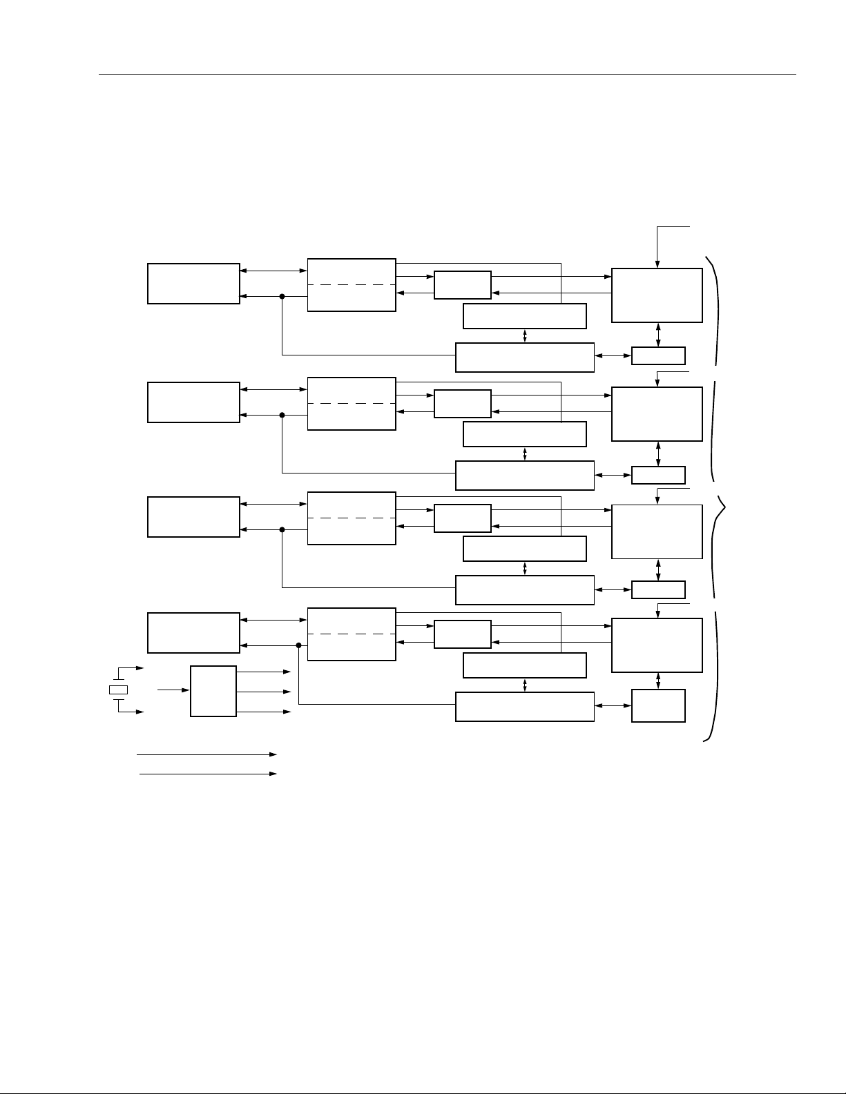
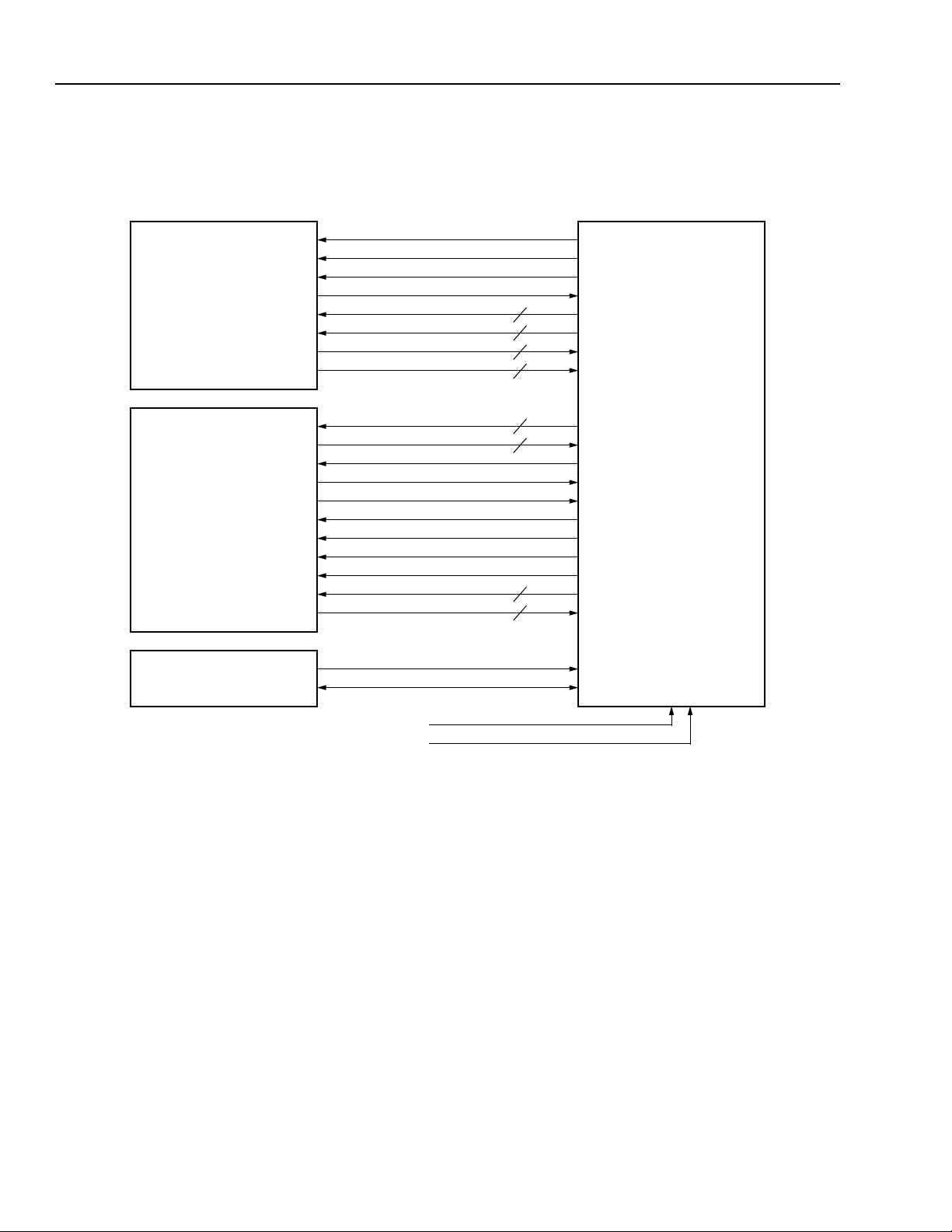
Figure 1 gives a functional overview of the LU3X54FTL
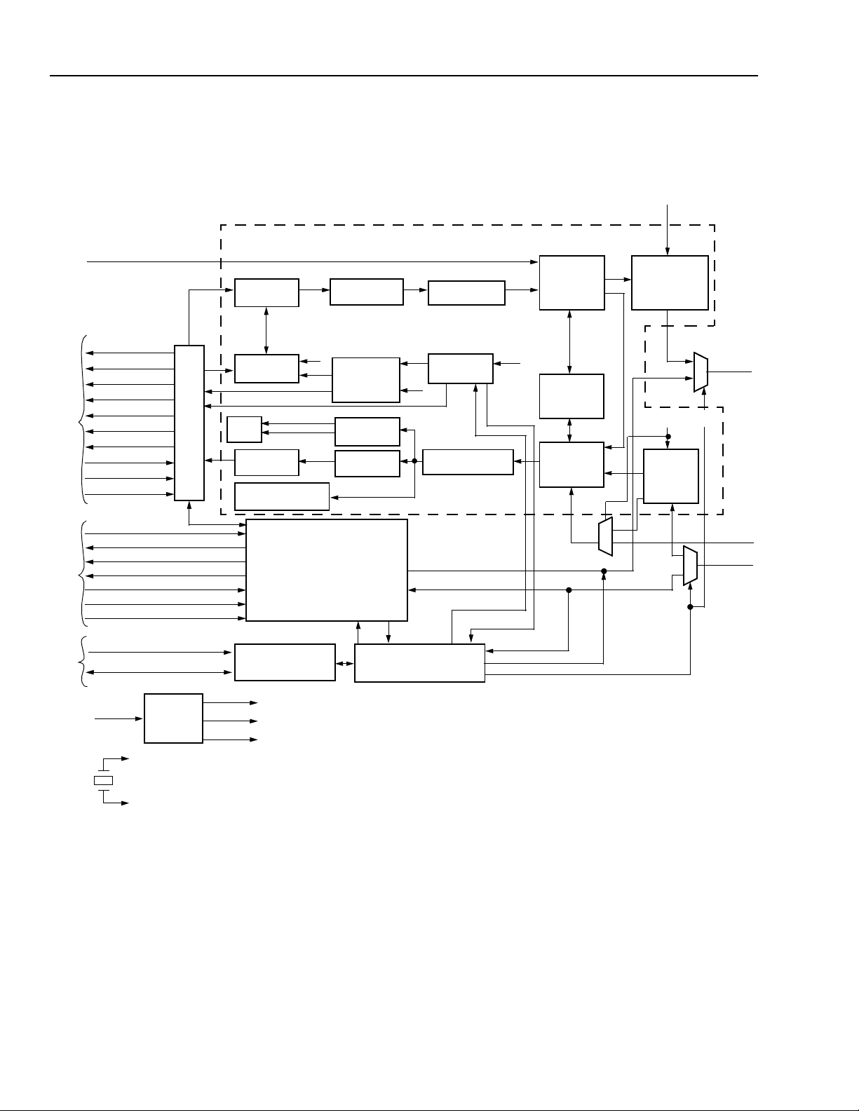
while Figure 2 details its single-channel functions.
Figure 3 shows how the LU3X54FTL sing le-channel
interfaces to the twisted pair (TP).
Clocking
The LU3X54FTL requires an internal 25 MHz clock and
a 20 MHz clock to run the 100Base-TX transceiver and
10Base-T transceiver.
These clocks can be supplied as follows:
■
As separate clock inputs: 25 MHz and 20 MHz.
■
The 20 MHz clock can be internally synthesized from
the 25 MHz clock.
■
The 25 MHz clock can also be internally generated
by an on-chip oscillator if an external crystal is supplied.
The LU3X54FTL will automatically detect if a 25 MHz
clock is supplied, or if a crystal is being used to generate the 25 MHz clock.
The 100 Mbits/s signals are still routed to port A
(TX_CLK25, TXD_100[3:0], TX_ER, RX_ CLK 25,
RXD_100[3:0], RX_DV, and RX_ER).
Lucent Technologies Inc. 5

LU3X54FTL Data Sheet
QUAD-FET for 10Base-T/100Base-TX/FX July 2000
Description
(continued)
Either the on-chip 20 MHz clock synthesizer (default
clock) can be used, or H-DUPLED[A]/CLK20_SEL
(pin 198) can be pulled high (sensed on powerup and
reset) to select the external 20 MHz clock input.
The crystal specifications for the device are listed in
Table 1, an d the crysta l circu it is sh ow n in Fig ure 3 an d
Figure 4.
Table 1. LU3X54FTL Crystal Specifications
Parameter Requirement
Type Quartz Fundamental Mode
Frequency 25 MHz
Stability ±25 ppm, 0—70 °C
Shunt Capacitor 7 pF
Load Capacitor 20 pF
Series Resistance <30 Ω
FX Mode
Each individual port of the LU3X54FTL can be operated in 100Base-FX mode by selecting it through the
pin program option RXLED[D:A]/FX_MODE_EN[D:A],
or through the register bit (register 29, bit 0).
When operating in FX mode, the twisted-pair I/O pins
are reused as the fiber-optic transceiver I/O data pins,
and the fiber-optic signal detect (FOSD) inputs are
enabled.
Figure 4 shows a typical FX port interface. Note that no
additional external components, excluding those
needed by the fiber transceiver, are required.
When a port is placed in FX mode, it will automatically
configure the port for 100Base-FX operation (and the
register bit control will be ignored) such that:
■
The far-end fault signaling option will be enabled.
■
The MLT-3 encoding/decoding will be disabled.
■
Scrambler/descrambler will be disabled.
■
Autonegotiation will be disabled.
■
The signal detect inputs will be activated.
■
10Base-T will be disabled.
6 Lucent Technologies Inc.
Data Sheet LU3X54FTL
July 2000 QUAD-FET for 10Base-T/100Base-TX/FX
Description
(continued)
Functional Block Diagrams
Device Overview
MII/SERIAL
INTERFACE
MII/SERIAL
INTERFACE
MII/SERIAL
INTERFACE
MANAGEMENT
PCS
MANAGEMENT
PCS
MANAGEMENT
PCS
PMA
AUTONEGOTIATION
10 Mbits/s TRANSCEIVER
DRIVER AND FILTERS
PMA
AUTONEGOTIATION
10 Mbits/s TRANSCEIVER
DRIVER AND FILTERS
PMA
AUTONEGOTIATION
TX PMD/
FX PORT
DRIVER AND
FILTERS
MUX
TX PMD/
FX PORT
DRIVER AND
FILTERS
MUX
TX PMD/
FX PORT
DRIVER AND
FILTERS
FX_MODE_EN
FX_MODE_EN
FX_MODE_EN
TP
MAGNETICS
INTERFACE
LSCLK
25 MHz
25 MHz
CRYSTAL
MII/SERIAL
INTERFACE
DPLL
25 MHz
125 MHz
20 MHz
10 Mbits/s TRANSCEIVER
DRIVER AND FILTERS
MANAGEMENT
PMA
PCS
AUTONEGOTIATION
10 Mbits/s TRANSCEIVER
DRIVER AND FILTERS
10 MHz
20 MHz
Figure 1. LU3X54FTL Device Overview
MUX
TX PMD/
FX PORT
DRIVER AND
FILTERS
MUX
FX_MODE_EN
5-5137(F).fr2
Lucent Technologies Inc. 7
LU3X54FTL Data Sheet
QUAD-FET for 10Base-T/100Base-TX/FX July 2000
Description
(continued)
Single-Channel Detail Functions
100 OFF
RX_ER/RXD[4]
MII
INTERFAC E
TX_ER/TXD[4]
SERIAL
INTERFAC E
CRS
COL
RXD[3:0]
RX_DV
RX_CLK
TX_CLK
TXD[3:0]
TX_EN
REF10
RX_CLK
RXD[0]
TX_CLK
TX_EN
TXD[0]
CLK20
TXD[3:0]
MII
4B/5B
ENCODER
TX STATE
MACHINE
CIM
5B/4B
DECODER
FAULT DETECT
100 Mbits/s TRANSCEIVER
FAR-END
FAULT GEN
SD
COLLISION
DETECT
CAR_STAT
RXERR_ST
FAR-END
10 Mbits/s TRANSCEIVER
CARRIER
DETECT
ALIGNER
LC10 LS10
SCRAMBLER
RX STATE
MACHINE
SD
DESCRAMBLER
LC100
LS100
SD
PDT
DCRU
PDR
FX_MODE_EN
PMD
TX/
FIBER PORT
FX_MODE_EN
PMD
RX/
FIBER
PORT
SD
TPOUT
FOSD
±
TPIN
±
MANAGEMENT
INTERFACE
LSCLK
25 MH
MDC
MDIO
DPLL
Z
25 MHz
CRYSTAL
MII
MANAGEMENT
25 MHz
125 MHz
20 MHz
AUTONEGOTIATION
AND LINK MONITOR
Figure 2. LU3X54FTL Single-Channel Detail Functions
5-5136(F).j
8 Lucent Technologies Inc.

Data Sheet LU3X54FTL
July 2000 QUAD-FET for 10Base-T/100Base-TX/FX
Description
(continued)
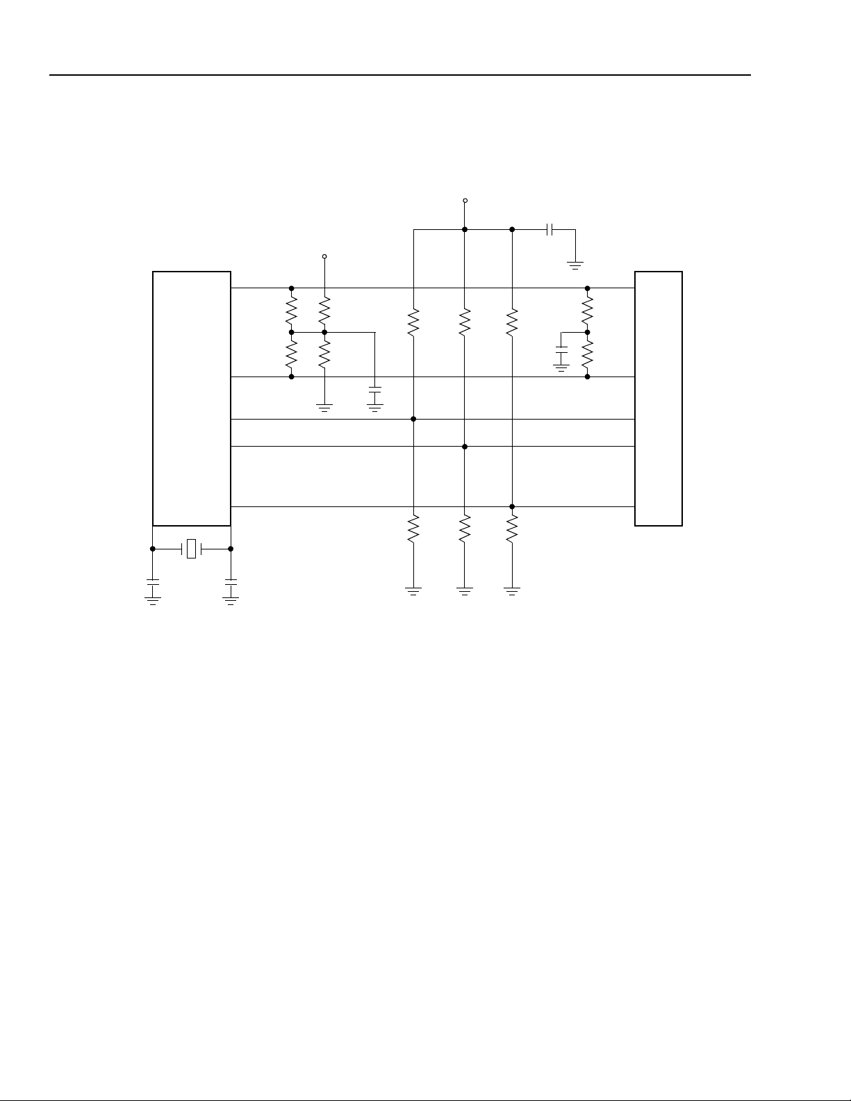
Application Diagrams
Single-Channel Twisted-Pair Interface
LU3X54FTL
88 87
XTALOUT
33 pF 33 pF
25 MHz
TPOUT+
50
50
TPOUT–
TPIN+
50
50
TPIN–
XTALIN
Ω
Ω
Ω
Ω
DDO
V
0.01 µF
220
220
RJ-45
1:1
Ω
Ω
0.01 µF
1:1
0.01 µF
Ω
75
0.01 µF
Ω
75
0.01 µF
75
Ω
Ω
75
0.01 µF
1
2
3
4
5
6
7
8
Figure 3. Typical Single-Channel Twisted-Pair (TP) Interface
5-5433(F).r9
Lucent Technologies Inc. 9
LU3X54FTL Data Sheet
QUAD-FET for 10Base-T/100Base-TX/FX July 2000
Description
(continued)
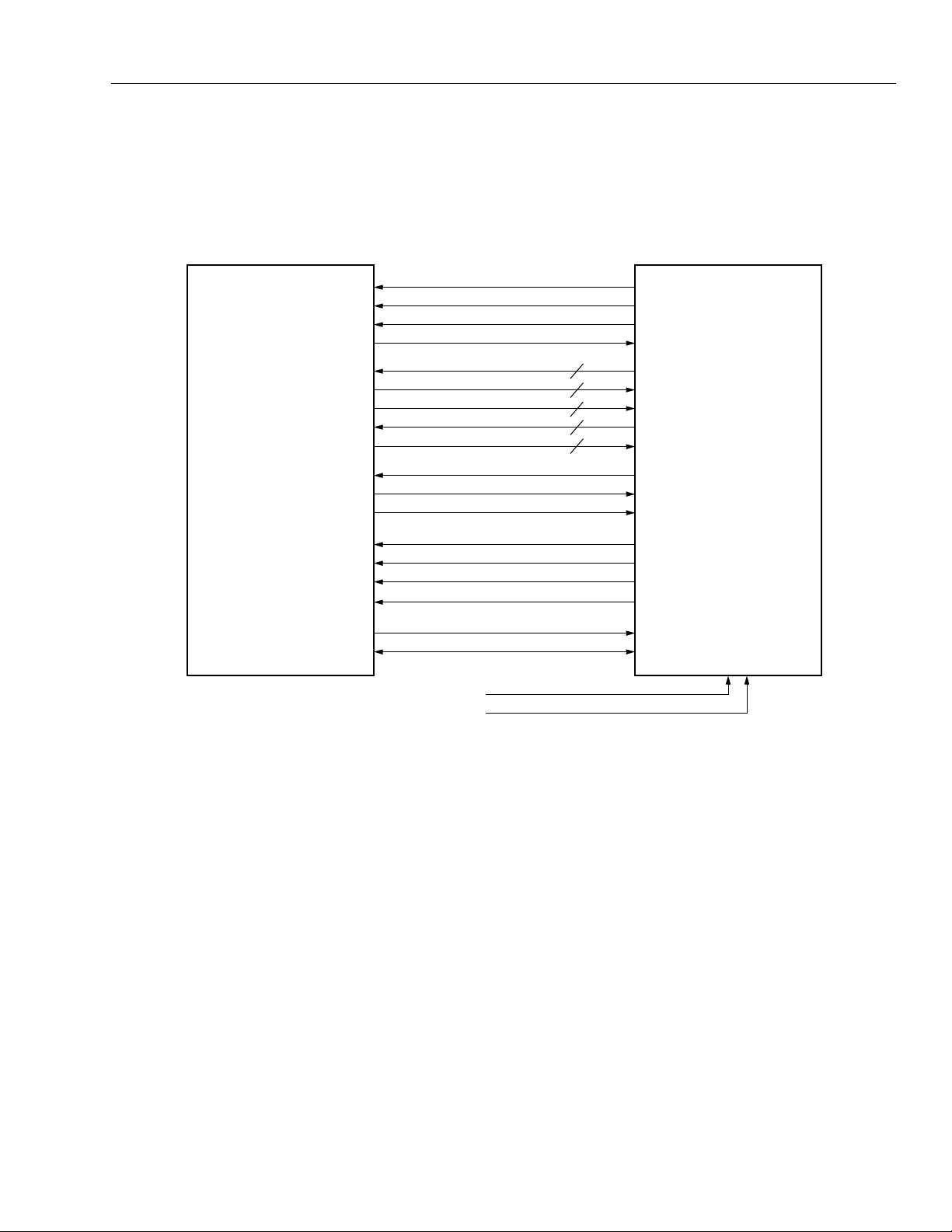
Single-Channel Fiber-Optic Interface
LU3X54FTL
88 87
TPOUT+
50
50
TPOUT–
FOSD
TPIN+
TPIN–
Ω
Ω
DDO
V
Ω
220
Ω
220
0.01 µF
82
130
DDA
V
0.01 µF
TD
Ω
Ω
Ω
82
130
Ω
Ω
Ω
82
0.01 µF
Ω
130
50
50
Ω
TDN
SD
RD
RDN
XTALOUT
33 pF 33 pF
25 MHz
XTALIN
Figure 4. Typical Single-Channel Fiber-Optic Interface
5-5433(F).dr2
10 Lucent Technologies Inc.
Data Sheet LU3X54FTL
July 2000 QUAD-FET for 10Base-T/100Base-TX/FX
Description
(continued)
Block Diagrams
Smart Bused MII Mode
10/100 Mbits/s
SMART
REPEATER
RX_CLK10
RXD_10
TX_CLK10
TXD_10
CRS_10/100
RX_EN10/100
TX_EN10/100
COL_10/100
SECURITY10/100
TX_CLK25
TXD_100[3:0]
TX_ER
RX_CLK25
RXD_100[3:0]
RX_DV
RX_ER
MDC
MDIO
RX_CLK10
RXD_10
TX_CLK10
TXD_10
4
4
4
4
4
CRS_100
RX_EN100
TX_EN100
COL_100
TX_EN10/SECURITY_10/100
TX_CLK25
TXD_100[3:0]
TX_ER
RX_CLK25
RXD_100[3:0]
RX_DV
RX_ER
MDC
MDIO
LU3X54FTL
SMART_MODE_SELECT
BUSED_MII_MODE
Figure 5. Smart 10/100 Mbits/s Bused MII Mode
5-5599.gr1
Lucent Technologies Inc. 11
LU3X54FTL Data Sheet
QUAD-FET for 10Base-T/100Base-TX/FX July 2000
Description
(continued)
Separate Bused MII Mode
10 Mbits/s
REPEATER
100 Mbits/s
REPEATER
RX_CLK10
RXD_10
TX_CLK10
TXD_10
COL_10
CRS_10
RX_EN10
TX_EN10
CRS_100
TX_EN100
TX_CLK25
TXD_100[3:0]
TX_ER
RX_CLK25
RXD_100[3:0]
RX_DV
RX_ER
COL_100
RX_EN100
RX_CLK10
RXD_10
TX_CLK10
4
4
4
4
4
4
4
4
TXD_10
COL_10
CRS_10
RX_EN10
TX_EN10
CRS_100
TX_EN100
TX_CLK25
TXD_100[3:0]
TX_ER
RX_CLK25
RXD_100[3:0]
RX_DV
RX_ER
COL_100
RX_EN100
LU3X54FTL
MANAGEMENT
MDC
MDIO
SMART_MODE_SELECT
BUSED_MII_MODE
MDC
MDIO
Figure 6. Separate 10/100 Mbits/s Bused MII Mode
5-5599.ar7
12 Lucent Technologies Inc.

Data Sheet LU3X54FTL
July 2000 QUAD-FET for 10Base-T/100Base-TX/FX
Pin Information
Pin Diagram for Normal MII Mode
RXD[1][B]
RXD[2][B]
RXD[3][B]
VDD3
MII_EN[B]
TXLED[A]/REF_SEL
VSS
TXLED[B]/SCRAM_DESC_BYPASS
TXLED[C]/ENC_DEC_BYPASS
TXLED[D]/CARIN_EN
VDD167
RXLED[A]/FX_MODE_EN[A]
RXLED[B]/FX_MODE_EN[B]
RXLED[C]/FX_MODE_EN[C]
RXLED[D]/FX_MODE_EN[D]
VDD
COLED[A]
COLED[B]
COLED[C]
COLED[D]
VSS
GNDC
VDDC
VDDC
GNDC
GNDA
ATEST[A]
ATEST[B]
VDDA
VSS
LINKLED[A]/NO_LP
LINKLED[B]/PHYADD[0]
LINKLED[C]PHYADD[1]
LINKLED[D]/PHYADD[2]
SPEEDLED[A]/ISOLATE_MODE
SPEEDLED[B]/BUSED_MII_MODE
SPEEDLED[C]/SMART_MODE_SELECT
SPEEDLED[D]/SPEED
VDD
3ST_EN
AUTO_EN
H_DUPLED[A]/CLK20_SEL
H_DUPLED[B]/CRS_SEL
H_DUPLED[C]/SERIAL_SEL
H_DUPLED[D]/FULL_DUP
VDD
RESET
MODE[0]
MODE[1]
MODE[2]
MODE[3]
VSS
157
158
159
160
161
162
163
164
165
166
168
169
170
171
172
173
174
175
176
177
178
179
180
181
182
183
184
185
186
187
188
189
190
191
192
193
194
195
196
197
198
199
200
201
202
203
204
205
206
207
GNDA
FOSD[C]
FOSD[D]
VDDA
TPIN+/FOIN+[D]
TPIN–/FOIN–[D]
GNDA
VDDA
TPIN+/FOIN+[C]
TPIN–/FOIN–[C]
GNDA
VDDA
BGREF[0]
GNDA
VDDA
TPIN+/FOIN+[B]
TPIN–/FOIN–[B]
GNDA
VDDA
TPIN+/FOIN+[A]
TPIN–/FOIN–[A]
GNDA
VDDA
GNDA
BGREF[1]
GNDD
CLK20
VDDD
GNDAA
VDDAA
TPOUT+/FOOUT+[D]
TPOUT–/FOOUT–[D]
TPOUT+/FOOUT+[C]
TPOUT–/FOOUT–[C]
TPOUT+/FOOUT+[B]
TPOUT–/FOOUT–[B]
TPOUT+/FOOUT+[A]
TPOUT–/FOOUT–[A]
GNDO
VDDO
GNDO
VDDO
GNDM
VDDM
GNDAP
ISET_10
ISET_100
VDDAP
GNDO
VDDO
GNDO
VDDO
208
1
2
3
4
5
6
7
8
9
10
11
12
13
14
15
16
17
18
19
20
21
22
23
24
25
26
27
28
29
30
31
32
33
34
35
36
37
38
39
40
41
42
43
44
45
46
47
48
49
50
51
52
56
55NC54
53
61
60
59
58
57
66
65
64
63
62
71
70
69
68
67
73
72
LU3X54FTL
77
74
102
101
100
99
98
97
96
95
94
93
92
91
90
89
88
87
86
84
83
82
81
80
79
78
103
156
155
154
153
152
151
150
149
148
147
146
145
144
143
142
141
140
139
138
137
136
135
134
133
132
131
130
129
128
127
126
125
124
123
122
121
120
119
118
117
116
115
114
113
112
111
110
109
108
107
106
105
104
VSS
RXD[0][B]
RX_CLK[B]
RX_ER[B]/RXD[4][B]
VDD3
RX_DV[B]
COL[B]
CRS[B]
TX_CLK[B]
VSS
TX_EN[B]
TX_ER[B]/TXD[4][B]
VDD
TXD[3][B]
TXD[2][B]
VSS
TXD[1][B]
TXD[0][B]
MII_EN[A]
VDD3
RXD[3][A]
RXD[2][A]
RXD[1][A]
VSS
RXD[0][A]
RX_CLK[A]
RX_ER[A]/RXD[4][A]
VDD3
RX_DV[A]
COL[A]
CRS[A]
TX_CLK[A]
VSS
TX_EN[A]
TX_ER[A]/TXD[4][A]
VDD3
TXD[3][A]
TXD[2][A]
VSS
TXD[1][A]
TXD[0][A]
VSS
REF10
MDC
MDIO
VDD
MII_EN[D]
RXD[3][D]
RXD[2][D]
RXD[1][D]
VSS
RXD[0][D]
VDD
TXD[3][D]
TX_ER[D]TXD[4][D]
TX_EN[D]
VSS
VDD3
COL[D]
CRS[D]
RX_DV[D]
TX_CLK[D]
RX_CLK[D]
RX_ER[D]/RXD[4][D]
5-5616(F).cr3
VDD3
TXD[3][C]
TX_EN[C]
TX_ER[C]/TXD[4][C]
VSS
COL[C]
CRS[C]
RX_DV[C]
TX_CLK[C]
VSS
MODE[4]
TXD[2][C]
TXD[1][C]
TXD[0][C]
MASK_STAT_INT
VDD3
RX_CLK[C]
RX_ER[C]/RXD[4][C]
VSS
RXD[0][C]
VSS
VDD
CKREF
VDDPLL
RXD[3][C]76RXD[2][C]75RXD[1][C]
MII_EN[C]
VSSPD
VDDPD
VSSPLL
FOSD[B]85FOSD[A]
VSS
TXD[2][D]
TXD[1][D]
TXD[0][D]
XTALOUT
LSCLK/XTALIN
Figure 7. LU3X54FTL Pinout for Normal MII Mode
Lucent Technologies Inc. 13

LU3X54FTL Data Sheet
QUAD-FET for 10Base-T/100Base-TX/FX July 2000
Pin Information
(continued)
Pin Diagram for Bused MII Mode
VDD
3ST_EN
AUTO_EN
H_DUPLED[A]/CLK20_SEL
H_DUPLED[B]/CRS_SEL
195
196
197
198
199
66NC65
64
63NC62
GNDA
FOSD[C]
FOSD[D]
VDDA
TPIN+/FOIN+[D]
TPIN–/FOIN–[D]
GNDA
VDDA
TPIN+/FOIN+[C]
TPIN–/FOIN–[C]
GNDA
VDDA
BGREF[0]
GNDA
VDDA
TPIN+/FOIN+[B]
TPIN–/FOIN–[B]
GNDA
VDDA
TPIN+/FOIN+[A]
TPIN–/FOIN–[A]
GNDA
VDDA
GNDA
BGREF[1]
GNDD
CLK20
VDDD
GNDAA
VDDAA
TPOUT+/FOOUT+[D]
TPOUT–/FOOUT–[D]
TPOUT+/FOOUT+[C]
TPOUT–/FOOUT–[C]
TPOUT+/FOOUT+[B]
TPOUT–/FOOUT–[B]
TPOUT+/FOOUT+[A]
TPOUT–/FOOUT–[A]
GNDO
VDDO
GNDO
VDDO
GNDM
VDDM
GNDAP
ISET_10
ISET_100
VDDAP
GNDO
VDDO
GNDO
VDDO
VSS
MODE[3]
207
208
1
2
3
4
5
6
7
8
9
10
11
12
13
14
15
16
17
18
19
20
21
22
23
24
25
26
27
28
29
30
31
32
33
34
35
36
37
38
39
40
41
42
43
44
45
46
47
48
49
50
51
52
53
VDD
RESET
MODE[0]
MODE[1]
MODE[2]
206
55NC54
H_DUPLED[D]/FULL_DUP
H_DUPLED[C]/SERIAL_SEL
200
201
202
203
204
205
61
59
58
56
COLED[D]
176
COLED[C]
175
COLED[B]
174
COLED[A]
173
VDD
172
VSS
ATEST[A]
ATEST[B]
LINKLED[A]/NO_LP
LINKLED[B]/PHYADD[0]
SPEEDLED[D]/SPEED
194
LINKLED[C]PHYADD[1]
LINKLED[D]/PHYADD[2]
SPEEDLED[A]/ISOLATE_MODE
SPEEDLED[B]/BUSED_MII_MODE
SPEEDLED[C]/SMART_MODE_SELECT
183
184
185
186
187
188
189
190
191
192
193
182
GNDC
180
181
179
GNDC
177
178
VSS
VDDC
VDDC
GNDA
VDDA
LU3X54FTL
89
88
87
86
84
83
82
81
80
79
78
77
75
74
73
72NC71NC70
69NC68
67
RXLED[D]/FX_MODE_EN[D]
171
VDD167
TXLED[D]/CARIN_EN
RXLED[A]/FX_MODE_EN[A]
RXLED[B]/FX_MODE_EN[B]
RXLED[C]/FX_MODE_EN[C]
168
169
170
94
92
91
TXLED[A]/REF_SEL
TXLED[C]/ENC_DEC_BYPASS
TXLED[B]/SCRAM_DESC_BYPASS
162
163
164
165
166
99NC98
97
96NC95
RX_EN100[B]/RX_EN10/100[B]
161
100
VDD3
160
102NC101
NC
157NC158NC159
VSS
156
RXD_10
155
RX_CLK10
154
NC
153
VDD3
152
NC
151
COL_100[B]/COL_10/100[B]
150
CRS_100[B]/CRS_10/100[B]
149
TX_CLK10
148
VSS
147
TX_EN100[B]/TX_EN10/100
146
NC
145
VDD
144
NC
143
NC
142
VSS
141
NC
140
TXD_10
139
RX_EN100[A]/RX_EN10/100[A]
138
VDD3
137
RXD_100[3]
136
RXD_100[2]
135
RXD_100[1]
134
VSS
133
RXD_100[0]
132
RX_CLK25
131
RX_ER
130
VDD3
129
RX_DV
128
COL_100[A]/COL_10/100[A]
127
CRS_100[A]/CRS_10/100[A]
126
TX_CLK25
125
VSS
124
TX_EN100[A]/TX_EN10/100
123
TX_ER
122
VDD3
121
TXD_100[3]
120
TXD_100[2]
119
VSS
118
TXD_100[1]
117
TXD_100[0]
116
VSS
115
REF10
114
MDC
113
MDIO
112
VDD
111
RX_EN100[D]/RX_EN10/100[D]
110
CRS_10[D]
109
CRS_10[C]
108
CRS_10[B]
107
VSS
106
CRS_10[A]
105
104NC103
VSS
VDD3
VSS
COL_10[B]
COL_10[A]
RX_EN10[D]60RX_EN10[C]
VDD3
VSS
TX_EN100[C]/TX_EN10/100
COL_100[C]/COL_10/100[C]
CRS_100[C]/CRS_10/100[C]
VSS
MODE[4]
RX_EN10[B]57RX_EN10[A]
MASK_STAT_INT
VSS
VDD
CKREF
VDDPLL
COL_10[D]76COL_10[C]
RX_EN100[C]/RX_EN10/100[C]
VSSPLL
VDDPD
VSSPD
FOSD[B]85FOSD[A]
VSS
XTALOUT
LSCLK/XTALIN
TX_EN10[B]/SECURITY_10/10090TX_EN10[A]/SECURITY_10/100
VSS
VDD
TX_EN100[D]/TX_EN10/100
CRS_100[D]/CRS_10/100[D]
TX_EN10[D]/SECURITY_10/10093TX_EN10[C]/SECURITY_10/100
NC
VDD3
COL_100[D]/COL_10/100[D]
5-5616(F).dr2
Figure 8. LU3X54FTL Pinout for Bused MII Mode
14 Lucent Technologies Inc.

Data Sheet LU3X54FTL
July 2000 QUAD-FET for 10Base-T/100Base-TX/FX
Pin Information
(continued)
Pin Maps
Table 2. LU3X54FTL Pin Maps
Normal Mode Pins Bused Mode Pins 10/100 Mbits/s Smart Mode Pins Separate Mode Pins
RXD[3:0][D] CRS_10[D:A] Not used CRS_10
CRS[D:A] CRS_100[D:A] CRS_10/100 CRS_100
TXD[3:0][C] RX_EN10/100 Not used RX_EN10
MII_EN[D:A] RX_EN100[D:A] RX_EN10/100 RX_EN100
TXD[3:0][D] TX_EN10[D:A] SECURITY_10/100 TX_EN10
TX_EN[D:A] TX_EN100[D:A] TX_EN10/100 TX_EN100
RXD[3:0][C] COL_10[D:A] Not used COL_10
COL[D:A] COL_100[D:A] COL_10/100 COL_100
SPEEDLED[C] SMART_MODE_SELECT SMART_MODE_SELECT SMART_MODE_SELECT
SPEEDLED[B] BUSED_MII_MODE BUSED_MII_MODE BUSED_MII_MODE
TX_CLK[A] TX_CLK25 TX_CLK25 TX_CLK25
TX_CLK[B] TX_CLK10 TX_CLK10 TX_CLK10
RX_CLK[B] RX_CLK10 RX_CLK10 RX_CLK10
RX_CLK[A] RX_CLK25 RX_CLK25 RX_CLK25
RXD[0][B] RXD_10 RXD_10 RXD_10
RXD[3:0][A] RXD_100[3:0] RXD_100 RXD_100
RX_DV[A] RX_DV RX_DV RX_DV
RX_ER[A] RX_ER RX_ER RX_ER
TXD[0][B] TXD_10 TXD_10 TXD_10
TXD[3:0][A] TXD_100[3:0] TXD_100 TXD_100
TX_ER[A]/TXD[4][A] TX_ER TX_ER TX_ER
Lucent Technologies Inc. 15

LU3X54FTL Data Sheet
QUAD-FET for 10Base-T/100Base-TX/FX July 2000
Pin Information
(continued)
Pin Descriptions
This section describes the LU3X54FTL signal pins. Note that any register bit referenced includes the register number and bit position. For example, register bit [29.8] is register 29, bit 8.
Table 3. MII/Serial Interface Pins in Normal MII Mode (Four Separate MII Ports)
Pin Signal Type Description
100
67
150
127
99
66
149
126
104
71
154
131
109
76
159
136
108
75
158
135
107
74
157
134
105
72
155
132
101
68
151
128
103
70
153
130
COL[D:A] O
CRS[D:A] O
RX_CLK[D:A] O
RXD[3:0][D:A] O
RX_DV[D:A] O
RX_ER[D:A]/
RXD[4][D:A]
Collision Detect.
This signal signifies in half-duplex mode that a collision
has occurred on the network. COL is asserted high whenever there is
transmit and receive activity on the UTP media. COL is the logical AND of
TX_EN and receive activity, and is an asynchronous output. When
SERIAL_SEL is high and in 10Base-T mode, this signal indicates the jabber timer has expired.
Carrier Sense.
When CRS_SEL is low, this signal is asserted high when
either the transmit or receive medium is nonidle. This signal remains
asserted throughout a collision condition. When CRS_SEL is high, CRS is
asserted on receive activity only . CRS_SEL is set via the MII management
interface or the CRS_SEL pin.
Receive Clock.
25 MHz clock output in 100 Mbits/s mode, 2.5 MHz output
in 10 Mbits/s nibble mode, 10 MHz in 10 Mbits/s serial mode. RX_CLK has
a worst-case 45/55 duty cycle. RX_CLK provides the timing reference for
the transfer of RX_DV, RXD, and RX_ER signals.
Receive Data
. 4-bit parallel data outputs that are synchronous to RX_CLK.
When RX_ER[D:A] is asserted high in 100 Mbits/s mode, an error code will
be presented on RXD[3:0][D:A] where appropriate. The codes are as follows:
■
Packet errors: ERROR_CODES = 2h.
■
Link errors: ERROR_CODES = 3h. (Packet and link error codes will only
be repeated if registers [29.9] and [29.8] are enabled.)
■
Premature end errors: ERROR_CODES = 4h.
■
Code errors: ERROR_CODES = 5h.
When SERIAL_SEL is active-high and 10 Mbits/s mode is selected, RXD[0]
is used for data output and RXD[3:1] are 3-stated.
Receive Data Valid.
When this pin is high, it indicates the LU3X54FTL is
recovering and decoding valid nibbles on RXD[3:0], and the data is synchronous with RX_CLK. RX_DV is synchronous with RX_CLK. This pin is
not used in serial 10 Mbits/s mode.
Receive Error.
O
When high, RX_ER indicates the LU3X54FTL has detected
a coding error in the frame presently being transferred. RX_ER is synchronous with RX_CLK.
Receive Data[4].
When encoder/decoder bypass (ENC_DEC_BYP ASS) is
selected through the MII management interface, this output serves as the
RXD[4] output. This pin is only valid when the LU3X54FTL is in 100 Mbits/s
mode.
16 Lucent Technologies Inc.

Data Sheet LU3X54FTL
July 2000 QUAD-FET for 10Base-T/100Base-TX/FX
Pin Information
Table 3. MII/Serial Interface Pins in Normal MII Mode (Four Separate MII Ports)
Pin Signal Type Description
98
65
148
125
93, 60
143, 120
92, 59
142, 119
90, 57
140, 117
89, 56
139, 116
96
63
146
123
95
62
145
122
110
78
161
138
TX_CLK[D:A] O
TXD[3:0][D:A] I
(continued)
TX_EN[D:A] I
TX_ER[D:A]/
TXD[4][D:A]
MII_EN[D:A] I
Transmit Clock.
in 10 Mbits/s MII mode, 10 MHz output in 10 Mbits/s serial mode. TX_CLK
provides timing reference for the transfer of the TX_EN, TXD, and TX_ER
signals sampled on the rising edge of TX_CLK.
Transmit Data.
SERIAL_SEL is active-high and 10 Mbits/s mode is selected, only
TXD[0][D:A] are valid.
T ransmit Enable.
on TXD[3:0]. TX_EN is synchronous with TX_CLK. When SERIAL_SEL is
active-high and 10 Mbits/s mode is selected, this pin indicates there is valid
data on TXD[0].
Transmit Coding Error.
I
to intentionally corrupt the byte being transmitted across the MII (00100 will
be transmitted).
Transmit Data[4].
serves as the TXD[4] input. When in 10 Mbits/s mode and SERIAL_SEL is
active-high, this pin is ignored.
MII Enable.
for each channel must be tied high to enable each individual port being
used.
25 MHz clock output in 100 Mbits/s mode, 2.5 MHz output
4-bit parallel input synchronous with TX_CLK. When
When driven high, this signal indicates there is valid data
When driven high, this signal causes the encoder
When the encoder/decoder bypass bit is set, this input
For normal MII mode of operation (nonbused mode), MII_EN
(continued)
Lucent Technologies Inc. 17

LU3X54FTL Data Sheet
QUAD-FET for 10Base-T/100Base-TX/FX July 2000
Pin Information
(continued)
When operating in bused MII mode, 100 Mbits/s data is bused to MII port A, and 10 Mbits/s data is bused to MII
port B.
Table 4. MII/Serial Interface Pins in Bused MII Mode
Pin Signal Type Description
125 TX_CLK25 O
148 TX_CLK10 O
109
108
107
105
99
66
149
126
154 RX_CLK10 O
131 RX_CLK25 O
155 RXD_10 O
CRS_10[D:A] O
CRS_100[D:A]/
CRS_10/100[D:A]
Shared Transmit Clock (25 MHz).
TX_CLK25 provides timing reference for the transfer of the TX_EN100,
TXD_100, and TX_ER signals that are sampled on the rising edge of
TX_CLK25.
Shared Transmit Clock (10 MHz).
mode. TX_CLK10 provides timing reference for the transfer of the TX_EN10
and TXD_10 signals that are sampled on the rising edge of TX_CLK10.
When operating in 10 Mbits/s bused mode, the REF10 input clock must be
used, and the REF_SEL pin must be pulled high through a 4.7 kΩ resistor
(TXLED[A] pin).
Carrier Sense—10 Mbits/s Mode.
asserted high when either the transmit or receive medium is nonidle. This signal remains asserted throughout a collision condition. When CRS_SEL is
high, CRS_10 is asserted on receive activity only. CRS_SEL is set via the MII
management interface or the CRS_SEL pin.
When SMART_MODE_SELECT is asserted, the LU3X54FTL will internally
OR together the CRS_10 and the CRS_100 signals and output them on the
CRS_100 signals.
O
Carrier Sense—100 Mbits/s Mode.
asserted high when either the transmit or receive medium is nonidle. This signal remains asserted throughout a collision condition. When CRS_SEL is
high, CRS_100 is asserted on receive activity only. CRS_SEL is set via the MII
management interface or the CRS_SEL pin.
Carrier Sense—10/100 Mbits/s Smart Mode.
SMART_MODE_SELECT is asserted, the LU3X54FTL will internally OR
together the CRS_10 and the CRS_100 signals and output them on the
CRS_100 signals.
Shared Receive Clock.
RX_CLK10 has a worst-case 45/55 duty cyc le . RX_CLK10 pro vides the timing
reference for the transfer of RXD_10 when in the 10 Mbits/s mode. This signal
is sampled on the rising edge of RX_CLK10.
Shared Receive Clock.
RX_CLK25 has a worst-case 45/55 duty cyc le . RX_CLK25 pro vides the timing
reference for the transfer of RX_DV, RXD_100, and RX_ER signals when in
the 100 Mbits/s mode. These signals are sampled on the rising edge of
RX_CLK100.
Shared Receive Data.
edge of RX_CLK10.
10 MHz clock output in 10 Mbits/s serial mode.
25 MHz clock output in the 100 Mbits/s mode.
Serial data output that is synchronous to the falling
25 MHz clock output in 100 Mbits/s mode.
10 MHz clock output in 10 Mbits/s serial
When CRS_SEL is low, this signal is
When CRS_SEL is low, this signal is
When
18 Lucent Technologies Inc.

Data Sheet LU3X54FTL
July 2000 QUAD-FET for 10Base-T/100Base-TX/FX
Pin Information
(continued)
When operating in bused MII mode, 100 Mbits/s data is bused to MII port A, and 10 Mbits/s data is bused to MII
port B.
Table 4. MII/Serial Interface Pins in Bused MII Mode
(continued)
Pin Signal Type Description
136
135
134
132
RXD_100[3:0] O
Shared Receive Data.
4-bit parallel data outputs that are synchronous to the
falling edge of RX_CLK25. When RX_ER is asserted high, an error code will
be presented on RXD_100[3:0] where appropriate. The codes are as follows:
Packet errors, ERROR_CODES = 2h.
■
Link errors, ERROR_CODES = 3h (packet and link error codes will only be
■
repeated if registers [29.9] and [29.8] are enabled).
Premature end errors, ERROR_CODES = 4h.
■
Code errors, ERROR_CODES = 5h.
■
60
59
57
56
RX_EN10[D:A] I
Receive Enable—10 Mbits/s Mode.
When SMART_MODE_SELECT is not
enabled and RX_EN10 is driven high, its channel’s data and clock (RXD0 and
RX_CLK) are driven onto the shared serial bus. If the indiv idual channel is not
configured for 10 Mbits/s mode, this input will be ignored. When RX_EN10s
are all set low, the serial bus will float.
Care should be taken that no more than one RX_EN is asserted at a
Note:
time.
110
78
RX_EN100[D:A]/
RX_EN10/100[D:A]
161
138
128 RX_DV O
130 RX_ER O
139 TXD_10 I
120
TXD_100[3:0] I
119
117
116
When SMART_MODE_SELECT is enabled, these pins are ignored.
I
Receive Enable—100 Mbits/s Mode.
When SMART_MODE_SELECT is not
enabled and RX_EN100 is driven high, its channel’s data, clock, and receive
data valid signals (RXD_100, RX_DV, RX_ER, and RX_CLK25) are driven
onto the shared MII bus. If the individual channel is not configured for
100 Mbits/s mode, this input will be ignored. When RX_EN100s are all set low,
the MII bus will float.
Care should be taken that no more than one RX_EN is asserted at a
Note:
time.
Receive Enable—10/100 Mbits/s Smart Mode.
When
SMART_MODE_SELECT is asserted and RX_EN100 is driven high, its channel’s data, clock, and receive data valid signals [RXD, RX_ER (100 Mbits/s
only), RX_D V (100 Mbits/s only), and RX_CLK] are driven onto the shared b us
corresponding to the speed of the channel.
Shared Receive Data Valid.
When this pin is driven high, it indicates that the
LU3X54FTL is recovering and decoding valid nibb les on RXD[3:0] and that the
data is synchronous with RX_CLK. RX_D V is synchronous with RX_CLK. This
pin is not used in serial 10 Mbits/s mode.
Shared Receive Error.
When asserted high, it indicates that the LU3X54FTL
has detected a coding error in the frame presently being transf erred. RX_ER is
synchronous with RX_CLK25. This signal is not used in 10 Mbits/s mode.
Shared Transmit Data.
Shared Transmit Data.
10 Mbits/s serial input synchronous with TX_CLK10.
4-bit parallel input synchronous with TX_CLK25.
Lucent Technologies Inc. 19

LU3X54FTL Data Sheet
QUAD-FET for 10Base-T/100Base-TX/FX July 2000
Pin Information
(continued)
When operating in bused MII mode, 100 Mbits/s data is bused to MII port A, and 10 Mbits/s data is bused to MII
port B.
Table 4. MII/Serial Interface Pins in Bused MII Mode
Pin Signal Typ e Description
93
92
90
89
96
63
146
123
122 TX_ER I
76
75
74
72
TX_EN10/[D:A]/
SECURITY_10/100
TX_EN100[D:A]/
TX_EN10/100
COL_10[D:A] O
I
Transmit Enable—10 Mbits/s Mode.
that there is valid data on TXD when the corresponding channel is in
10 Mbits/s serial mode.
Security for 10/100 Mbits/s Smart Mode.
is enabled, these pins are redefined to be the security input pins for both
10 Mbits/s and 100 Mbits/s. When security is activated, the LU3X54FTL will
ignore the transmit data, and a fixed pattern is transmitted (all 1s for 10Base-T,
alternating 1, 0 for 100TX).
Security should not be asserted until after the entire preamble has been transmitted. When in smart mode, the 10 Mbits/s transmit channels will be enabled
through the TX_EN100 inputs.
I
T ransmit Enable—100 Mbits/s Mode.
enabled and TX_EN100 is driven high, this signal indicates that there is valid
data on TXD_100[3:0] when in 100 Mbits/s mode. If the individual channel is
not configured for 100 Mbits/s mode, this input will be ignored.
Transmit Enable—10/100 Mbits/s Smart Mode.
SMART_MODE_SELECT is asserted and TX_EN100 is driven high, this signal indicates that its channel ’s input data is valid. The input data is s elected by
the speed of the corresponding channel.
Shared Transmit Coding Error.
encoder to intentionally corrupt the byte being transmitted across the MII
(00100 will be transmitted). This signal is not used in 10 Mbits/s mode.
Collision Detect for 10 Mbits/s Mode.
fies that a collision has occurred on the network. COL_10 is asserted high
whenever there is transmit and receive activity on the UTP media. COL_10 is
the logical AND of TX_EN and receive activity, and it is an asynchronous output.
(continued)
When driven high, this signal indicates
When SMART_MODE_SELECT
When SMART_MODE_SELECT is not
When
When asserted high, this signal causes the
In half-duplex mode, this signal signi-
When SERIAL_SEL is high and in 10Base-T mode, this signal indicates that
the jabber timer has expired. When SMART_MODE_SELECT is asserted, the
LU3X54FTL will internally OR together the COL_10 and COL_100 signals and
output them on the COL_100 pins.
100
67
150
127
COL_100[D:A]/
COL_10/100[D:A]
O
Collision Detect for 100 Mbits/s Mode.
fies that a collision has occurred on the network. COL_100 is asserted high
whenev er there is trans mit and receiv e activity on the UTP media. COL_100 is
the logical AND of TX_EN and receive activity, and it is an asynchronous output.
Collision Detect for 10/100 Mbits/s Smart Mode.
high and in 10Base-T mode, this signal indicates that the jabber timer has
expired. When SMART_MODE_SELECT is asserted, the LU3X54FTL will
internally OR together the COL_10 and COL_100 signals and output them on
the COL_100 pins.
In half-duplex mode, this signal signi-
When SERIAL_SEL is
20 Lucent Technologies Inc.

Data Sheet LU3X54FTL
July 2000 QUAD-FET for 10Base-T/100Base-TX/FX
Pin Information
(continued)
When operating in bused MII mode, 100 Mbits/s data is bused to MII port A, and 10 Mbits/s data is bused to MII
port B.
Table 4. MII/Serial Interface Pins in Bused MII Mode
Pin Signal Type Description
65
68
70
71
98
101
103
104
62
95
140
142
143
145
151
153
157
158
159
NC O
NC I
No Connect.
No Connect.
(continued)
Do not connect these pins.
These inputs should be grounded.
Lucent Technologies Inc. 21

LU3X54FTL Data Sheet
QUAD-FET for 10Base-T/100Base-TX/FX July 2000
Pin Information
Table 5. MII Management Pins
Pin Signal Type Description
113 MDC I
112 MDIO I/O
53 MASK_STAT_INT O
Table 6. 10/100 Mbits/s Twisted-Pair (TP) Interface Pins
Pin Signal Type Description
(continued)
Management Data Clock.
data on the MDIO signal. This signal may be asynchronous to RX_CLK and
TX_CLK. The maximum clock rate is 12.5 MHz.
When running MDC above 6.25 MHz, MDC must be synchronous with
LSCLK and have a setup time of 15 ns and a hold time of 5 ns with respect
to LSCLK. When using an external crystal instead of an LSCLK input, the
maximum MDC rate is 6.25 MHz.
Management Data Input/Output.
status information between the LU3X54FTL and the station management.
Control information is driven by the station management synchronous with
MDC. Status information is driven by the LU3X54FTL synchronous with
MDC. This pin requires an external 1.5 kΩ pull-up resistor.
Maskable Status Interrupt.
change in status as defined in Table 22.
This is the timing reference for the transfer of
This I/O is used to transfer control and
This pin will go high whenever there is a
5
9
16
20
6
10
17
21
32
36
46
50
33
37
47
51
3
2
85
84
TPIN+/
FOIN+[D:A]
TPIN–/
FOIN–[D:A]
TPOUT+/
FOOUT+[D:A]
TPOUT–/
FOOUT–[D:A]
FOSD[D:A] I
Received Data.
I
Manchester data from magnetics.
Fiber-Optic Data Input.
ECL data from fiber transceiver.
Received Data.
I
Manchester data from magnetics.
Fiber-Optic Data Input.
ECL data from fiber transceiver.
Transmit Data.
O
Manchester data to magnetics.
Fiber-Optic Data Output.
ECL compatible data to fiber transceiver.
Transmit Data.
O
Manchester data to magnetics.
Fiber-Optic Data Output.
ECL compatible data to fiber transceiver.
Fiber-Optic Signal Detect.
whether or not the fiber-optic receive pairs (FOIN±) are receiving valid signal
levels. These inputs are ignored when not in fiber mode, and should be
grounded.
Positiv e differential received 125 Mbaud MLT3, or 10 Mbaud
Positive differential received 125 Mbaud pseudo-
Negative differential received 125 Mbaud ML T3 or 10 Mbaud
Negative differential received 125 Mbaud pseudo-
Positive differential transmit 125 Mbaud MLT3 or 10 Mbaud
Positive differential transmit 125 Mbaud pseudo-
Negative differential transmit 125 Mbaud MLT3 or 10 Mbaud
Negative differential transmit 125 Mbaud pseudo-
Pseudo-ECL input signal which indicates
22 Lucent Technologies Inc.

Data Sheet LU3X54FTL
July 2000 QUAD-FET for 10Base-T/100Base-TX/FX
Pin Information
(continued)
Table 7. Miscellaneous Pins
Pin Signal Type Description
81 CKREF I
Clock Reference.
Connect this pin to a 1 nF ± 10% capacitor to
ground.
184
ATEST[B:A] O
Reserved.
For normal operation, leave these pins unconnected.
183
197 AUTO_EN I
Autonegotiation Enable.
When this pin is high, autonegotiation is
enabled. Pulsing this pin will cause autonegotiation to restart. This
input has the same function as register 0, bit 12. This input and the register bit are ANDed together.
1, 7,
GND/V
SS
PWR
Ground.
(38 pins.)
11, 14,
18, 22,
24, 26,
29, 31,
35, 39,
41, 45,
49, 58,
64, 73,
79, 82,
86, 91,
97, 106,
115, 118,
124, 133,
141, 147,
156, 163,
177, 178,
181, 182,
186, 208
4, 8, 12,
V
DD
PWR
5.0 V ± 5% power supply (27 pins.)
DD
V
.
15, 19,
23, 28,
30, 34,
38, 40,
44, 48,
52, 77,
80, 83,
94, 111,
144, 167,
172, 179,
180, 185,
195, 202
61, 69,
V
DD3
PWR
3.3 V ± 5% or 5.0 V ± 5% power supply (8 pins.)
DD3
V
.
102, 121,
129, 137,
152, 160
196 3ST_EN I
3-State Enable.
When this pin is high, all digital outputs will be
3-stated. For normal operating conditions, pull this pin low.
25
13
42 ISET_10 I
BGREF[1:0] I
Band Gap Reference.
Connect these pins to a 24.9 kΩ ± 1% resistor
to ground. The parasitic load capacitance should be less than 15 pF.
Current Set 10 Mbits/s.
An external resistor (22.1 kΩ) is placed from
this pin to ground to set the 10 Mbits/s TP driver transmit output level.
Lucent Technologies Inc. 23

LU3X54FTL Data Sheet
QUAD-FET for 10Base-T/100Base-TX/FX July 2000
Pin Information
Table 7. Miscellaneous Pins
Pin Signal Type Description
43 ISET_100 I
114 REF10 I
27 CLK20 I
166 TXLED[D]/
165 TXLED[C]/
ENC_DEC_BYPASS
(continued)
CARIN_EN
(continued)
Current Set 100 Mbits/s.
placed from this pin to ground to set the 100 Mbits/s TP driver transmit
output level.
10 MHz Input Clock.
mode for phase alignment. When used, TX_CLK will be driven from
REF10. If not used, let this pin float.
20 MHz Input Clock.
45%—55% duty cycle. If the internal 20 MHz clock synthesizer is being
used, ground this pin (default).
I/O
Transmit LED[D].
nal buffers are necessary to drive the LEDs.
Carrier Integrity Enable.
through a 4.7 kΩ resistor, it will enable the carrier integrity function of
register 29, bit 3, if station management is unavailable.
This pin has an internal 50 kΩ pull-down resistor for normal operation
(CARIN_EN is disabled). This input and register bits [29.3] are ORed
together.
I/O
Transmit LED[C].
nal buffers are necessary to drive the LEDs.
Encoder/Decoder Bypass.
high through a 4.7 kΩ resistor, it will enable the ENC_DEC_BYPASS
function of register 29, bit 6, if station management is unavailable.
This pin indicates transmit activity on port D. Exter-
This pin indicates transmit activity on port C. Exter-
An external resistor (nominally 24.9 kΩ) is
Optional reference clock for 10 Mbits/s repeater
20 MHz (±100 ppm) TTL level clock with
At powerup or reset, if this pin is pulled high
At powerup or reset, if this pin is pulled
164 TXLED[B]/
SCRAM_DESC_BYPASS
162 TXLED[A]/
REF_SEL
This pin has an internal 50 kΩ pull-down resistor for normal operation
(encoder/decoder ON). This input and the register bit [29.6] are ORed
together enabling the encoder/decoder bypass function for all four
channels.
I/O
Transmit LED[B].
nal buffers are necessary to drive the LEDs.
Scrambler/Descrambler Bypass.
be used to enable the SCRAM_DESC_BYPASS function by pulling this
pin high through a 4.7 kΩ resistor, if station management is unavailable. This is the same function as register 29, bit 4.
This pin has an internal 50 kΩ pull-down resistor for normal operation
(scrambler/descrambler ON). This input and the register bit [29.4] are
ORed together during powerup and reset.
I/O
Transmit LED[A].
nal buffers are necessary to drive the LEDs.
Reference Select.
10 MHz reference input of pin REF10 by pulling it high through a 4.7 kΩ
resistor , if station management is unavai lable. This is the same function
as register 30, bit 2.
This pin has an internal 50 kΩ pull-down resistor for normal operation
(REF10 not used). This input and the register bit are ORed together.
This pin indicates transmit activity on port B. Exter-
At powerup or reset, this pin may
This pin indicates transmit activity on port A. Exter-
At powerup, this pin may be used to select the
24 Lucent Technologies Inc.

Data Sheet LU3X54FTL
July 2000 QUAD-FET for 10Base-T/100Base-TX/FX
Pin Information
Table 7. Miscellaneous Pins
Pin Signal Type Description
171—168 RXLED[D:A]/
176—173 COLED[D:A] O
190 LINKLED[D]/
189 LINKLED[C]/
(continued)
(continued)
FX_MODE_EN[D:A]
PHYADD[2]
PHYADD[1]
I/O
Receive LED[D:A].
are necessary to drive the LEDs.
FX Mode Enable.
4.7 k
resistor, this pin will enable the FX mode (10Base-T and
Ω
100Base-TX disabled). When pulled low, it will enable 10Base-T and
100Base_TX modes (100Base-FX mode disabled). These pins are
ORed with register 29, bit 0 [29.0].
These pins have internal 50 k
Collision LED.
are necessary to drive the LEDs.
Channels A and B have internal 50 k
channels C and D.
I/O
Link LED[D]
buffers are necessary to drive the LEDs.
PHY Address 2.
address bit 2.
If this pin is pulled high through a 50 kΩ resistor, it will set PHYADD[2]
to a 1. If this pin is pulled low through a 50 kΩ resistor, it will set
PHYADD[2] to a 0.
I/O
Link LED[C].
buffers are necessary to drive the LEDs.
PHY Address 1.
address bit 1.
This pin indicates receive activity. External buffers
At powerup or reset, when pulled high through a
Ω
This pin indicates collisi on occurrence. External buff ers
. This pin indicates good link status on port D. External
At powerup or reset, this pin is used to set the PHY
This pin indicates good link status on port C. External
At powerup or reset, this pin is used to set the PHY
pull-down resistors.
pull-down resistors but not
Ω
188 LINKLED[B]/
PHYADD[0]
187 LINKLED[A]/
NO_LP
If this pin is pulled high through a 50 kΩ resistor, it will set PHYADD[1]
to a 1. If this pin is pulled low through a 50 kΩ resistor, it will set
PHYADD[1] to a 0.
I/O
Link LED[B].
buffers are necessary to drive the LEDs.
PHY Address 0.
PHY address bit 0.
If this pin is pulled high through a 50 kΩ resistor, it will set PHYADD[0]
to a 1. If this pin is pulled low through a 50 kΩ resistor, it will set
PHYADD[0] to a 0.
I/O
Link LED[A].
buffers are necessary to drive the LEDs.
No Link Pulse.
NO_LP function of register 30, bit 0 for all four channels by pulling this
pin high through a 4.7 kΩ resistor. This input and the register bit [30.0]
are ORed together.
This pin has an internal 50 k
normal link pulse ON mode.
This pin indicates good link status on port B. External
At powerup or reset, this pin may be used to set the
This pin indicates good link status on port A. External
This pin is used at powerup or reset to select the
pull-down resistor to set the default to
Ω
Lucent Technologies Inc. 25

LU3X54FTL Data Sheet
QUAD-FET for 10Base-T/100Base-TX/FX July 2000
Pin Information
Table 7. Miscellaneous Pins
Pin Signal Type Description
194 SPEEDLED[D]/
193 SPEEDLED[C]/
SMART_MODE_SELECT
(continued)
(continued)
SPEED
I/O
Speed LED[D].
LU3X54FTL. A high on this pin indicates 100 Mbits/s operation. A low
indicates 10 Mbits/s operation. External buffers are necessary to drive
the LEDs.
Speed.
speed on all four channels and is the same function as register 0,
bit 13:
■
■
This pin is ignored when autonegotiation is enabled. This pin and the
register bit are ANDed.
I/O
Speed LED[C].
LU3X54FTL. A high on this pin indicates 100 Mbits/s operation. A low
indicates 10 Mbits/s operation. External buffers are necessary to drive
the LEDs.
Smart Mode Select.
through a 4.7 kΩ resistor, the smart mode will be selected which
enables the use of the security feature and redefines the CRS, COL,
and TX_EN10 pins. This pin is internally pulled low through a 50 k
pull-down resistor. The default value is SMART_MODE _SELECT disabled.
This pin is used at powerup or reset to select the operating
This pin is internally pulled high through a 100 kΩ resistor to enable
100 Mbits/s operation (defaults to 100 Mbits/s).
If this pin is pulled low through a 4.7 kΩ resistor, it will enable
10 Mbits/s operation.
This pin indicates the operating speed of port D on the
This pin indicates the operating speed of port C on the
At powerup or reset, if this pin is pulled high
Ω
192 SPEEDLED[B]/
BUSED_MII_MODE
When SMART_MODE_SELECT is asserted, the TX_EN10 inputs are
used as the security inputs for both 10 Mbits/s mode and 100 Mbits/s
mode. When security is activated high, the LU3X54FTL will transmit a
jam signal instead of data.
When SMART_MODE_SELECT is asserted high, both the CRS_10
and CRS_100 signals will be output on the CRS_100 pins, and both
the COL_10 and COL_100 signals will be output on the COL_100 pins .
I/O
Speed LED[B].
LU3X54FTL. A high on this pin indicates 100 Mbits/s operation. A low
indicates 10 Mbits/s operation. External buffers are necessary to drive
the LEDs.
Bused MII Mode Select.
select pin is pulled high through a 4.7 kΩ resistor, data streams from
ports running at 100 Mbits/s will appear on the single 100 Mbits/s MII
(port A), and data streams from ports running at 10 Mbits/s will appear
at the single 10 Mbits/s serial interface (port B). In addition, control signals TX_EN10, TX_EN100, RX_EN10, RX_EN100, CRS_10, and
CRS_100 become active.
This pin is internally pulled low through a 50 k
default value is bused mode disabled.
This pin indicates the operating speed of port B on the
At powerup or reset, if the bused MII mode
pull-down resistor. The
Ω
26 Lucent Technologies Inc.

Data Sheet LU3X54FTL
July 2000 QUAD-FET for 10Base-T/100Base-TX/FX
Pin Information
Table 7. Miscellaneous Pins
Pin Signal Type Description
191 SPEEDLED[A]/
201 H_DUPLED[D]/
198 H_DUPLED[A]/
87 LSCLK/XTALIN I
88 XTALOUT I
55
207—204
(continued)
(continued)
ISOLATE_MODE
FULL_DUP
CLK20_SEL
MODE[4:0] I
I/O
Speed LED[A].
LU3X54FTL. A high on this pin indicates 100 Mbits/s operation. A low
indicates 10 Mbits/s operation. External buffers are necessary to drive
the LEDs.
Isolate Mode.
select the isolate operation mode. If this pin is pulled high through a
4.7 kΩ resistor, the LU3X54FTL will powerup or reset to the isolate
mode. (MII outputs to high-impedance state.)
This pin is internally pulled low through a 50 kΩ resistor. The default
state is for the LU3X54FTL to powerup or reset in a nonisolate mode.
This pin and register bit [10.0] are ORed together during powerup and
reset.
I/O
Half-Duplex LED[D].
mode. When it is low, it indicates full duplex. External buffers are necessary to drive the LEDs. This output is only valid when the link is up.
Full Duplex.
operation for all four channels by pulling it high through a 4.7 kΩ resistor, if station management is unavailable. This is the same function as
register 0, bit 8. This pin has an internal 50 kΩ pull-down resistor to
default to half duplex for normal operation. This input and the register
bit [0.8] are ORed together during powerup and reset.
I/O
Half-Duplex LED[A].
mode. When low , it indicates full duple x. External buff ers are necessary
to drive the LEDs. This output is only valid when the link is up.
20 MHz Clock Select.
resistor, it will enable the two-clock input mode (20 MHz and
4.7 k
Ω
25 MHz). This pin is internally pulled lo w through a 50 k
the default to internal 20 MHz. When lo w, this signal enables the singleclock input mode (25 MHz with 20 MHz clock internally generated).
This pin has the same function as register 30, bit 6, if station management is unavailable. This input and the register bit [30.6] are ORed
together during powerup and reset.
CMOS Local Symbol Clock.
duty cycle.
Crystal Oscillator Input.
across XTALIN and XTALOUT.
Crystal Oscillator Output.
nected across XTALIN and XTALOUT. If a single-ended external clock
(LSCLK) is connected to XTALIN, the crystal output pin should be left
floating.
Test Mode Select.
should be tied low for normal operation.
This pin indicates the operating speed of port A on the
As an input, this pin can be used at powerup or reset to
When this output is high, it indicates half-duplex
At powerup, this pin may be used to select full-duplex
When this output is high, it indicates half-duplex
When this signal is pulled high through a
A 25 MHz clock,
A 25 MHz crystal
A 25 MHz crystal ±25 ppm can be con-
Reserved for manufacturing testing. These pins
resistor to set
Ω
100 ppm, 40%—60%
±
25 ppm can be connected
±
Lucent Technologies Inc. 27

LU3X54FTL Data Sheet
QUAD-FET for 10Base-T/100Base-TX/FX July 2000
Pin Information
Table 7. Miscellaneous Pins
Pin Signal Type Description
203 RESET I
199 H_DUPLED[B]/
200 H_DUPLED[C]/
(continued)
(continued)
CRS_SEL
SERIAL_SEL
Full Chip Reset.
cycles. The LU3X54FTL will come out of reset after 400 µs. LSCLK
must remain running during reset.
I/O
Half-Duplex LED[B].
mode. When it is low, it indicates full duplex. External buffers are necessary to drive the LEDs. This output is only valid when the link is up.
Carrier Sense Select.
mode of CRS operation. When this pin is pulled high through a 4.7 kΩ
resistor , CRS will be ass erted on receive activity only. This is the same
function as register 29, bit 10.
This pin has an internal 50 kΩ pull-down resistor f or normal mode operation (default: CRS asserted on transmit or receive activity). This input
and the register bit [29.10] are ORed together during powerup and
reset.
I/O
Half-Duplex LED[C].
mode. When low , it i ndicates full duple x. External buff ers are necessary
to drive the LEDs. This output is only valid when the link is up.
Serial Select.
SERIAL_SEL function of register 30, bit 1 for all four channels by pulling it high through a 4.7 kΩ resistor if station management is unavailable.
Reset must be asserted high for at least five LSCLK
When this output is high, it indicates half-duplex
At powerup, this pin may be used to select the
When this output is high, it indicates half-duplex
At powerup, this pin may be used to set the
54 NC —
This pin has an internal 50 kΩ pull-down resistor f or normal mode operation (default). This input and the register bit [30.1] are ORed together
during powerup and reset.
No Connect.
Do not connect these pins.
28 Lucent Technologies Inc.

Data Sheet LU3X54FTL
July 2000 QUAD-FET for 10Base-T/100Base-TX/FX
MII Station Management
Basic Opera tions
The primary function of station management is to
transfer control and status information about the
LU3X54FTL to a management entity. This function is
accomplished by the MDC clock input, which has a
maximum frequency of 12.5 MHz, along with the MDIO
pin. This pin (112) requires an external 1.5 kΩ pull-up
resistor.
The management interface (MII) uses MDC and MDIO
to physically transport information between the PHY
and the station management entity.
A specific set of registers and their contents (described
in Table 8) defines the nature of the information transferred across this interface. Frames transmitted on the
Table 8. MII Management Frame Format
Read/Write
(R/W)
R 1 . . . 1 01 10 AAAAA RRRRR Z0 DDDDDDDDDDDDDDDD Z
W 1 . . . 1 01 01 AAAAA RRRRR 10 DDDDDDDDDDDDDDDD Z
Pre ST OP PHYADD REGAD TA DATA Idle
MII management interface will have the frame structure
shown in Table 8. The order of bit transmission is from
left to right. Note that reading and writing of the management register must be completed without interruption.
Since the LU3X54FTL is a four-channel device, each of
the management registers is duplicated four times as
depicted in the functional bl ock diagram shown in
Figure 1. To select a particular channel [D:A], write to
that channel’s unique PHY address as described in
Table 9.
MII Management Frames
The fields and format for management frames are
described in the following tables.
Table 9. MII Management Frames Field Descriptions
Field Description
Pre
ST
OP
PHYADD
REGAD
TA
DA TA
Preamble
ble. This is indicated by a 1 in register 1, bit 6.
Start of Frame.
Operation Code
transaction is 01.
PHY Address
bit transmitted and received is the MSB of the address. A station management entity, which is
attached to multiple PHY entities, must have prior knowledge of the appropriate PHY address for
each entity. The address 00000 is the broadcast address. This address will produce a match
regardless of the local address.
The LU3X54FTL maps the PHYADD[2:0] to the most significant 3 bits, while the least significant
2 bits address the channel within the LU3X54FTL as follows:
00: Channel A.
01: Channel B.
10: Channel C.
11: Channel D.
Register Address.
The first register address bit transmitted and received is the MSB of the address.
Turnaround
data field of a frame to avoid drive contention on MDIO during a read transaction. During a write to
the LU3X54FTL, these bits are driven to a 10 by the station. During a read, the MDIO is not driven
during the first bit time and is driven to a 0 by the LU3X54FTL during the second bit time.
Data
addressed.
. The preamble is a series of 32 ones. The LU3X54FTL will accept frames with no pream-
The start of frame is indicated by a 01 pattern.
. The operation code for a read transaction is 10. The operation code for a write
. The PHY address is 5 bits, allowing for 32 unique addresses. The first PHY address
The register address is 5 bits, allowing for 32 unique registers within each PHY.
. The turnaround time is a 2-bit time spacing between the register address field and the
. The data field is 16 bits. The first bit transmitted and received is bit 15 of the register being
Lucent Technologies Inc. 29

LU3X54FTL Data Sheet
QUAD-FET for 10Base-T/100Base-TX/FX July 2000
MII Station Management
(continued)
Management Registers (MR)
Register Overview
The MII management 16-bit register (MR) set is implemented as described in the table below.
Table 10. MII Management Registers (MR)
Register
Address
0 MR0 Control Register 3000
1 MR1 Status Register 7849
2 MR 2 PHY Identifier Register 1 0180
3 MR 3 PHY Identifier Register 2 7641
4 MR4 Autonegotiation Advertisement Register 01E1
5 MR5 Autonegotiation Link Partner Ability Register
5 MR5 Autonegotiation Link Partner Ability Register
6 MR6 Autonegotiation Expansion Register 0000
7 MR7 Next-Page Transmit Register 0000
8—27 MR8—MR27 Reserved 0000
28 MR28 Device-Specific Register 1 —
29 MR29 Device-Specific Register 2 1080
30 MR30 Device-Specific Register 3 0000
31 MR31 Quick Status Register —
Symbol Name
(base page)
(next page)
Default
(Hex Code)
0000
—
30 Lucent Technologies Inc.

Data Sheet LU3X54FTL
July 2000 QUAD-FET for 10Base-T/100Base-TX/FX
MII Station Management
(continued)
This section provides a detailed discussion of each management register and its bit definitions.
Table 11. MR0—Control Register Bit Descriptions
Register/Bit
1
0.15 (SW_RESET) R/W
Type
2
Reset.
Description
Setting this bit to a 1 will reset the entire (all 4 ports, even when only 1
port is addressed) LU3X54FTL. All registers will be set to their default state.
This bit is self-clearing. The default is 0.
0.14 (LOOPBACK) R/W
Loopback.
When this bit is set to 1, no data transmission will take place on
the media. Any receive data will be ignored. The loopback signal path will contain all circuitry up to but not including the PMD. The default value is a 0.
0.13 (SPEED100) R/W
Speed Selection.
The value of this bit reflects the current speed of operation
(1 = 100 Mbits/s, 0 = 10 Mbits/s). This bit will only affect operating speed when
the autonegotiation enable bit (register 0, bit 12) is disabled (0). This bit is
ignored when autonegotiation is enabled (register 0, bit 12). This bit is ANDed
with the SPEEDLED[D] pin during powerup and reset. The default state is a 1.
0.12 (NWAY_ENA) R/W
Autonegotiation Enable.
The autonegotiation process will be enabled by set-
ting this bit to a 1. The default state is a 1.
0.11 (PWRDN) R/W
Powerdown.
The LU3X54FTL may be placed in a low-power state by setting
this bit to a 1, both the 10 Mbits/s transceiver and the 100 Mbits/s transceiver
will be powered down. While in the powerdown state, the LU3X54FTL will
respond to management transactions. The default state is a 0.
0.10 (ISOLATE) R/W
Isolate Mode.
When this bit is set to a 1, the MII outputs will be brought to the
high-impedance state. The default state is a 0. This bit is ORed with the
SPEEDLED[A]/ISOLATE_MODE pin during powerup and reset.
0.9 (REDONWAY) R/W
Restart Autonegotiation.
Normally, the autonegotiation process is started at
powerup. The process may be restarted by setting this bit to a 1. The default
state is a 0. The NWAYDONE bit (register 1, bit 5) is reset when this bit goes
to a 1. This bit is self-cleared when autonegotiation restarts.
0.8 (FULL_DUP) R/W
Duplex Mode.
This bit reflects the mode of operation (1 = full duplex, 0 = half
duplex). This bit is ignored when the autonegotiation enable bit (register 0,
bit 12) is enabled. The default state is a 0. This bit is ORed with the
H_DUPLED[D] pin during powerup or reset.
0.7 (COLTST) R/W
Collision Test.
When this bit is set to a 1, the LU3X54FTL will assert the COL
signal in response to TX_EN. This bit should only be set when in loopback
mode.
0.6:0 (RESERVED) NA
Reserved.
All bits will read 0.
1. Note that the format for the bit descriptions is as f ollows: the first number is the register number, the second number is the bit position in the
register, and the name of the instantiated pad is in capital letters.
2. R = read, W = write, NA = not applicable.
Lucent Technologies Inc. 31

LU3X54FTL Data Sheet
QUAD-FET for 10Base-T/100Base-TX/FX July 2000
MII Station Management
(continued)
Table 12. MR1—Status Register Bit Descriptions
Register/Bit
1
1.15 (T4ABLE) R
Type
2
100Base-T4 Ability.
0: Not able.
1: Able.
1.14 (TXFULDUP) R
100Base-TX Full-Duplex Ability.
0: Not able.
1: Able.
1.13 (TXHAFDUP) R
100Base-TX Half-Duplex Ability.
0: Not able.
1: Able.
1.12 (ENFULDUP) R
10Base-T Full-Duplex Ability.
0: Not able.
1: Able.
1.11 (ENHAFDUP) R
10Base-T Half-Duplex Ability.
0: Not able.
1: Able.
1.10:7 (RESERVED) R
1.6 (NO_PA_OK) R
Reserved.
All bits will read as a 0.
Suppress Preamble.
accepts management frames with the preamble suppressed.
1.5 (NWAYD ON E) R
Autonegotiation Complete.
tion process has been completed. The contents of registers MR4, MR5, MR6,
and MR7 are now valid. The default value is a 0. This bit is reset when autonegotiation is started.
1.4 (REM_FLT) R
Remote Fault.
When this bit is a 1, it indicates a remote fault has been
detected. This bit will remain set until cleared by reading the register. The default
is a 0.
1.3 (NWAYABLE) R
Autonegotiation Ability.
autonegotiation. The value of this bit is always a 1.
1.2 (LSTAT_OK) R
Link Status.
When this bit is a 1, it indicates a valid link has been established.
This bit has a latching function: a link failure will cause the bit to clear and stay
cleared until it has been read via the management interface.
1.1 (JABBER) R
Jabber Detect.
This bit will be a 1 whenever a jabber condition is detected. It
will remain set until it is read, and the jabber condition no longer exists.
1.0 (EXT_ABLE) R
Extended Capability.
extended register set (MR2 and beyond). It will always read a 1.
Description
This bit will always be a 0.
This bit will always be a 1.
This bit will always be a 1.
This bit will always be a 1.
This bit will always be a 1.
This bit is set to a 1 indicating that the LU3X54FTL
When this bit is a 1, it indicates the autonegotia-
When this bit is a 1, it indicates the ability to perform
This bit indicates that the LU3X54FTL supports the
1. Note that the format for the bit descriptions is as follows: the first number is the register number, the second number is the bit position in the
register, and the name of the instantiated pad is in capital letters.
2. R = read.
32 Lucent Technologies Inc.

Data Sheet LU3X54FTL
July 2000 QUAD-FET for 10Base-T/100Base-TX/FX
MII Station Management
(continued)
Table 13. MR2, 3—PHY Identifier Registers (1 and 2) Bit Descriptions
Register/Bit
1
2.15:0 (OUI[3:18]) R
Type
2
Organizationally Unique Identifier.
Description
The third through the twenty-fourth bit
of the OUI assigned to the PHY manufacturer by the
IEEE
are to be placed
in bits [2.15:0] and [3.15:10]. The value for bits 15:0 is 0180h.
3.15:10 (OUI[19:24]) R
Organizationally Unique Identifier.
The remaining 6 bits of the OUI. The
value for bits 15:10 is 1Dh.
3.9:4 (MODEL[5:0]) R
Model Number.
6-bit model number of the device. The model number is
54 DEC.
3.3:0 (VERSION[3:0]) R
Revision Number .
The value of the present revision number. The value is
01h for the first version.
1. Note that the format for the bit descriptions is as f ollows: the first number is the register number, the second number is the bit position in the
register, and the name of the instantiated pad is in capital letters.
2. R = read.
Table 14. MR4—Autonegotiation Advertisement Register Bit Descriptions
Register/Bit
1
4.15 (NEXT_PAGE) R/W
Type
2
Next Page.
Description
The next-page function is activated by setting this bit to a 1.
This will allow the exchange of additional data. Data is carried by optional
next pages of information.
4.14 (ACK) R/W
4.13 (REM_FAULT) R/W
Acknowledge.
Remote Fault.
This bit is the acknowledge bit from the link code word.
When set to 1, the LU3X54FTL indicates to the link partner
a remote fault condition.
4.12:11 (RESERVED) NA
4.10 (PAUSE) R/W
Reserved.
Pause.
When set to a 1, it indicates that the LU3X54FTL wishes to
These bits will read 0.
exchange flow control information with its link partner.
4.9 (100BASET4) R/W
4.8 (100BASET_FD) R/W
100Base-T4.
This bit should always be set to 0.
100Base-TX Full Duplex.
If written to 1, autonegotiation will advertise that
the LU3X54FTL is capable of 100Base-TX full-duplex operation.
4.7 (100BASETX) R/W
100Base-TX.
If written to 1, autonegotiation will advertise that the
LU3X54FTL is capable of 100Base-TX operation.
4.6 (10BASET_FD) R/W
10Base-T Full Duplex.
If written to 1, autonegotiation will advertise that
the LU3X54FTL is capable of 10Base-T full-duplex operation.
4.5 (10BASET) R/W
10Base-T .
If written to 1, autonegotiation will advertise that the
LU3X54FTL is capable of 10Base-T operation.
4.4:0 (SELECT) R/W
Selector Field
. Reset with the value 00001 for
IEEE
802.3.
1. Note that the format for the bit descriptions is as f ollows: the first number is the register number, the second number is the bit position in the
register, and the name of the instantiated pad is in capital letters.
2. R = read, W = write, NA = not applicable.
Lucent Technologies Inc. 33

LU3X54FTL Data Sheet
QUAD-FET for 10Base-T/100Base-TX/FX July 2000
MII Station Management
(continued)
Table 15. MR5—Autonegotiation Link Partner (LP) Ability Register (Base Page) Bit Descriptions
Register/Bit
1
5.15 (LP_NEXT_PAGE) R
Type
2
Link Partner Next Page.
Description
When this bit is set to 1, it indicates that the link
partner wishes to engage in next-page exchange.
5.14 (LP_ACK) R
Link Partner Acknowledge.
When this bit is set to 1, it indicates that the
link partner has successfully received at least three consecutive and consistent FLP bursts.
5.13 (LP_REM_FAULT) R
Remote Fault.
When this bit is set to 1, it indicates that the link partner has
a fault.
5.12:5
(LP_TECH_ABILITY)
Technology Ability Field.
R
This field contains the technology ability of the
link partner. These bits are similar to the bits defined for the MR4 register
(see Table 14).
5.4:0 (LP_SELECT) R
1. Note that the format for the bit descriptions is as follows: the first number is the register number, the second number is the bit position in the
register, and the name of the instantiated pad is in capital letters.
2. R = read.
Selector Field.
ner. For
IEEE
802.3u compliant link partners, this field should read 00001.
This field contains the type of message sent by the link part-
Table 16. MR5—Autonegotiation Link Partner (LP) Ability Register (Next Page) Bit Descriptions
Register/Bit
1
5.15 (LP_NEXT_PAGE) R
Type
2
Next Page.
Description
When this bit is set to a logic 0, it indicates that this is the last
page to be transmitted. A logic 1 indicates that additional pages will follow.
5.14 (LP_ACK) R
Acknowledge.
When this bit is set to a logic 1, it indicates that the link
partner has successfully received its partner’s link code word.
5.13 (LP_MES_PAGE) R
Message Page.
This bit is used by the NEXT_PAGE function to differenti-
ate a message page (logic 1) from an unformatted page (logic 0).
5.12 (LP_ACK2) R
Acknowledge 2.
This bit is used by the NEXT_PAGE function to indicate
that a device has the ability to comply with the message (logic 1) or not
(logic 0).
5.11 (LP_TOGGLE) R
Toggle.
This bit is used by the arbitration function to ensure synchronization with the link partner during next-page exchange. Logic 0 indicates that
the previous value of the transmitted link code word was logic 1. Logic 1
indicates that the previous value of the transmitted link code word was
logic 0.
5.10:0 (MCF) R
Message/Unformatted Code Field.
sible messages. Mes sage code fiel d definiti ons are described in annex 28C of
the
IEEE
802.3u standard.
With these 11 bits, there are 2048 pos-
1. Note that the format for the bit descriptions is as follows: the first number is the register number, the second number is the bit position in the
register, and the name of the instantiated pad is in capital letters.
2. R = read.
34 Lucent Technologies Inc.

Data Sheet LU3X54FTL
July 2000 QUAD-FET for 10Base-T/100Base-TX/FX
MII Station Management
(continued)
Table 17. MR6—Autonegotiation Expansion Register Bit Descriptions
Register/Bit
1
6.15:5 (RESERVED) R
6.4 (PAR_DET_FAULT) R/LH
Type
2
Reserved.
Parallel Detection Fault.
Description
When this bit is set to 1, it indicates that a fault has
been detected in the parallel detection function. This fault is due to more than
one technology detecting concurrent link conditions. This bit can only be
cleared by reading this register.
6.3
(LP_NEXT_PAGE_ABLE)
6.2 (NEXT_PAGE_ABLE) R
R
Link Partner Next Page Able.
link partner supports the next-page function.
Next Page Able.
This bit is set to 1, indicating that this device supports the
When this bit is set to 1, it indicates that the
next-page function.
6.1 (PAGE_REC) R/LH
Page Received.
When this bit is set to 1, it indicates that a NEXT_PAGE has
been received.
6.0 (LP_NWAY_ABLE) R
Link Partner Autonegotiation Capable.
When this bit is set to 1, it indicates
that the link partner is autonegotiation capable.
1. Note that the format for the bit descriptions is as f ollows: the first number is the register number, the second number is the bit position in the
register, and the name of the instantiated pad is in capital letters.
2. R = read, LH = latched high.
Table 18. MR7—Next-Page Transmit Register Bit Descriptions
Register/Bit
1
7.15 (NEXT_PAGE) R/W
Type
2
Next Page.
Description
This bit indicates whether or not this is the last NEXT_PAGE to be transmitted. When this bit is 0, it indicates that this is the last NEXT_PAGE. When this bit is 1, it
indicates there is an additional NEXT_PAGE.
7.14 (ACK) R
7.13 (MESSAGE) R/W
Acknowledge.
Message Page.
This bit is the acknowledge bit from the link code word.
This bit is used to differentiate a message page from an unformatted
page. When this bit is 0, it indicates an unformatted page. When this bit is 1, it indicates
a formatted page.
7.12 (ACK2) R/W
Acknowledge 2.
This bit is used by the next-page function to indicate that a device has
the ability to comply with the message. It is set as follows:
When this bit is 0, it indicates the device cannot comply with the message.
■
When this bit is 1, it indicates the device will comply with the message.
■
7.11 (TOGGLE) R
Toggle.
This bit is used by the arbitration function to ensure sy nchronization with the link
partner during next-page exchange.
This bit will always take the opposite value of the toggle bit in the previously exchanged
link code word:
If the bit is a logic 0, the pre vious v alue of the tr ansmitted link c ode word was a logic 1.
■
If the bit is a 1, the previous value of the transmitted link code word was a 0.
■
The initial value of the toggle bit in the first next-page transmitted is the inverse of the
value of bit 11 in the base link code word, and may assume a value of 1 or 0.
7.10:0 (MCF) R/W
Message/Unformatted Code Field.
sages. Message code field definitions are described in annex 28C of the
With these 11 bits, there are 2048 possible mes-
802.3u
IEEE
standard.
1. Note that the format for the bit descriptions is as f ollows: the first number is the register number, the second number is the bit position in the
register, and the name of the instantiated pad is in capital letters.
2. R = read, W = write.
Lucent Technologies Inc. 35

LU3X54FTL Data Sheet
QUAD-FET for 10Base-T/100Base-TX/FX July 2000
MII Station Management
(continued)
Table 19. MR28—Device-Specific Register 1 (Status Register) Bit Descriptions
Register/Bit
1
28.15:9 (R28[15:9]) R
28.8 (BAD_FRM) R/LH
Type
2
Unused.
Bad Frame.
Description
Read as 0.
If this bit is a 1, it indicates a packet has been received without an
SFD . This bit is only valid in 10 Mbits/s mode.
This bit is latching high and will only clear after it has been read or the device
has been reset. This bit defaults to 0.
28.7 (CODE) R/LH
Code Violation.
When this bit is a 1, it indicates a Manchester code violation
has occurred. The error code will be output on the RXD lines. Refer to Table 3
for a detailed description of the RXD pin error codes. This bit is only valid in
10 Mbits/s mode.
This bit is latching high and will only clear after it has been read or the device
has been reset. This bit defaults to 0.
28.6 (APS) R
Autopolarity Status.
When register 30, bit 3 is set and this bit is a 1, it indicates the LU3X54FTL has detected and corrected a polarity reversal on the
twisted pair.
If the APF_EN bit (register 30, bit 3) is set, the reversal will be corrected inside
the LU3X54FTL. This bit is not valid in 100 Mbits/s operation. This bit defaults
to 0.
28.5 (DISCON) R/LH
Disconnect.
If this bit is a 1, it indicates a disconnect. This bit will latch high
until read. This bit is only valid in 100 Mbits/s mode. This bit defaults to 0.
28.4 (UNLOCKED) R/LH
Unlocked.
Indicates that the TX scrambler lost lock. This bit will latch high until
read. This bit is only valid in 100 Mbits/s mode. This bit defaults to 0.
28.3 (RXERR_ST) R/LH
RX Error Status.
Indicates a false carrier. This bit will latch high until read. This
bit is only valid in 100 Mbits/s mode. This bit defaults to 0.
28.2 (FRC_JAM) R/LH
Force Jam.
This bit will latch high until read. This bit is only valid in 100 Mbits/s
mode. This bit defaults to 0.
28.1 (LNK100UP) R
Link Up 100.
This bit, when se t to a 1, indi cate s a 100 Mb its /s tr ansc ei v er is up
and operational. This bit defaults to 0.
28.0 (LNK10UP) R
Link Up 10.
This bit, when set to a 1, indicates a 10 Mbits/s transceiver is up
and operational. This bit defaults to 0.
1. Note that the format for the bit descriptions is as follows: the first number is the register number, the second number is the bit position in the
register, and the name of the instantiated pad is in capital letters.
2. R = read, LH = latched high.
36 Lucent Technologies Inc.

Data Sheet LU3X54FTL
July 2000 QUAD-FET for 10Base-T/100Base-TX/FX
MII Station Management
(continued)
Table 20. MR29—Device-Specific Register 2 (100 Mbits/s Control) Bit Descriptions
Register/Bit
29.15 (LOCALRST) R/W
29.14 (RST1) R/W
29.13 (RST2) R/W
29.12 (100OFF) R/W
29.11 (RESERVED) R/W
29.10 (CRS_SEL) R/W
29.9 (LINK_ERR) R/W
29.8 (PKT_ERR) R/W
29.7 (PULSE_STR) R/W
29.6
(ENC_DEC_BYPASS)
29.5 (SAB) R/W
29.4
(SCRAM_DESC_BYPASS)
29.3 (CARIN_EN) R/W
29.2 (JAM_COL) R/W
29.1 (FEF_EN) R/W
29.0 FX_MODE_EN R/W
1
Type
R/W
R/W
2
Management Reset.
this bit will cause register zero and registers 28 and 29 to be reset to their default
values. This bit is self-clearing. Default state is 0.
Generic Reset 1.
Generic Reset 2.
100 Mbits/s Transmitter Off.
and TPOUT–[D:A] high. This bit defaults to 1.
Reserved.
Carrier Sense Select.
a 1. If this bit is set to logic 0, CRS will by asserted on receive or transmit. This bit
is ORed with the H_DUPLED[B] pin during powerup and reset. Default state is 0.
Link Error Indication.
RXD[3:0] of the LU3X54FTL when RX_ER is asserted on the MII. The specific
error codes are listed in the RXD pin description. If it is 0, it will disable this function. Default state is 0.
Packet Error Indication Enable.
indicates that the scrambler is not locked, will be reported on RXD[3:0] of the
LU3X54FTL when RX_ER is asserted on the MII. When this bit is 0, it will disable
this function. Default state is 0.
Pulse Stretching.
RXLED[D:A] output signal will be stretche d between a pproxi mately 42 ms—84 ms .
If this bit is set to 0, it will disable this feature. Default state is 1.
Encoder/Decoder Bypass.
5B/4B decoder function will be disabled. This bit is ORed with the TXLED[C] pin
during powerup and reset. Default state is 0.
Symbol Aligner Bypass.
abled. Default state is 0.
Scrambler/Descrambler Bypass.
descrambling functions will be disabled. This bit is ORed with the TXLED[B] pin
during powerup and reset. Default state is 0.
Carrier Integrity Enable.
This bit is ORed with the TXLED[D] pin during powerup and reset. Default state
is 0.
Jam Enable.
to be ORed with COL. Default state is 0.
Far-End Fault Enable.
transmission capability. This capability may only be used if autonegotiation is disabled. This capability is to be used only with media which does not support autonegotiation. Setting this bit to 1 enables far-end fault detection and generation.
Logic 0 will disable the function. Default state is 0.
FX Mode Enable.
100Base-TX disabled). When low, it will enable 10Base-T and 100Base-TX mode
(100Base-FX mode disabled). This bit defaults to zero. It is ORed with the FX
mode enable pin.
Program to zero.
When this bit is a 1, it enables JAM associated with carrier integrity
This is the local management reset bit. Writing a logic 1 to
This register is used for manufacture test only. Default state is 0.
This register is used for manufacture test only. Default state is 0.
CRS will be asserted on receive only when this bit is set to
When this bit is a 1, a link error code will be reported on
When this bit is set to 1, the COLED[D:A], TXLED[D:A], and
When this bit is set to 1, the aligner function will be dis-
When this bit is set to a 1, carrier integrity is enabled.
This bit is used to enable the far-end fault detection and
When set high, this bit will enable the FX mode (10Base-T and
Description
When this bit is set to 0, it forces TPOUT+[D:A] low
When this bit is a 1, a packet error code, which
When this bit is set to 1, the 4B/5B encoder and
When this bit is set to 1, the scrambling/
1. Note that the format for the bit descriptions is as f ollows: the first number is the register number, the second number is the bit position in the
register, and the name of the instantiated pad is in capital letters.
2. R = read, W = write.
Lucent Technologies Inc. 37

LU3X54FTL Data Sheet
QUAD-FET for 10Base-T/100Base-TX/FX July 2000
MII Station Management
(continued)
Table 21. MR30—Device-Specific Register 3 (10 Mbits/s Control) Bit Descriptions
Register/Bit
1
30.15:7 (R28[15:7]) R/W
30.6 (CLK_SEL) R/W
30.5 (HBT_EN) R/W
Type
2
Unused.
20 MHz Cloc k Sel ect
(20 MHz and 25 MHz). When this bit is a 0, it enables the single-clock input
mode 25 MHz (with 20 MHz clock internally generated). Default state is 0
Heartbeat Enable .
Read as 0.
.
When this bit is a 1, it enabl es the two-cloc k input mode
When this bit is a 1, the heartbeat function will be
Description
enabled. Valid in 10 Mbits/s mode only. Default state is 0.
30.4 (ELL_EN) R/W
Extended Line Length Enable.
When this bit is a 1, the receive squelch
levels are reduced from a nominal 435 mV to 350 mV, allowing reception of
signals with a lower amplitude. Valid in 10 Mbits/s mode only. Default state is
0.
30.3 (APF_DIS) R/W
Autopolarity Function Disable.
When this bit is a 0 and the LU3X54FTL is in
10 Mbits/s mode, the autopolarity function will determine if the TP link is wired
with a polarity reversal.
If there is a polarity reversal, the LU3X54FTL will assert the APS bit (register
28, bit 6) and correct the polarity reversal. If this bit is a 1 and the device is in
10 Mbits/s mode, the reversal will not be corrected. Default state is 0.
30.2 (REF_SEL) R/W
Reference Select.
When this bit is a 1, the external 10 MHz reference input
clock REF10 is used for phase alignment. Default state is 0.
30.1 (SERIAL _SEL) R/W
Serial Select.
When this bit is set to a 1, 10 Mbits/s serial mode will be
selected. When the LU3X54FTL is in 100 Mbits/s mode, this bit will be
ignored. This bit is ORed with the H_DUPLED[C] pin during powerup and
reset. Default state is 0.
30.0 (ENA_NO_LP) R/W
No Link Pulse Mode.
Setting this bit to a 1 will allow 10 Mbits/s operation
with link pulses disabled. If the LU3X54FTL is configured for 100 Mbits/s operation, setting this bit will not affect operation. This bit is ORed with the
LINKLED[A] pin during powerup and reset. Default state is 0.
.
1. Note that the format for the bit descriptions is as follows: the first number is the register number, the second number is the bit position in the
register, and the name of the instantiated pad is in capital letters.
2 R = read, W = write.
38 Lucent Technologies Inc.

Data Sheet LU3X54FTL
July 2000 QUAD-FET for 10Base-T/100Base-TX/FX
MII Station Management
(continued)
Table 22. MR31—Device-Specific Register 4 (Quick Status) Bit Descriptions
Register/Bit
31.15 (ERROR) R
31.14 (RXERR_ST)/
(LINK_STAT_CHANGE)
31.13 (REM_FLT) R
31.12 (UNLOCKED)/
(JABBER)
31.11 (LSTAT_OK) R
31.10 (PAUSE) R
31.9 (SPEED100) R
31.8 (FULL_DUP) R
31.7 (INT_CONF) R/W
31.6 (INT_MASK) R/W
31.5:3
(LOW_AUTO__STATE)
31.2:0
(HI_AUTO_STATE)
1
Type
R
R
R
R
2
Receiver Error.
detected. This bit is valid in 100 Mbits/s only. This bit will remain set until cleared by
reading the register. Default is a 0.
False Carrier.
detect state machine has f ound a false carrier. This bit is v ali d in 10 0 Mbits/s onl y. This
bit will remain set until cleared by reading the register. Default is 0.
Link Status Change.
LINK_STAT_CHANGE bit and goes high whenever there is a change in link status (bit
[31.11] changes state).
Remote Fault.
bit will remain set until cleared by reading the register. Default is a 0.
Unlocked/Jabber.
that the TX descrambler has lost lock. If this bit is set when operating in 10 Mbits/s
mode, it indicates a jabber condition has been detected. This bit will remain set until
cleared by reading the register.
Link Status.
has a latching low function: a link failure will cause the bit to clear and stay cleared
until it has been read via the management interface.
Link Partner Pause.
wishes to exchange flow control information.
Link Speed.
100 Mbits/s. When this bit is a 0, it indicates that the link is operating at 10 Mbits/s.
Duplex Mode.
full-duplex mode. When this bit is a 0, it indicates that the link has negotiated to halfduplex mode.
Interrupt Configuration.
RXERR_ST bit and the interrupt pin (MASK_STAT_INT) goes high whenever any of
bits [31.15:12] go high, or bit [31.11] goes low. When this bit is set high, it redefines
bit [31.14] to become the LINK_STAT_CHANGE bit, and the interrupt pin
(MASK_STAT_INT) goes high only when the link status changes (bit [31.14] goes
high). This bit defaults to 0.
Interrupt Mask.
condition. When set low, interrupts are generated according to bit [31.7].
Lowest Autonegotiation State.
tiation state reached since the last register read, in the priority order defined below:
000: Autonegotiation enable.
001: Transmit disable or ability detect.
010: Link status check.
011: Acknowledge detect.
100: Complete acknowledge.
101: FLP link good check.
110: Next-page wait.
111: FLP link good.
Highest Autonegotiation State.
gotiation state reached since the last register read, as defined above for bit [31.5:3].
When this bit is a 1, it indicates that a receive error has been
When bit [31.7] is set to 0 and this bit is a 1, it indicates that the carrier
When bit [31.7] is set to a 1, this bit is redefined to become the
When this bit is a 1, it indicates a remote fault has been detected. This
If this bit is set when operating in 100 Mbits/s mode, it indicates
When this bit is a 1, it indicates a valid link has been established. This bit
When this bit is set to a 1, it indicates that the LU3X54FTL
When this bit is set to a 1, it indicates that the link has negotiated to
When this bit is set to a 1, it indicates that the link has negotiated to
When this bit is set to a 0, it defines bit [31.14] to be the
When set high, no interrupt is generated by this channel under any
Description
These 3 bits report the state of the lowest autonego-
These 3 bits report the state of the highest autone-
1. Note that the format for the bit descriptions is as f ollows: the first number is the register number, the second number is the bit position in the
register, and the name of the instantiated pad is in capital letters.
2 R = read; W = write.
Lucent Technologies Inc. 39

LU3X54FTL Data Sheet
QUAD-FET for 10Base-T/100Base-TX/FX July 2000
MII Station Management
(continued)
Unmanaged Operations
The LU3X54FTL allows the user to set some of the station management functions during powerup or reset by
strapping outputs high or low through weak resistors (50 kΩ). Table 23 shows the functions and their associated
output pin. For detailed information on the function of these output pins, refer to the section on management registers described earlier in this data sheet. Also, information on how these output pins should be strapped is discussed in the Pin Descriptions section (Table 3 through Table 7).
Table 23. Output Pins
Function (Register/Bit) Pin Internal Pull-Up/Pull-Down
PHYADD[2:0] LINKLED[D:B] None
NO_LP LINKLED[A] 50 kΩ down
SPEED SPEEDLED[D] 100 kΩ up
CARIN_EN TXLED[D] 50 kΩ down
ENC_DEC_BYPASS TXLED[C] 50 kΩ down
SCRAM_DESC_BYPASS TXLED[B] 50 kΩ down
REF_SEL TXLED[A] 50 kΩ down
CLK20_SEL H_DUPLED[A] 50 kΩ down
FULL _DUP H_DUPLED[D] 50 kΩ down
SERIAL_SEL H_DUPLED[C] 50 kΩ down
CRS_SEL H_DUPLED[B] 50 kΩ down
BUSED_MII_MODE SPEEDLED[B] 50 kΩ down
SMART_MODE_SELECT SPEEDLED[C] 50 kΩ down
ISOLATE_MODE SPEEDLED[A] 50 kΩ down
FX_MODE_EN RXLED[D:A] 50 kΩ down
RESERVED COLED[B:A] 50 kΩ down
Mode Select
Table 24. LU3X54FTL Modes
MODE[4:0] Description
00000 Normal operation
00001—11111 Reserved
40 Lucent Technologies Inc.
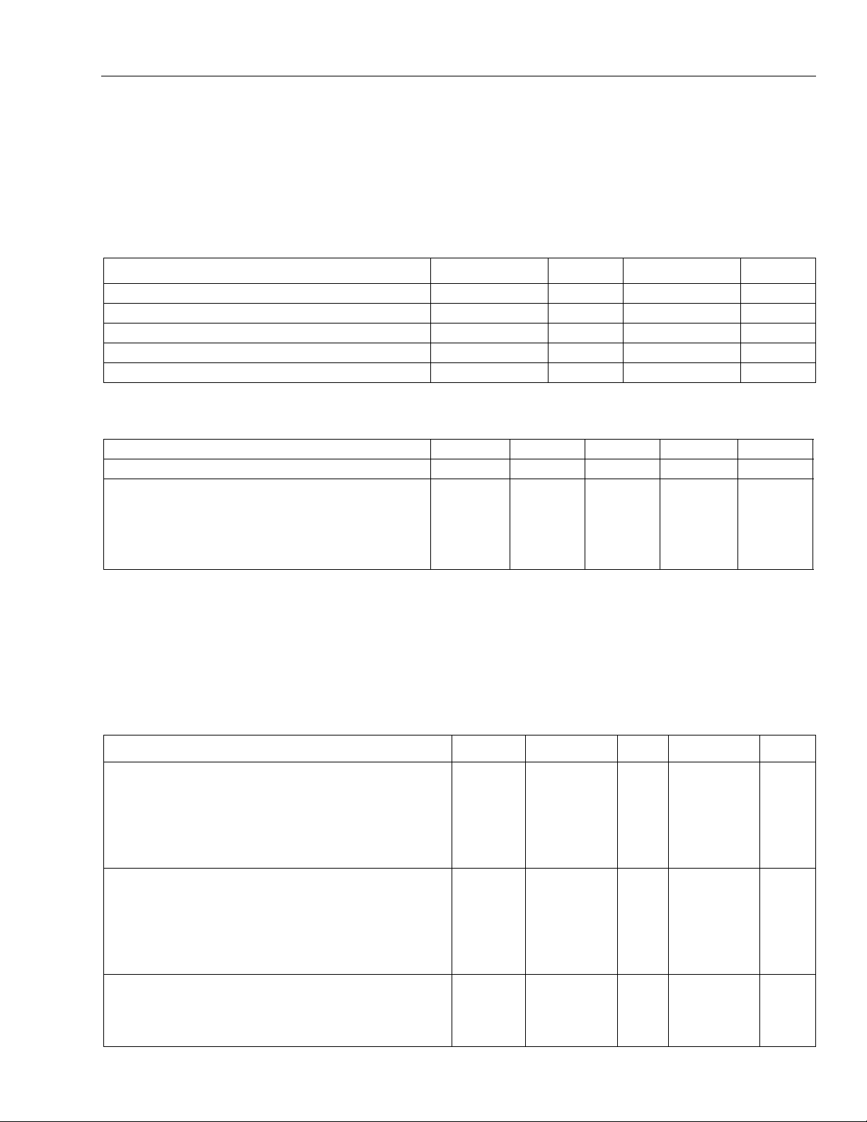
Data Sheet LU3X54FTL
July 2000 QUAD-FET for 10Base-T/100Base-TX/FX
Absolute Maximum Ratings
(TA = 25 °C)
Stresses in excess of the absolute maximum ratings can cause permanent damage to the device. These are absolute stress ratings only. Functional operation of the device is not implied at these or any other conditions in excess
of those given in the operational sections of the data sheet. Exposure to absolute maximum ratings for extended
periods can adversely affect device reliability.
Table 25. Absolute Maximum Ratings
Parameter Symbol Min Max Unit
Ambient Operating Temperature T
Storage Temperature T
Power Dissipation P
A
stg
D
Voltage on Any Pin with Respect to Ground — –0.5 V
070°C
–40 125 °C
—3.5W
DD
+ 0.5 V
Maximum Supply Voltage — — 5.5 V
Table 26. Operating Conditions
Parameter Symbol Min Typ
*
Max Unit
Operating Supply Voltage — 4.75 5.0 5.25 V
Power Dissipation:
All Ports 100 Mbits/s TX
All Ports 100 Mbits/s FX
All Ports 10 Mbits/s
All Ports Autonegotiating
D
P
D
P
D
P
D
P
—
—
—
—
3.0
2.2
2.0
1.5
—
—
—
—
W
W
W
W
* Typical power dissipations are specified at 5.0 V and 25 °C. This is the power dissipated by the LU3X54FTL. An additional 0.2 W of power is
required for the external twisted-pair driver termination resistors.
Electrical Characteristics
The following specifications apply for VDD = 5 V ± 5%, V
Table 27. dc Characteristics
Parameter Symbol Min Typ Max Unit
TTL Inputs: V
DD3
= 3.3 V ± 5%
Input High Voltage
Input Low Voltage
Input High Current
Input Low Current
Input Leakage Current
CMOS Inputs: V
DD3
= 5.0 V ± 5%
Input High Voltage
Input Low Voltage
Input High Current
Input Low Current
Input Leakage Current
TTL Outputs: V
DD3
= 3.3 V ± 5% or V
DD3
= 5.0 V ± 5%
Output High Voltage
Output Low Voltage
Output Shor t -cir cui t Current
DD3
= 5 V ± 5% or V
IH
V
IL
V
IH
I
IL
I
L
I
IH
V
IL
V
IH
I
IL
I
L
I
OH
V
OL
V
SC
I
DD3
= 3.3 V ± 5%.
2.0
—
—
—
—
3.0
—
—
—
—
2.4
—
–4
—
—
—
—
—
—
—
—
—
—
—
—
—
—
0.8
50
–400
50
—
0.5
1
–1
1
—
0.45
–85
V
V
µA
µA
µA
V
V
µA
µA
µA
V
V
mA
Lucent Technologies Inc. 41

LU3X54FTL Data Sheet
QUAD-FET for 10Base-T/100Base-TX/FX July 2000
Electrical Characteristics
Table 27. dc Characteristics
(continued)
(continued)
Parameter Symbol Min Typ Max Unit
10 Mbits/s Twisted Pair: Input Voltage V
100 Mbits/s Twisted Pair: Input Voltage V
10 Mbits/s Twisted Pair: Output Current V
100 Mbits/s Twisted Pair: Output Current V
DIFF
DIFF
DIFF
DIFF
0.35 — 2.0 V
——1.5V
45 50 55 mA
19 20 21 mA
Timing Characteristics (Preliminary)
Table 28. MII Management Interface Timing (25 pF Load)
Name Parameter Min Typ Max Unit
t1 MDIO Valid to Rising Edge of MDC (setup) 10 — — ns
t2 Rising Edge of MDC to MDIO Invalid (hold) 10 — — ns
t3 MDC Falling Edge to MDIO Valid (prop. delay) 0 — 40 ns
t4 MDC High* — 200 — ns
t5 MDC Low* 40 200 — ns
t6 MDC Period* 80 400 — ns
* When operating MDC above 6.25 MHz, MDC must be synchronous with LSCLK and have a setup time of 15 ns and a hold time of 5 ns,
with respect to LSCLK.
MDC
MDIO
MDIO
t1
Figure 9. MDIO Input Timing
MDC
t5 t4
t3
Figure 10. MDIO Output Timing
t2
t6
5-4959(F).r1
5-4960(F).c
42 Lucent Technologies Inc.

Data Sheet LU3X54FTL
July 2000 QUAD-FET for 10Base-T/100Base-TX/FX
Timing Characteristics (Preliminary)
< R > < Z > < O >
MDC
MDIO
Note: MDIO turnaround (TA) time is a 2-bit time spacing between the register address field, and the data field of a frame to avoid drive conten-
tion on MDIO during a read transaction. During a write to the LU3X54FTL, these bits are driven to a 10 by the station. During a read, the
MDIO is not driven during the first bit time and is driven to a 0 by the LU3X54FTL during the second bit time.
(continued)
5-5312(F)
Figure 11. MDIO During TA (Turnaround) of a Read Transaction
Table 29. MII Data Timing (25 pF Load)
Name Parameter Min Typ Max Unit
t1 RXD[3:0], RX_ER, RX_DV Valid to RX_CLK High 10/100 — — ns
t2 RX_CLK High to RXD[3:0], RX_DV, RX_ER Invalid 10/100 — — ns
t3 RX_CLK High 14/180 — 26/220 ns
t4 RX_CLK Low 14/180 — 26/220 ns
t5 RX_CLK Period — 40 — ns
t6 TX_CLK High 14/180 — 26/220 ns
t7 TX_CLK Low 14/180 — 26/220 ns
t8 TX_CLK Period — 40 — ns
t9 TXD, TX_EN, TX_ER, Setup to TX_CLK 18/140 — — ns
t10 TXD, TX_EN, TX_ER, Hold to TX_CLK 0/0 — — ns
t11 TXD, TX_EN, TX_ER, Setup to LSCLK* 12 — — ns
t12 TXD, TX_EN, TX_ER, Hold to LSCLK* 0 — — ns
t13 TX_CLK Skew from LSCLK TBD — TBD ns
t14 First Bit of J on TPIN± While Transmitting Data to COL
— — 170 ns
Assert (half-duplex mode)
t15 First Bit of T Received on TPIN± While Transmitting to COL
— — 210 ns
Deasserted (half-duplex mode)
* 100 Mbits/s only.
Lucent Technologies Inc. 43

LU3X54FTL Data Sheet
QUAD-FET for 10Base-T/100Base-TX/FX July 2000
Timing Characteristics (Preliminary)
RX_CLK
RXD[3:0]
RX_DV
RX_ER
t1
TX_CLK
TXD[3:0]
TX_EN
TX_ER
LSCLK
(continued)
t5
t3t4
t2
t8
t7
t9
t6
t10
TXD[3:0]
TX_EN
TX_ER
LSCLK
TX_CLK
TPIN
COL
t13
±
1st BIT OF J
t14
t11
t12
1st BIT OF T
t15
Figure 12. MII Timing Requirements for LU3X54FTL
5-5432(F).r2
44 Lucent Technologies Inc.
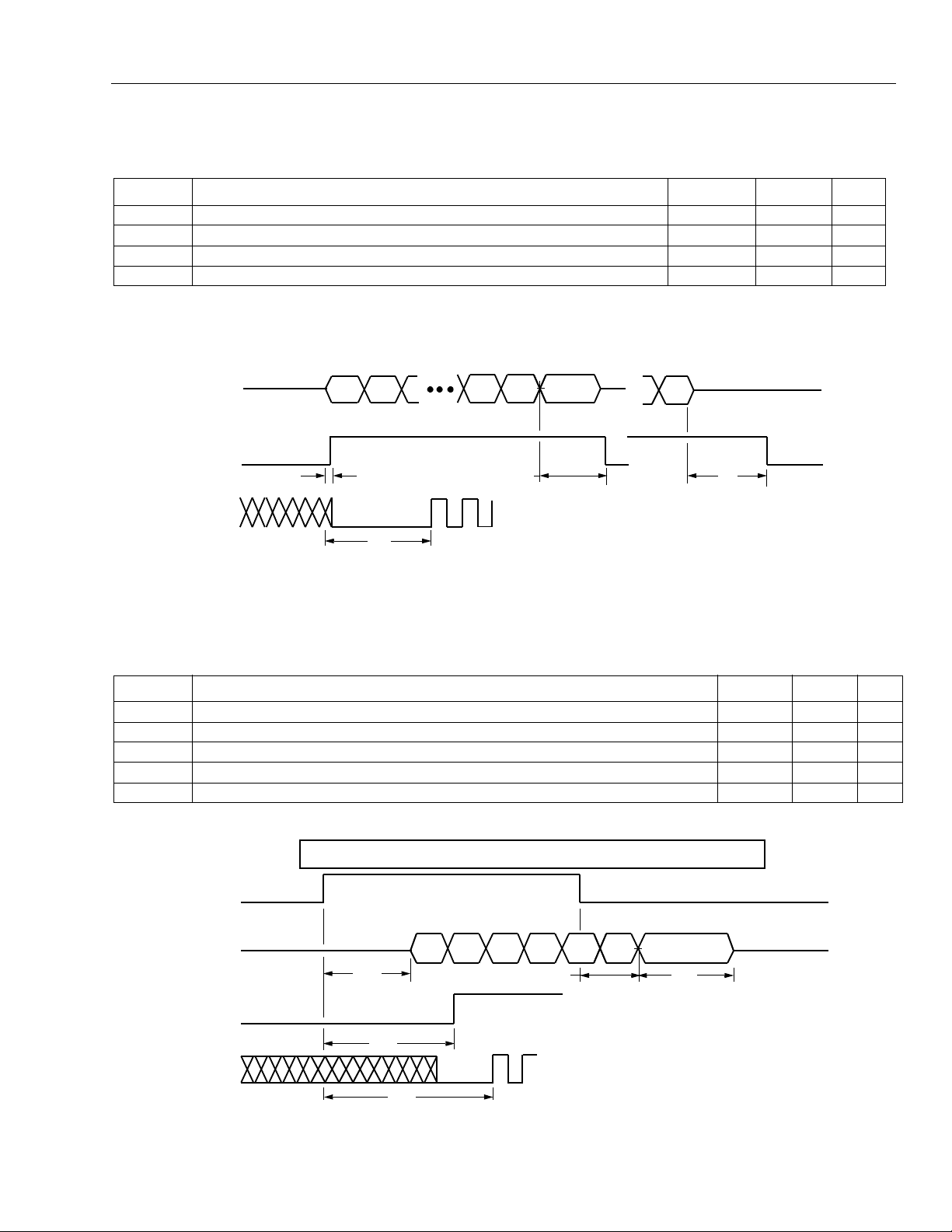
Data Sheet LU3X54FTL
July 2000 QUAD-FET for 10Base-T/100Base-TX/FX
Timing Characteristics (Preliminary)
(continued)
Table 30. Serial 10 Mbits/s Timing for TPIN, CRS, and RX_CLK
Name Parameter Min Max Unit
t16 TPIN Activity to CRS Assertion 40 500 ns
t17 TPIN Activity to RX_CLK Valid 800 2300 ns
t18 IDL to CRS Deassertion 200 550 ns
t19 Dead Signal to CRS Deassertion 400 1000 ns
(RECEIVE—DEAD SIGNAL)
(NOT IDL)
(RECEIVE—START OF PACKET) (RECEIVE—END OF PACKET)
TPIN
±
CRS
t16 t18
RX_CLK
t17
IDL
t19
5-5293(F).cr3
Figure 13. Serial 10 Mbits/s Timing for TPIN, CRS, and RX_CLK
Table 31. Serial 10 Mbits/s Timing for TX_EN, TPOUT, CRS, and RX_CLK
Name Parameter Min Max Unit
t20 TX_EN Asserted to Transmit Pair Activity 50 400 ns
t21 TX_EN Asserted to CRS Asserted Due to Internal Loopback 5 1900 ns
t22 TX_EN Asserted to RX_CLK Valid Due to Internal Loopback 1000 1700 ns
t23 TX_EN Deasserted to IDL Transmission 50 300 ns
t24 IDL Pulse Width 250 350 ns
(TRANSMIT—START OF PACKET) (TRANSMIT—END OF PACKET)
TX_EN
TPOUT
CRS
RX_CLK
±
t20
t21
t23
IDL
t24
t22
5-5293(F).dr3
Figure 14. Serial 10 Mbits/s Timing for TX_EN, TPOUT, CRS, and RX_CLK
Lucent Technologies Inc. 45
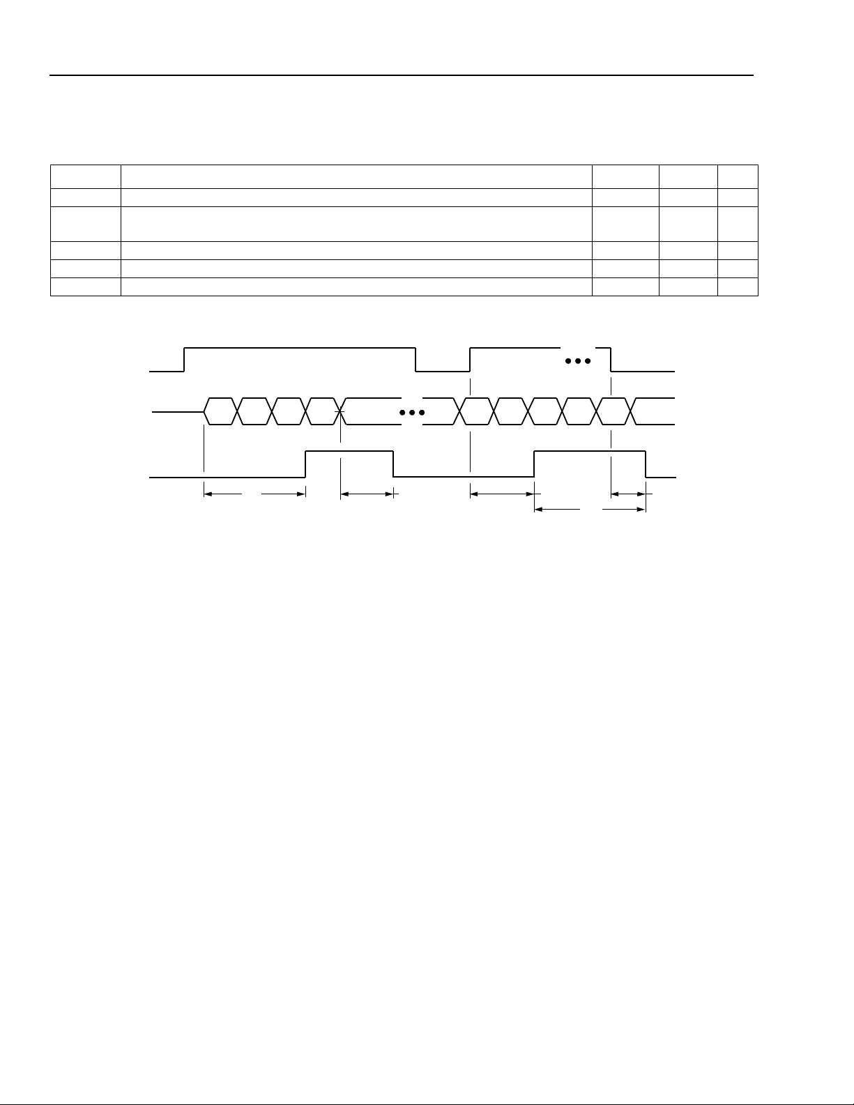
LU3X54FTL Data Sheet
QUAD-FET for 10Base-T/100Base-TX/FX July 2000
Timing Characteristics (Preliminary)
(continued)
Table 32. Serial 10 Mbits/s Timing for TX_EN, TPIN, and COL
Name Parameter Min Max Unit
t25 Time to Assert COL; LU3X54FTL Is Transmitting; Receive Activity Starts 40 400 ns
t26 Time to Deassert COL; LU3X54FTL Is Transmitting; Receive Activity
300 900 ns
Ceases
t27 Time to Assert COL; LU3X54FTL Is Receiving; Transmit Activity Starts 5 400 ns
t28 Time to Deassert COL; LU3X54FTL Is Receiving; Transmit Activity Ceases 5 900 ns
t29 COL Pulse Width 100 — ns
(TRANSMITTING—RECEIVE COLLISION DETECTED) (RECEIVING—TRANSMIT COLLISON DETECTED)
TX_EN
TPIN
±
COL
t25 t26 t27 t28
IDL
t29
Figure 15. Serial 10 Mbits/s Timing for TX_EN, TPIN, and COL
5-5293(F).er3
46 Lucent Technologies Inc.
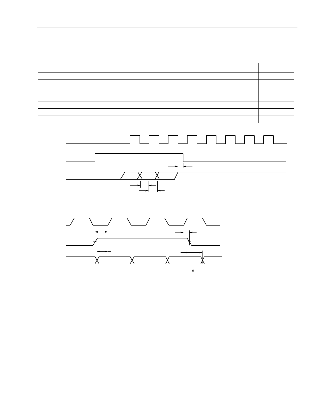
Data Sheet LU3X54FTL
July 2000 QUAD-FET for 10Base-T/100Base-TX/FX
Timing Characteristics (Preliminary)
(continued)
Table 33. Serial 10 Mbits/s Timing for RX_CLK, CRS, RXD, TX_CLK, TX_EN, and TXD (25 pF Load)
Name Parameter Min Max Unit
t30 RXD Setup Before RX_CLK Rising Edge 30 — ns
t31 RXD Held Past RX_CLK Edge 30 — ns
t32 RX_CLK Low to CRS Deassertion (at end of received packet) 40 — ns
t33 TX_EN Setup Before TX_CLK Rising Edge 30 — ns
t34 TX_EN Held Past TX_CLK Rising Edge 0 — ns
t35 TXD Setup Before TX_CLK Rising Edge 30 — ns
t36 TXD Held Past TX_CLK Rising Edge 0 — ns
RX_CLK
CRS
t32
RXD
t30
(START OF PACKET) (END OF PACKET)
t31
TX_CLK
t33
TX_EN
t35
TXD
t34
t36
LAST BIT
Figure 16. Serial 10 Mbits/s Timing for RX_CLK, CRS, RXD, TX_CLK, TX_EN, and TXD
5-2736(C).b
Lucent Technologies Inc. 47
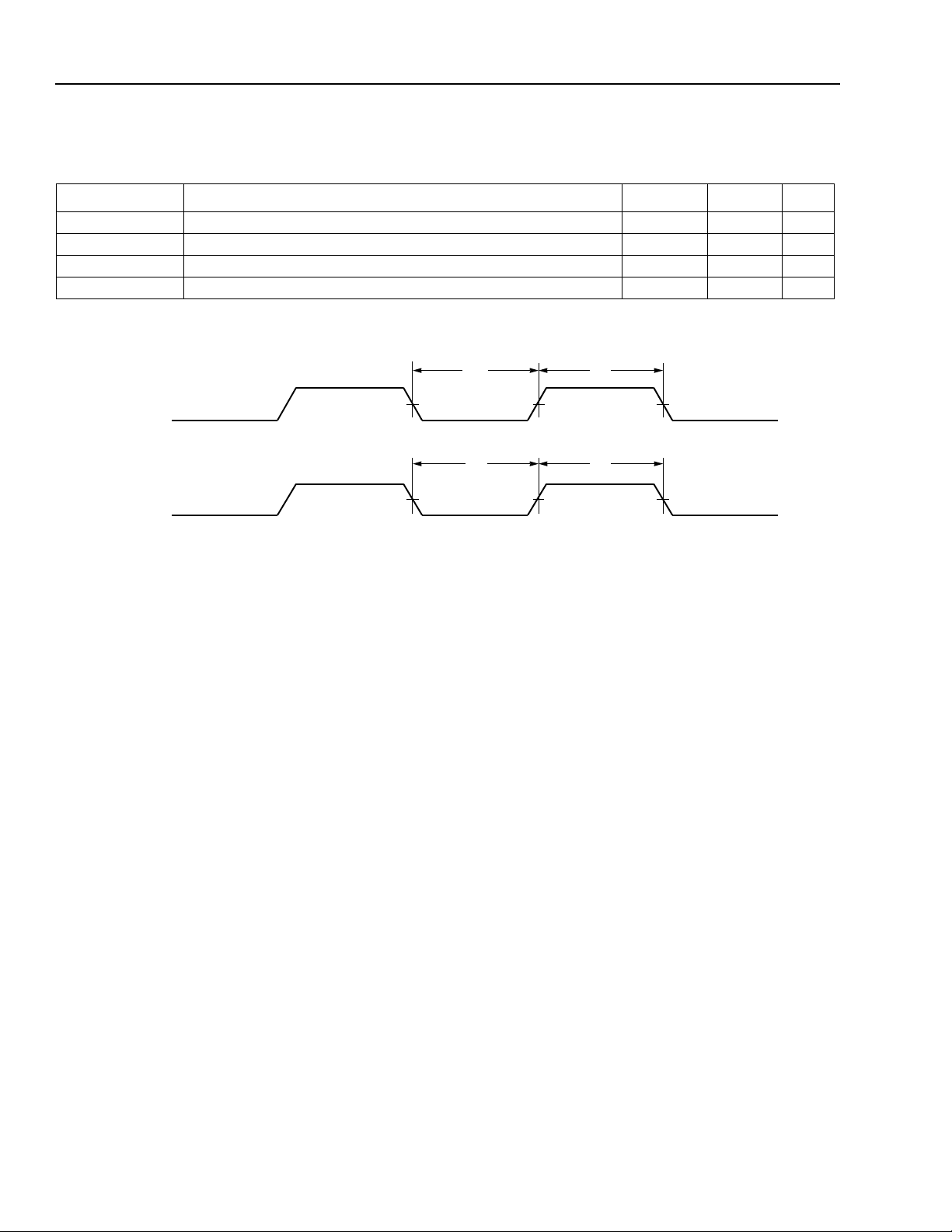
LU3X54FTL Data Sheet
QUAD-FET for 10Base-T/100Base-TX/FX July 2000
Timing Characteristics (Preliminary)
(continued)
Table 34. Serial 10 Mbits/s Timing for RX_CLK and TX_CLK (25 pF Load)
Name Parameter Min Max Unit
t37 RX_CLK Low Pulse Width 45 55 ns
t38 RX_CLK High Pulse Width 45 55 ns
t39 TX_CLK Low Pulse Width 45 55 ns
t40 TX_CLK High Pulse Width 45 55 ns
t37 t38
RX_CLK
t40t39
TX_CLK
Figure 17. Serial 10 Mbits/s Timing Diagram for RX_CLK and TX_CLK
5-2737(F).br3
48 Lucent Technologies Inc.

Data Sheet LU3X54FTL
July 2000 QUAD-FET for 10Base-T/100Base-TX/FX
Timing Characteristics (Preliminary)
(continued)
Table 35. 100 Mbits/s MII T ransmit Timing
Name Parameter Min Max Unit
t41 Rising Edge of TX_CLK Following TX_EN Assertion to CRS Assertion — 40 ns
t42 Rising Edge of TX_CLK Following TX_EN Assertion to TPOUT± —60ns
t43 Rising Edge of TX_CLK Following TX_EN Deassertion to CRS Deassertion — 40 ns
TX_CLK
TX_EN
TXD[3:0]
t43
5-3745(F).br4
CRS
TPOUT
t41
1st BIT OF J 1st BIT OF T
t42
±
Figure 18. 100 Mbits/s MII Transmit Timing
Lucent Technologies Inc. 49

LU3X54FTL Data Sheet
QUAD-FET for 10Base-T/100Base-TX/FX July 2000
Timing Characteristics (Preliminary)
(continued)
Table 36. 100 Mbits/s MII Receive Timing
Name Parameter Min Max Unit
t44 TPIN± 1st Bit of J Receive Activity to CRS Asserted — 170 ns
t45 TPIN± Receive Activity to Receive Data Valid — 210 ns
t46 TPIN± Receive Activity Cease (1st bit of T) to CRS Deasserted — 210 ns
t47 TPIN± Receive Activity Cease (1st bit of T) to Receive Data Not Valid — 210 ns
1st BIT OF J 1st BIT OF T
±
TPIN
t44
CRS
RX_CLK
t45
RX_DV
RX_ER
t46
t47
RXD[3:0]
5-3747(F).br4
Figure 19. 100 Mbits/s MII Receive Timing
50 Lucent Technologies Inc.

Data Sheet LU3X54FTL
July 2000 QUAD-FET for 10Base-T/100Base-TX/FX
Outline Diagram
208-Pin SQFP
Dimensions are in millimeters.
30.60 ± 0.20
28.00 ± 0.20
PIN #1 IDENTIFIER ZONE
157208
1.30 REF
1
52
53 104
DETAIL BDETAIL A
156
28.00
± 0.20
105
3.40 ± 0.20
SEATING PLANE
30.60
± 0.20
GAGE PLANE
0.17/0.27
0.25
DETAIL A
DETAIL B
0.090/0.200
0.10
0.50/0.75
M
4.10 MAX
SEATING PLANE
0.50 TYP
0.25 MIN
0.08
5-2196(F).r13
Lucent Technologies Inc. 51

LU3X54FTL Data Sheet
QUAD-FET for 10Base-T/100Base-TX/FX July 2000
Ordering Information
Device Code Comcode Package Temperature
LU3X54FTL-HS208-DB
108420167
208-Pin SQFPH (Heat Spreader)
0 °C to 70 °C
For additional information, contact your Microelectronics Group Account Manager or the following:
INTERNET:
E-MAIL:
N. AMERICA: Microelectronics Group, Lucent Technolog ie s Inc., 555 U nion Boulevard, Room 30L-15P-BA, Allentown, PA 18109-3286
ASIA PACIFIC: Microelectro ni cs Gro up, Lucent Technologies Singapore Pte. Ltd., 77 Science Park Drive, #03-18 Cintech III, Singapore 118256
CHINA: Microelectronics Group, Lucent Technologies (China) Co., Ltd., A-F2, 23/F, Zao Fong Universe Building, 1800 Zhong Shan Xi Road,
JAPAN: Microelectronics Group, Lucent Technologies Japan Ltd., 7-18, Higashi-Gotanda 2-chome, Shinagawa-ku, Tokyo 141, Japan
EUROPE: Data Requests: MICROELECTRONICS GROUP DATALINE:
Lucent Technologies Inc. reserves the right to make changes to the product(s) or information contained herein without notice. N o liability is assumed as a result of their use or application. No
rights under any patent accompany the sale of any such product(s) or information.
Copyright © 2000 Lucent Technologies Inc.
All Rights Reserved
Printed in U.S.A.
http://www.lucent.com/micro
docmaster@micro.lucent.com
1-800-372-2447
Tel. (65) 778 8833
Shanghai 200233 P. R. China
Tel. (81) 3 5421 1600
Technical Inq ui ries: GERMANY:
, FAX 610-712-4106 (In CANADA:
, FAX (65) 777 7495
, FAX (81) 3 5421 1700
FRANCE:
(39) 2 6608131
ITAL Y:
1-800-553-2448
Tel. (86) 21 6440 0468, ext. 325
(49) 89 95086 0
(33) 1 48 83 68 00
(Munich), UNITED KINGDOM:
(Paris), SWEDEN:
(Milan), SPAIN:
(34) 1 807 1441
, FAX 610-712-4106)
, F A X ( 86) 21 6440 0652
Tel. (44) 1189 324 299
(44) 1344 865 900
(46) 8 600 7070
(Madrid)
, FAX (44) 1189 328 148
(Bracknell),
(Stockhol m), F I NLAN D:
(358) 9 4354 28 00
(Helsinki),
July 2000
DS00-354LAN (Replaces DS98-277LAN)
 Loading...