

AGERE LU3X34FTR-HS128-DB Datasheet

Preliminary Data Sheet
July 2000
Quad 3 V 10/100 Ethernet Transceiver TX/FX
Overview
The LU3X34FTR is a fully integrated, 4-port
10/100 Mbits/s physical layer device with an integrated transceiver. This part was designed specifically for 10/100 Mbits/s switches. These applications
typically require stringent functionality in addition to
very tight board space, power, and cost requirements. The LU3X34FTR supports RMII and SMII
interfaces, offering the designer multiple reduced pin
count interfaces to save both real estate and cost in
system design. The LU3X34FTR was designed from
the beginning to conform fully with all pertinent specifications, from the
568 cabling guidelines to
5
IEEE
802.3 Ethernet specifications.
ISO
1
/
2
IEC
11801 and
ANSI
3
EIA
4
X3.263TP-PMD to
/TIA
LU3X34FTR
■
FX mode configurable on a per-port basis.
■
Built-in analog 10 Mbit receive filter, removing the
need for external filters.
■
Built-in 10 bit transmit filter.
■
10 Mbit PLL, exceeding tolerances for both
preamble and data jitter.
■
100 Mbit PLL, combined with the digital adaptive
equalizer, robustly handles variations in rise-fall
time, excessive attenuation due to channel loss,
duty-cycle distortion, crosstalk, and baseline
wander.
■
Transmit rise-fall time manipulated to provide lower
emissions, amplitude fully compatible for proper
interoperability.
Features
■
4-port, single-chip, integrated physical layer and
transceivers for 10Base-T, 100Base-TX, or
100Base-FX functions.
■
IEEE
802.3 compatible 10Base-T and 100Base-T
physical layer interface and ANSI X3.263 TP-PMD
compatible transceiver.
■
Interface support for RMII and SMII switch
applications.
■
Autonegotiation pin configurability on a per-port
basis.
1.
ISO
is a registered trademark of The International Organization
of Standardization.
2.
IEC
is a registered trademark of The International Electrotechni-
cal Commission.
3.
EIA
is a registered trademark of Electronic Industries Associa-
tion.
ANSI
is a registered trademark of American National Standards
4.
Institute, Inc.
5.
IEEE
is a registered trademark of The Institute of Electrical and
Electronics Engineers, Inc.
■
Programmable scrambler seed for better FCC
compliancy.
■
IEEE
802.3u Clause 28 compliant autonegotiation
for full 10 Mbits/s and 100 Mbits/s control.
■
Extended management support with interrupt
capabilities.
■
PHY MIB support.
■
Low-power 500 mA max.
— Low-cost 128-pin SQFP packaging with heat
spreader.

LU3X34FTR Preliminary Data Sheet
Quad 3 V 10/100 Ethernet Transceiver TX/FX July 2000
Table of Contents
Contents Page
Overview................................................................................................................................................................... 1
Features ................................................................................................................................................................... 1
Description................................................................................................................................................................ 4
Pin Information ......................................................................................................................................................... 5
Pin Descriptions........................................................................................................................................................ 7
Functional Description............................................................................................................................................ 13
Reduced Media Independent Interface (RMII) .................................................................................................... 13
Serial Media Independent Interface (SMII).......................................................................................................... 15
Media Independent Interface (MII)—Internal....................................................................................................... 17
100Base-X Module.............................................................................................................................................. 19
Scrambler Block .................................................................................................................................................. 22
100Base-TX Transceiver..................................................................................................................................... 24
10Base-T Module................................................................................................................................................ 25
Reset Operation.................................................................................................................................................. 28
MII Registers ............................................................. ...... ....... ........................................ ..... ...... ............................. 30
dc and ac Specifications......................................................................................................................................... 43
Absolute Maximum Ratings................................................................................................................................. 43
Clock Timing........................................................................................................................................................... 44
Outline Diagram...................................................................................................................................................... 50
128-Pin SQFP..................................................................................................................................................... 50
Ordering Information............................................................................................................................................... 51
Tables Page
Table 1. MII Interface Cross-Reference ................................................................................................................... 7
Table 2. Twisted-Pair Magnetic Interface ................................................................................................................. 8
Table 3. Twisted-Pair Transceiver Control/Transmitter Control................................................................................. 8
Table 4. MII Interface (RMII Mode) .......................................................................................................................... 8
Table 5. MII Interface (SMII Mode) .......................................................................................................................... 9
Table 6. LED/Configuration Pins............................................................................................................................ 10
Table 7. Special Mode Configurations ................................................................................................................... 11
Table 8. Clock and Chip Reset .............................................................................................................................. 12
Table 9. Power and Ground ................................................................................................................................... 12
Table 10. Receive Data/Status Encoding .............................................................................................................. 16
Table 11. Symbol Code Scrambler ........................................................................................................................ 21
Table 12. Autonegotiation ...................................................................................................................................... 29
Table 13. MII Management Registers.................................................................................................................... 30
Table 14. Control Register (Register 0h) ............................................................................................................... 30
Table 15. Status Register Bit Definitions (Register 1h).......................................................................................... 32
Table 16. PHY Identifier (Register 2h) ................................................................................................................... 34
Table 17. PHY Identifier (Register 3h) ................................................................................................................... 34
Table 18. Advertisement (Register 4h) .................................................................................................................. 35
Table 19. Autonegotiation Link Partner Ability (Register 5h) ................................................................................. 36
Table 20. Autonegotiation Expansion Register (Register 6h) ................................................................................ 36
Table 21. Programable LED (Register 11h)........................................................................................................... 37
Table 22. False Carrier Counter (Register 13h)..................................................................................................... 38
Table 23. Receive Error Counter (Register 15h).................................................................................................... 38
Table 24. PHY Control/Status Register (Register 17h).......................................................................................... 38
Table 25. Config 100 Register (Register 18h)........................................................................................................ 39
Table 26. PHY Address Register (Register 19h) ................................................................................................... 40
2 Lucent Technologies Inc.

Preliminary Data Sheet LU3X34FTR
July 2000 Quad 3 V 10/100 Ethernet Transceiver TX/FX
Table of Contents
(continued)
Tables Page
Table 27. Config 10 Register (Register 1Ah)..........................................................................................................41
Table 28. Status 100 Register (Register 1Bh)........................................................................................................41
Table 29. Status 10 Register (Register 1Ch)..........................................................................................................41
Table 30. Interrupt Mask Register (Register 1Dh)..................................................................................................42
Table 31. Interrupt Status Register (Register 1Eh).................................................................................................42
Table 32. Absolute Maximum Ratings....................................................................................................................43
Table 33. Operating Conditions..............................................................................................................................43
Table 34. dc Characteristics ...................................................................................................................................43
Table 35. Management Clock.................................................................................................................................44
Table 36. RMII Receive Timing...............................................................................................................................45
Table 37. RMII Transmit Timing..............................................................................................................................45
Table 38. Transmit Timing.......................................................................................................................................46
Table 39. Receive Timing.......................................................................................................................................46
Table 40. SMII Timing.............................................................................................................................................47
Table 41. Reset and Configuration Timing .............................................................................................................48
Table 42. PMD Characteristics...............................................................................................................................48
Figures Page
Figure 1. LU3X34FTR Block Diagram......................................................................................................................4
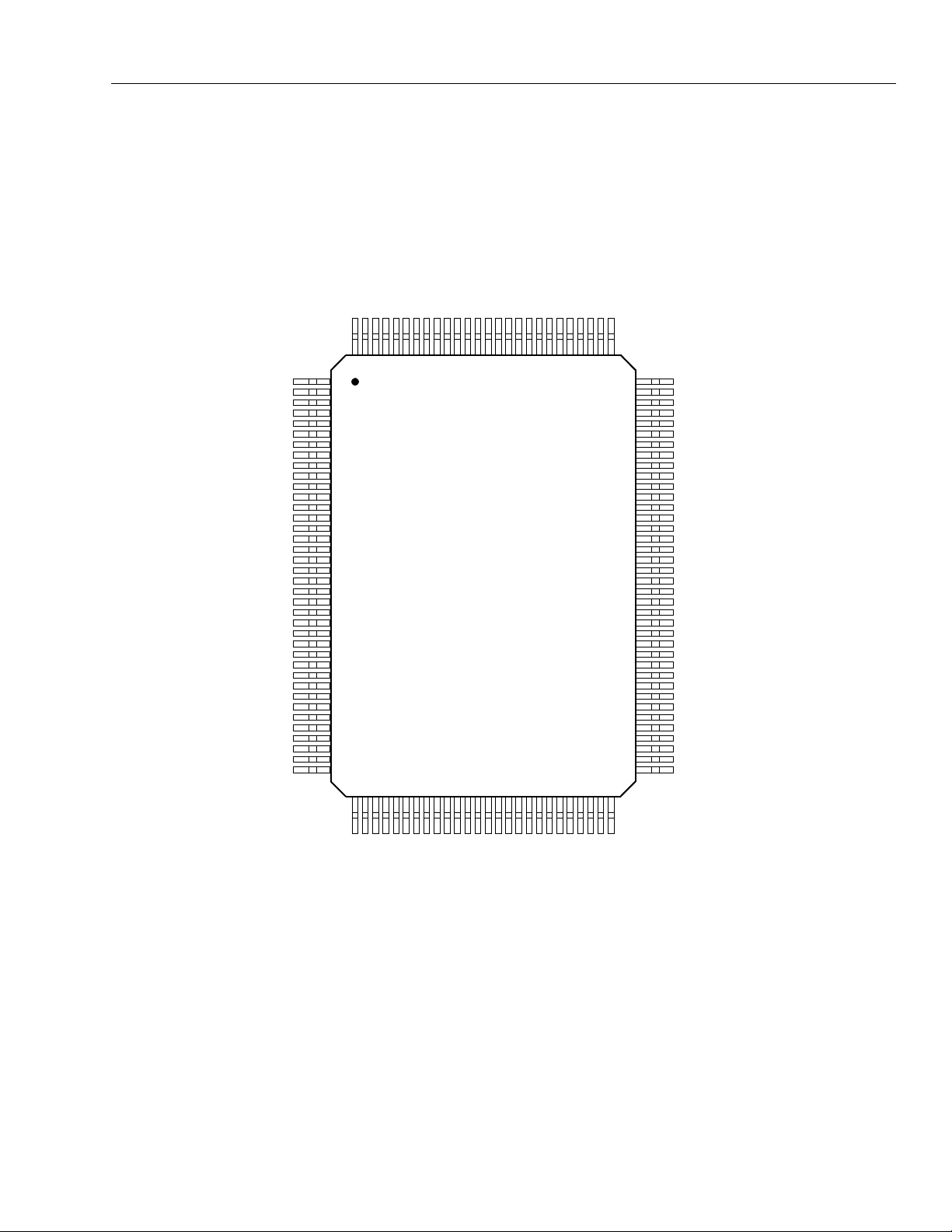
Figure 2. Pin Diagram (RMII Mode) .........................................................................................................................5
Figure 3. Pin Diagram (SMII Mode)..........................................................................................................................6
Figure 4. Functional Description ............................................................................................................................13
Figure 5. RMII Receive Timing from Internal MII Signals.......................................................................................14
Figure 6. SMII Connection Diagram.......................................................................................................................15
Figure 7. Receive Sequence Diagram ...................................................................................................................15
Figure 8. Transmit Sequence Diagram...................................................................................................................16
Figure 9. 100Base-X Data Path .............................................................................................................................19
Figure 10. 10Base-T Module Data Path.................................................................................................................25
Figure 11. LED Configuration.................................................................................................................................28
Figure 12. Management Clock...............................................................................................................................44
Figure 13. RMII Receive Timing.............................................................................................................................45
Figure 14. RMII Transmit Timing............................................................................................................................45
Figure 15. Transmit Timing.....................................................................................................................................46
Figure 16. Receive Timing .....................................................................................................................................46
Figure 17. SMII Timing...........................................................................................................................................47
Figure 18. Reset and Configuration Timing ...........................................................................................................48
Figure 19. PMD Characteristics .............................................................................................................................48
Figure 20. Connection Diagrams (Single-Channel 10/100BTX Operation)............................................................49
Lucent Technologies Inc. 3

LU3X34FTR Preliminary Data Sheet
Quad 3 V 10/100 Ethernet Transceiver TX/FX July 2000
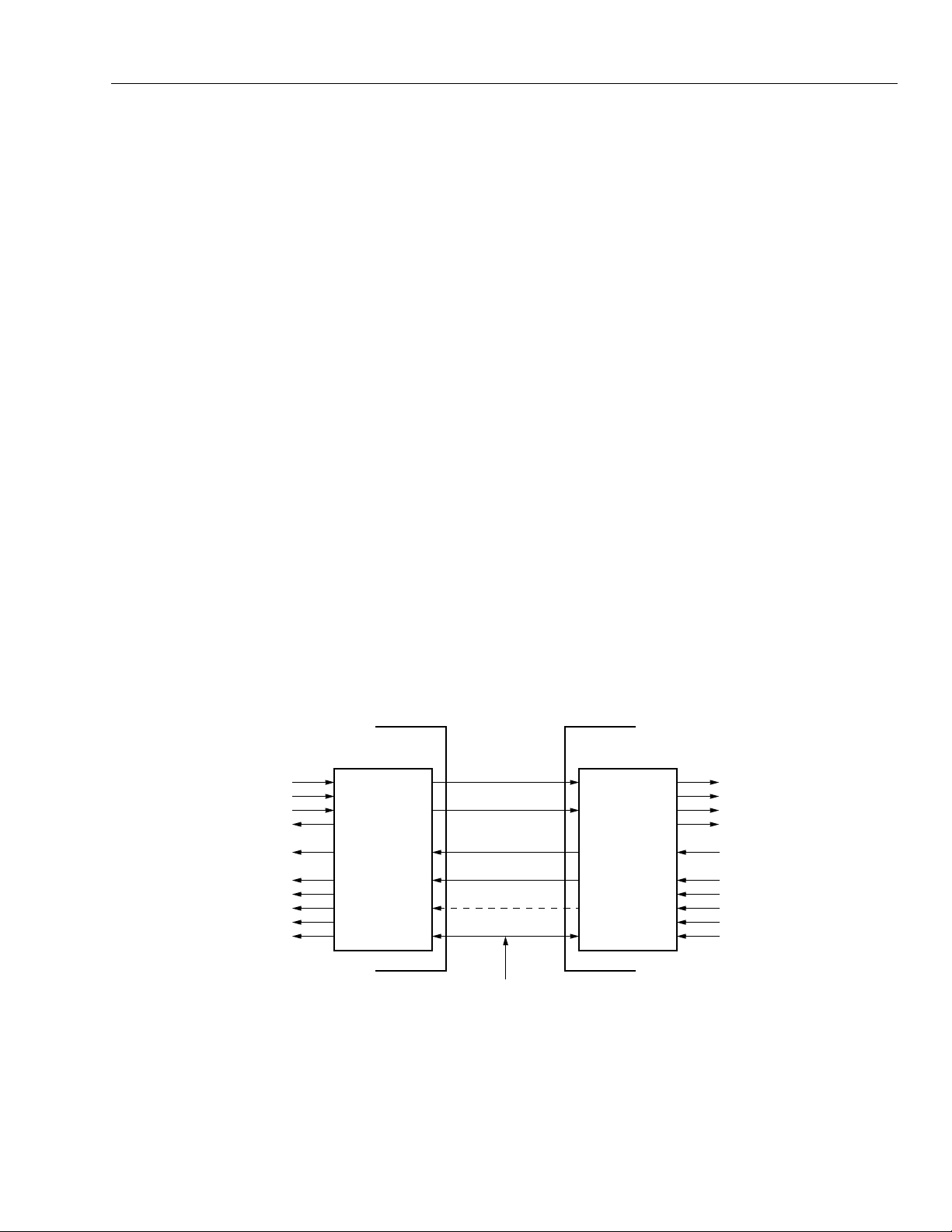
Description
INTZ
GLOBAL
INTERRUPT
REF_CLK
RX
TXD[1:0], TX_EN RXD[1:0], CRS_DV
RMII/SMII-TO-MII MII-TO-RMII/SMII
CONVERSION
100BASE-T 100BASE-X
PCS
10/100 CLOCK
RECOVERY
SQUELCH/SIG_
±
DETECT
BLW CORRECTION
ADAPTIVE EQ.
SYNTHESIS
AUTONEG/
LINK
CLOCK
CONVERSION
PCS
TRANSMIT
10/100
TX
±
LED
REGISTERS
PORTS[3:0]
LED OUTPUTS
MANAGE-
MENT
CONTROL
MDC MDIO
5-7520(F)
Figure 1. LU3X34FTR Block Diagram
4 Lucent Technologies Inc.
Preliminary Data Sheet LU3X34FTR
July 2000 Quad 3 V 10/100 Ethernet Transceiver TX/FX
Pin Information
TMVDD1
HSGND1
HSVDD1
SUBGND1
IOGND1
IOVDD1
RMII_RXD_0[1]
RMII_TXD_0[1]
RMII_TXD_0[0]
TXEN_0
REF_CLK
ANEN_0/SD+0/LEDSP100_0
HD10_0/SD–0/LEDFD_0
HD100_0/LEDACT_0
FOSEL_0/LEDLNK_0
LEDGND1
LEDVDD1
ANEN_1/SD+1/LEDSP100_1
HD10_1/SD–1/LEDFD_1
HD100_1/LEDACT_1
FOSEL_1/LEDLNK_1
TESTMSEL
RXVDD0
RX+_0
RX–_0
RXGND0
REF100_0
TX+_0
TX–_0
TXVDD0
TXVDD1
TX–_1
TX+_1
REF100_1
RXGND1
RX–_1
RX+_1
RXVDD1
REFGND
CSVDD10
CSGND10
CSGND100
CSVDD100
REF10
RXVDD2
RX+_2
RX–_2
RXGND2
REF100_2
TX+_2
TX–_2
TXVDD2
TXVDD3
TX–_3
TX+_3
REF100_3
RXGND3
RX–_3
RX+_3
RXVDD3
RSTZERRESERVED
115
116
117
118
119
120
121
122
123
124
125
126
127
128
1
2
3
4
5
6
7
8
9
10
11
12
13
14
15
16
17
18
19
20
21
22
23
24
25
26
27
28
29
30
31
32
33
34
35
36
37
38
39404142434445464748495051525354555657585960616263
LU3X34FTR
RMII_RXD_0[0]
103
105
106
107
108
109
110
111
112
113
114
104
102
101
100
99
98
97
96
95
94
93
92
91
90
89
88
87
86
85
84
83
82
81
80
79
78
77
76
75
74
73
72
71
70
69
68
67
66
65
64
RMII_RXER_0
CRS_DV_0
FD100_0/COL_0
TXEN_1
RMII_TXD_1[0]
RMII_TXD_1[1]
RMII_RXD_1[0]
RMII_RXD_1[1]
CRS_DV_1/PHYAD[2]
FD100_1/COL_1
DIGVDD1
DIGGND1
RMII_RXER_1
IOVDD3
IOGND3
RESERVED
RMII_RXER_2
FD10_3
DIGVDD2
DIGGND2
FD10_2
FD10_1
FD10_0
FD100_2/COL_2
CRS_DV_2/PHYAD[3]
RMII_RXD_2[1]
RMII_RXD_2[0]
RMII_TXD_2[1]
RMII_TXD_2[0]
TXEN_2
IOVDD4
IOGND4
RESERVED
RMII_RXER_3
FD100_3/COL_3
CRS_DV_3/PHYAD[4]
IOVDD5
RESERVED
INTZ
PAUSE
TPTXTR
ISOLATE
ANEN_2/SD+2/LEDSP100_2
LEDVDD2
LEDGND2
HD100_2/LEDACT_2
FOSEL_2/LEDLNK_2
HD10_2/SD–2/LEDFD_2
TXEN_3
HD100_3/LEDACT_3
FOSEL_3/LEDLNK_3
HD10_3/SD–3/LEDFD_3
ANEN_3/SD+3/LEDSP100_3
MDC
MDIO
RMII_TXD_3[0]
RMII_TXD_3[1]
RMII_RXD_3[0]
RMII_RXD_3[1]
HSVDD2
SUBGND2
IOGND5
HSGND2
TMGND1
5-7511(F).c.r7
Figure 2. Pin Diagram (RMII Mode)
Lucent Technologies Inc. 5
LU3X34FTR Preliminary Data Sheet
Quad 3 V 10/100 Ethernet Transceiver TX/FX July 2000
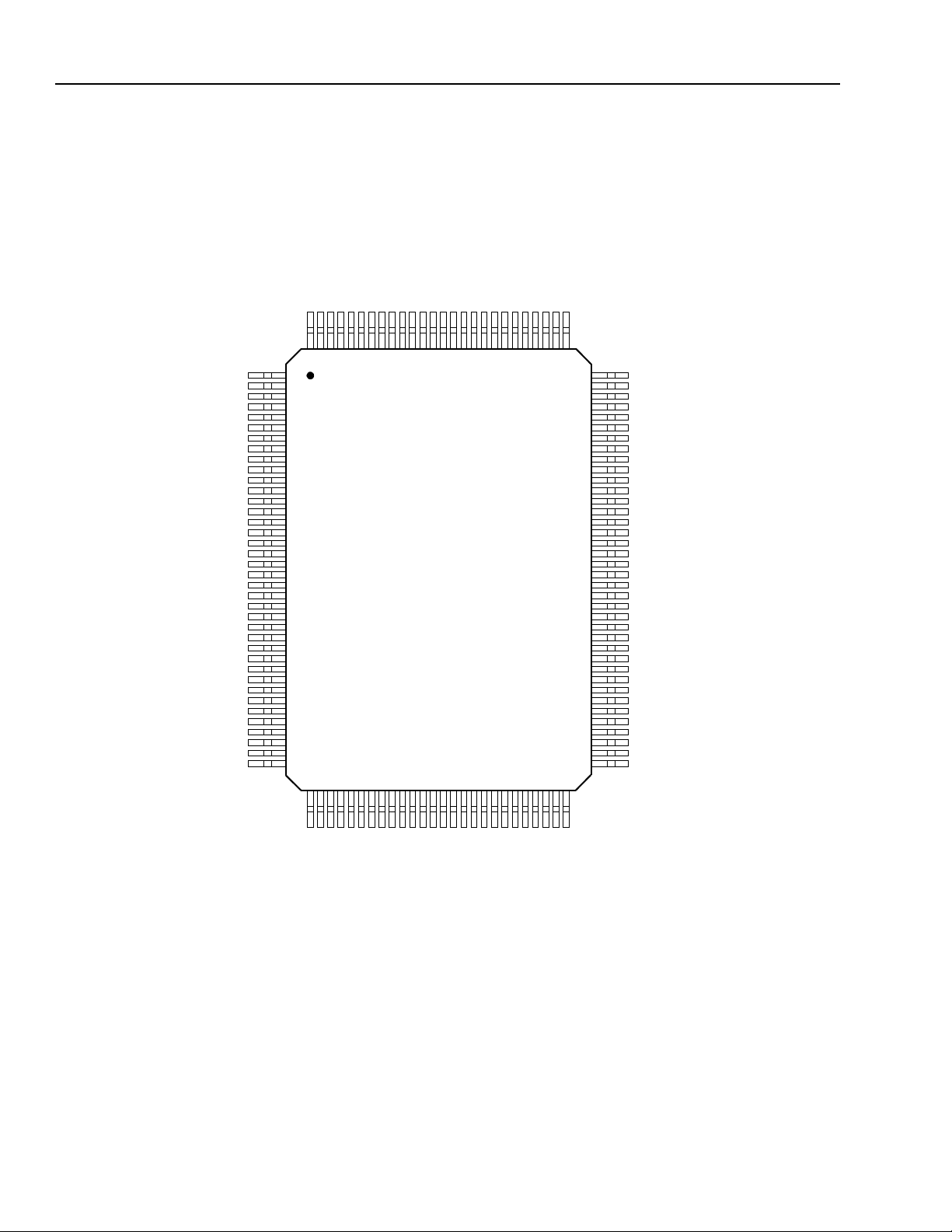
Pin Information
REF100_0
REF100_1
CSGND10
CSGND100
CSVDD100
REFF100_2
REFF100_3
(continued)
RXVDD0
RX+_0
RX–_0
RXGND0
TX+_0
TX–_0
TXVDD0
TXVDD1
TX–_1
TX+_1
RXGND1
RX–_1
RX+_1
RXVDD1
REFGND
CSVDD10
REF10
RXVDD2
RX+_2
RX–_2
RXGND2
TX+_2
TX–_2
TXVDD2
TXVDD3
TX–_3
TX+_3
RXGND3
RX–_3
RX+_3
RXVDD3
RSTZERRESERVED
122
123
124
125
126
127
128
1
2
3
4
5
6
7
8
9
10
11
12
13
14
15
16
17
18
19
20
21
22
23
24
25
26
27
28
29
30
31
32
33
34
35
36
37
38
39404142434445464748495051525354555657585960616263
121
120
HD100_0/LEDACT_0
116
117
118
119
LU3X34FTR
115
114
113
112
111
SMII_RXD_0
110
109
RESERVED
RESERVED
SMII_TXD_0
SMII_SYNC
REF_CLK
ANEN_0/SD+0/LEDSP100_0
HD10_0/SD–0/LEDFD_0
FOSEL_0/LEDLNK_0
LEDGND1
LEDVDD1
ANEN_1/SD+1/LEDSP100_1
HD10_1/SD–1/LEDFD_1
HD100_1/LEDACT_1
FOSEL_1/LEDLNK_1
TESTMSEL
IOGND1
IOVDD1
107
108
HSVDD1
SUBGND1
105
106
HSGND1
104
TMVDD1
103
102
101
100
64
RESERVED
SMII_EN
FD100_0/COL_0
99
98
97
96
95
94
93
92
91
90
89
88
87
86
85
84
83
82
81
80
79
78
77
76
75
74
73
72
71
70
69
68
67
66
65
RESERVED
SMII_TXD_1
RESERVED
SMII_RXD_1
RESERVED
PHYAD[2]
FD100_1/COL_1
DIGVDD1
DIGGND1
RESERVED
IOVDD3
IOGND3
RESERVED
RESERVED
FD10_3
DIGVDD2
DIGGND2
FD10_2
FD10_1
FD10_0
FD100_2/COL_2
PHYAD[3]
RESERVED
SMII_RXD_2
RESERVED
SMII_TXD_2
RESERVED
IOVDD4
IOGND4
RESERVED
RESERVED
FD100_3/COL_3
PHYAD[4]
IOVDD5
RESERVED
INTZ
PAUSE
TPTXTR
ISOLATE
ANEN_2/SD+2/LEDSP100_2
LEDVDD2
LEDGND2
HD100_2/LEDACT_2
FOSEL_2/LEDLNK_2
HD10_2/SD–2/LEDFD_2
RESERVED
HD100_3/LEDACT_3
FOSEL_3/LEDLNK_3
HD10_3/SD–3/LEDFD_3
ANEN_3/SD+3/LEDSP100_3
SMII_TXD_3
RESERVED
MDC
MDIO
RESERVED
SMII_RXD_3
IOGND5
HSVDD2
HSGND2
TMGND1
SUBGND2
5-7511(F).br6
Figure 3. Pin Diagram (SMII Mode)
6 Lucent Technologies Inc.

Preliminary Data Sheet LU3X34FTR
July 2000 Quad 3 V 10/100 Ethernet Transceiver TX/FX
Pin Descriptions
Table 1. MII Interface Cross-Reference
Pin
Number
RMII Mode SMII Mode
80 FD10_0 FD10_0
81 FD10_1 FD10_1
82 FD10_2 FD10_2
85 FD10_3 FD10_3
100 FD100_0/
93 FD100_1/
79 FD100_2/
68 FD100_3/
COL_0
COL_1
COL_2
COL_3
FD100_0
FD100_1
FD100_2
FD100_3
99 TXEN_1 RESERVED
73 TXEN_2 RESERVED
53 TXEN_3 RESERVED
113 TXEN_0 SMII_SYNC
102 RMII_RXER_0 RESERVED
112 RMII_TXD_0[0] SMII_TXD_0
111 RMII_TXD_0[1] RESERVED
110 RMII_RXD_0[0] SMII_RXD_0
109 RMII_RXD_0[1] RESERVED
101 CRS_DV_0 SMII_EN
98 RMII_TXD_1[0] SMII_TXD_1
97 RMII_TXD_1[1] RESERVED
96 RMII_RXD_1[0] SMII_RXD_1
95 RMII_RXD_1[1] RESERVED
86 RMII_RXER_2 RESERVED
94 CRS_DV_1/
78 CRS_DV_2/
PHYAD[2]
PHYAD[3]
PHYAD[2]
PHYAD[3]
90 RMII_RXER_1 RESERVED
67 CRS_DV_3/
PHYAD[4]
PHYAD[4]
54 RMII_TXD_3[0] SMII_TXD_3
55 RMII_TXD_3[1] RESERVED
56 RMII_RXD_3[0] SMII_RXD_3
57 RMII_RXD_3[1] RESERVED
69 RMII_RXER_3 RESERVED
74 RMII_TXD_2[0] SMII_TXD_2
75 RMII_TXD_2[1] RESERVED
76 RMII_RXD_2[0] SMII_RXD_2
77 RMII_RXD_2[1] RESERVED
59 MDIO MDIO
58 MDC MDC
87 RESERVED RESERVED
70 RESERVED RESERVED
65 RESERVED RESERVED
Lucent Technologies Inc. 7

LU3X34FTR Preliminary Data Sheet
Quad 3 V 10/100 Ethernet Transceiver TX/FX July 2000
Pin Descriptions
Table 2. Twisted-Pair Magnetic Interface
Pin No. Pin Name I/O Pin Description
6, 11, 28, 33
7, 10, 29, 32
3, 14, 25, 36
2, 15, 24, 37
Table 3. Twisted-Pair Transceiver Control/Transmitter Control
Pin No. Pin Name I/O Pin Description
5, 12, 27, 34 REF100_[0:3] I
22 REF10 I
127 ER I
41 TPTXTR I
(continued)
TX+_[0:3]
TX–_[0:3]
RX–_[0:3]
RX+_[0:3]
O
I
Transmit Driver Pairs
transmit 100Base-T MLT-3 signals across Category
5 UTP cable. 10Base-T Manchester signals acros s
Category 3, 4, or 5 UTP cable in twisted-pair operation or PECL data in fiber mode.
Receive Pair
data or 10Base-T Manchester data from the UTP
cable in twisted-pair mode or PECL data in fiber
mode.
Reference Pin for 100 Mbits/s Twisted-Pair
Driver
. The value of the connected resistor is 301 Ω.
Reference Pin for 10 Mbits/s Twisted-Pair Driver
The value for the connected resistor is 4.65 kΩ.
T ransmit Driver Edge Rate Control
the rise time of the transmit data will be less than
3.5 ns.
Network Interface 3-State Control
transmit drivers for the four ports are 3-stated.
. These pins receive 100Base-T MLT-3
. These pins are used to
.
. When set to 1,
. When high, the
Table 4. MII Interface (RMII Mode)
Pin No. Pin Name* I/O Pin Description
99, 73, 53 TXEN_[1:3] I
113 TXEN_0 I
102 RMII_RXER_0 I/O
112, 111 RMII_TXD_0[0:1] I
110, 109 RMII_RXD_0[0:1] I/O
101 CRS_DV_0/
98, 97 RMII_TXD_1[0:1] I/O
96, 95 RMII_RXD_1[0:1] O
94 CRS_DV_1/
SMII_EN
PHYAD[2]
I/O↓
I/O↓
Transmit Enable for Ports 1—3.
Transmit Enable for Port 0.
Receiver Error Output for Port 0.
illegal code-group has been received.
Transmit Data for Port 0.
Receive Data for Port 0.
CRS_DV Output for Port 0
input pin; logic level of 0 at this pin enables RMII
mode. This pin has an internal 40 kΩ pull-down
resistor that sets the MII interface to RMII mode without an external component. After reset, CRS_DV
output for port 0 is asserted only during receive
activity.
Transmit Data for Port 1.
Receive Data for Port 1.
CRS_DV Output for Port 1
input pin for PHY_address[2] configuration. This pin
has an internal 40 kΩ pull-down resistor that sets the
PHY_AD[2] to a 0 without an external component.
After reset, CRS_DV output for port 1 and is
asserted only during receive activity.
Indicates an
. During reset, this is an
. During reset, this is an
8 Lucent Technologies Inc.

Preliminary Data Sheet LU3X34FTR
July 2000 Quad 3 V 10/100 Ethernet Transceiver TX/FX
Pin Descriptions
Table 4. MII Interface (RMII Mode)
(continued)
(continued)
Pin No. Pin Name* I/O Pin Description
90 RMII_RXER_1 O
78 CRS_DV_2/
PHYAD[3]
I/O↓
Receiver Error Output for Port 1
CRS_DV Output for Port 2
input pin for PHY_address[3] configuration. This pin
has an internal 40 kΩ pull-down resistor that sets the
PHY_AD[3] to a 0 without an external component.
After reset, CRS_DV output for port 2 and is
asserted only during receive activity.
74, 75 RMII_TXD_2[0:1] I/O
76, 77 RMII_RXD_2[0: 1] O
86 RMII_RXER_2 O
67 CRS_DV_3/
PHYAD[4]
I/O↓
Transmit Data for Port 2
Receive Data for Port 2
Receiver Error for Port 2
CRS_DV Output for Port 3
input pin for PHY_address[4] configuration. This pin
has an internal 40 kΩ pull-down resistor that sets the
PHY_AD[4] to a 0 without an external component.
After reset, CRS_DV output for port 3 and is
asserted only during receive activity.
54, 55 RMII_TXD_3[0:1] I
56, 57 RMII_RXD_3[0: 1] I/O
69 RMII_RXER_3 O
59 MDIO I/O
58 MDC I
65, 87, 70 RESERVED O
* Smaller font indicates that the pin has multiple functions.
Transmit Data for Port 3
Receive Data for Port 3
Receive Error Output for Port 3
Management Data for Serial Register Access
Management Clock.
Reserved
. Leave this pin float.
Max clock rate = 2.5 MHz.
.
. During reset, this is an
.
.
.
. During reset, this is an
.
.
.
.
Table 5. MII Interface (SMII Mode)
Pin No. Pin Name* I/O Pin Description
113 SMII_SYNC I
112 SMII_TXD_0 I
110 SMII_RXD_0 I/O
101 SMII_EN I/O↓
SMII Sync Input.
Transmit Data for Port 0.
Receive Data for Port 0.
SMII_EN.
This pin must be pulled high at powerup or
reset to enable SMII mode. This input has an internal 40 kΩ pull-down resistor.
98 SMII_TXD_1 I/O
96 SMII_RXD_1 O
67, 78, 94 PHYAD[4:2] I/O
Transmit Data for Port 1.
Receive Data for Port 1.
Configure PHY Address
PHY_address 4 through 2 at powerup or reset. Each
of these pins has an internal 40 kΩ pull-down resistor that sets the corresponding PHY_AD to 0, without an external component.
54 SMII_TXD_3 I
56 SMII_RXD_3 I/O
74 SMII_TXD_2 I/O
76 SMII_RXD_2 O
59 MDIO I/O
Transmit Data for Port 3.
Receive Data for Port 3.
Transmit Data for Port 2.
Receive Data for Port 2.
Management Data for Serial Register Access
external resistive pull-up is needed on this pin.
. These pins configure
. An
Lucent Technologies Inc. 9

LU3X34FTR Preliminary Data Sheet
Quad 3 V 10/100 Ethernet Transceiver TX/FX July 2000
Pin Descriptions
Table 5. MII Interface (SMII Mode)
Pin No. Pin Name* I/O Pin Description
58 MDC I
53, 55, 73, 75,
97, 99, 111
57, 69, 77, 86,
90, 95, 102,
109
* Smaller font indicates that the pin has multiple functions.
Table 6. LED/Configuration Pins
Pin No. Pin Name I/O Pin Description
80, 81, 82, 85 FD10_[0:3] I
100, 93, 79,
68
(continued)
(continued)
RESERVED I
RESERVED 0
FD100_[0:3]/
COL_[0:3]
I↑
Management Clock.
Reserved.
Reserved.
Full-Duplex 10 Mbits/s
reset to configure the ports to 10 Mbits/s full-duplex
mode if autonegotiation is disabled. These pins will
set bit [6] in register 4h, the autonegotiation ability
register.
Full-Duplex 100 Mbits/s.
are latched at reset to configure the ports to
100 Mbits/s full-duplex mode if autonegotiation is
disabled. These pins will set bit [8] in register 4h, the
autonegotiation ability register. These inputs have
internal 40 kΩ pull-up resistors.
Tie to ground.
Let this pin float.
Max clock rate = 2.5 MHz.
. These pins are latched at
In switch mode, these pins
115, 121, 43, 49LEDSP100_ [0:3]/
ANEN_[0:3]/
SD+[0:3]
I/O↑
Collision Status Output
duplex mode when transmit and receive activities
are active simultaneously.
Speed LED Output
LED outputs indicate 100 Mbits/s line speed for
ports 0—3.
Autonegotiation Enable
logic low during reset, these are input pins to configure ports 0—3 to enable autonegotiation and sets bit
12 in register 0h.
Signal Detect +
detect + inputs.
These pins have an internal 40 kΩ pull-up resistor.
. In fiber mode, these pins are signal
. It is asserted during half-
. In twisted-pair mode, these
. If the FOSEL pin detects
10 Lucent Technologies Inc.

Preliminary Data Sheet LU3X34FTR
July 2000 Quad 3 V 10/100 Ethernet Transceiver TX/FX
Pin Descriptions
Table 6. LED/Configuration Pins
Pin No. Pin Name I/O Pin Description
116, 122, 44,
50
117, 123, 45, 51LEDCOL_ [0:3]/
40 PAUSE I
(continued)
LEDFD_[0:3]/
HD10_[0:3]/
SD–[0:3]
HD100_[0:3]
(continued)
I/O↑
I/O↑
Full-Duplex LED Output
por ts 0—3.
10 Mbits/s Half-Duplex Operation
during powerup or reset, these are input pins that
configure ports 0—3 for 10 Mbits/s half-duplex operation and sets register 4, bit 5 (see Figure 12). When
autonegotiation is disabled, it sets register 0, bit 13,
the speed bit, to 0 and bit 8, the duplex mode bit, to
0. If fiber mode is selected, bit 5, register 4h will be
set to 0.
Signal Detect –
negative signal detect input from the fiber module.
These pins have an internal 40 kΩ pull-up resistor.
Activity LED Outputs
status of ports 0—3, respectively.
100 Mbit/s Half-Duplex Operation.
or reset, these are input pins to configure ports 0—3
for 100 Mbits/s half-duplex operation and sets register 4, bit 7 (see Figure 12). If autonegotiation is disabled, it sets bit 13 in register 0 to 1. These pins
have an internal 40kΩ pull-up resistor.
Pause
. The logic level of this pin is latched into register 4, bit 10 for all four ports during powerup or
reset. It is used to inform the autonegotiation link
partner that the MAC sublayer has pause/flow control capability when set in full-duplex mode. This
must not be set to 1 unless FD is also set.
. In fiber mode, these pins are the
. These pins indicate collision
. Indicates full duplex for
. If FOSEL is low
During po we rup
Table 7. Special Mode Configurations
Pin No. Pin Name* I/O Pin Description
118, 124, 46, 52LEDLNK_ [0:3]/
FOSEL _[0:3]
39 INTZ O
125 TESTMSEL I
42 ISOLATE I
128, 87, 70,
65
* Smaller font indicates that the pin has multiple functions.
Lucent Technologies Inc. 11
RESERVED —
I/O↓
Link LED Output
when there is a good link and blinks when there is
activity.
Fiber-Optic Select
powerup and reset to configure ports 0—3 into fiberoptic mode (see Figure 12). These pins have an
internal 40 kΩ pull-down resistor.
Interrupt
Test Mode Select.
Isolate.
and all MII outputs are 3-stated.
Reserved
left floating.
. Open drain only pin.
If this pin is high, all MII inputs are ignored
. These are a reserved pins and should be
. Each of these LEDs turns on
. These are input pins during
This pin should be tied low.

LU3X34FTR Preliminary Data Sheet
Quad 3 V 10/100 Ethernet Transceiver TX/FX July 2000
Pin Descriptions
Table 8. Clock and Chip Reset
Pin No. Pin Name I/O Pin Description
114 REF_CLK I
126 RSTZ I
Table 9. Power and Ground
Plane
RX Analog RX V DD0
TX Analog TXVDD0
CS CSVDD10
Digital HSVDD1
(continued)
Reference Clock
clock input. In SMII mode, this is the 125 MHz clock
input.
Reset.
least 1 ms.
V
CC Pin Associated Ground Pin
Name Pin No. Name Pin No.
1
RXVDD1
RXVDD2
RXVDD3
TXVDD1
TXVDD2
TXVDD3
CSVDD100
HSVDD2
DIGVDD1
DIGVDD2
IOVDD1
IOVDD3
IOVDD4
IOVDD5
LEDVDD1
LEDVDD2
TMVDD1
16
23
38
8
9
30
31
18
21
105
61
92
84
108
89
72
66
120
48
103
Active-low reset signal to be asserted for at
. In RMII mode, this is the 50 MHz
RXGND0
RXGND1
RXGND2
RXGND3
REFGND
——
CSGND10
CSGND100
HSGND1
HSGND2
DIGGND1
DIGGND2
IOGND1
IOGND3
IOGND4
IOGND5
LEDGND1
LEDGND2
TMGND1
SUBGND1
SUBGND2
4
13
26
35
17
19
20
104
62
91
83
107
88
71
64
119
47
63
106
60
12 Lucent Technologies Inc.
Preliminary Data Sheet LU3X34FTR
y
July 2000 Quad 3 V 10/100 Ethernet Transceiver TX/FX
Functional Description
The LU3X34FTR integrates four 100Base-X physical
sublayers (PHY), 100Base-TX physical medium dependent (PMD) transceivers, and four complete 10Base-T
modules into a single chip for both 10 Mbits/s and
100 Mbits/s Ethernet operation. It also supports
100Base-FX operation through external fiber-optic
transceivers. This device provides a reduced media
independent interface (RMII) or serial media independent interface (SMII) to communicate between the
physical signaling and the medium access control
(MAC) layers for both 100Base-X and 10Base-T operations. The device is capable of operating in either fullduplex mode or half-duplex mode in either 10 Mbits/s or
100 Mbits/s operation. Operational modes can be
selected by hardware configurati on pins or software
settings of management registers, or can be determined by the on-chip autonegotiation logic.
The 10Base-T section of the device consists of the
10 Mbits/s transceiver module with filters and a
Manchester ENDEC module.
The 100Base-X section of the device implements the
following functional blocks:
■
100Base-X physical coding sublayer (PCS).
■
100Base-X physical medium attachment (PMA).
■
Twisted-pair transceiver (PMD).
The 100Base-X and 10Base-T sections share the following functional blocks:
■
Clock synthesizer module (CSM).
■
MII registers.
■
IEEE
802.3u autonegotiation.
Additionally, there is an interface module that converts
the internal MII signals of the PHY to RMII signal pins.
Each of these functional blocks is described below.
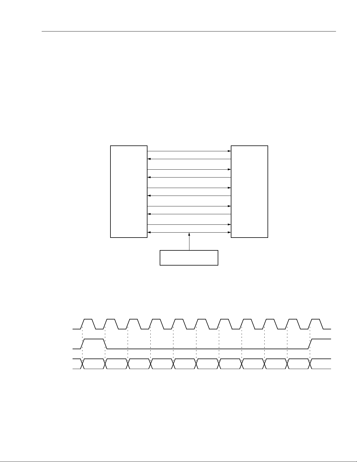
Reduced Media Independent Interface (RMII)
This interface reduces the interconnect circuits
between a MAC and PHY. In switch applications, this
protocol helps to reduce the pin count on the switch
ASIC significantly. A regular 16-pin MII reduces to a
7-pin (8-pin with an optional RXER pin) RMII. The
interconnect circuits are the following:
1. REF_CLK: A 50 MHz clock.
2. TX_EN.
3. TXD[1:0].
4. RXD[1:0].
5. CRS_D V.
6. RXER: Mandator
switch.
for the PHY, but optional for the
MII MAC I/F TO RMII MAC I/F
TXEN
TXD[3:0]
TXER
TXCLK
COL
CRS
RXDV
RXD[3:0]
RXER
RXCLK
MAC RMII PHY
RMII PHY I/F TO MII PHY I/F
TXEN
TXD[1:0]
CRS_DV
RXD[1:0]
RXER
REFCLK
50 MHz
Figure 4. Functional Description
TXEN
TXD[3:0]
TXER
TXCLK
COL
CRS
RXDV
RXD[3:0]
RXER
RXCLK
5-7505(F).r1
Lucent Technologies Inc. 13
LU3X34FTR Preliminary Data Sheet
Quad 3 V 10/100 Ethernet Transceiver TX/FX July 2000
Functional Description
(continued)
Transmit Data Path
The PHY uses the 50 MHz REF_CLK as its reference
so that TXC (at the internal MII) and REF_CLK maintain a phase relationship. This helps to avoid elasticity
buffers on the transmit side. On the rising edge of
REF_CLK, 2-bit data is provided on the RMII TXD[1:0]
when TXEN is high. TXD[1:0] will be 00 to indicate idle
when TXEN is deasserted.
TX 10 Mbits/s Mode
The REF_CLK frequency is ten times the data rate in
this mode; therefore, the value on TXD[1:0] will be valid
such that TXD[1:0] may be sampled every tenth cycle,
regardless of the starting cycle within the group.
TX 100 Mbits/s Mode
There will be valid data on TXD[1:0] for each REF_CLK
period when TXEN is asserted.
Receive Data Path
RXCLK (at the internal MII) is derived from the incoming data and, hence, does not maintain a phase relationship with REF_CLK. Therefore, an elasticity buffer
is required on the receive path. An 8-nibble deep elasticity buffer is required based on the ppm variation of
the clocks. CRS_DV is asserted asynchronously. Preamble is output onto the RMII once the internal signal
RX_DV is asserted (on the rising edge of the
REF_CLK). CRS_DV is deasserted asynchronously
with the fall of RX_DV, but CRS_DV keeps toggling as
long as data is being flushed out of the elasticity buffer.
RX 10 Mbits/s Mode
After the assertion of CRS_DV, the receive data signals, RXD[1:0], will be 00 until the 10Base-T PHY has
recovered the clock and decoded the receive data.
Since REF_CLK is 10 times the data rate in this mode,
the value on RXD[1:0] will be valid such that it can be
sampled every tenth cycle, regardless of the starting
cycle within the group.
RX 100 Mbits/s Mode
After the assertion of CRS_DV, the receive data signals, RXD[1:0] will be 00 until the start-of-stream (SSD)
delimiter has been detected.
Collision Detection
The RMII does not have a collision signal, so all collisions are detected internal to the MAC. This is an AND
function of TXEN and CRS derived from CRS_DV.
CRS_DV cannot be directly ANDed with TXEN,
because CRS_DV may toggle at the end of a frame to
provide separation between CRS and RXDV.
Receiver Error
The RX_ER signal is asserted for one or more
REF_CLK periods to indicate that an error was
detected within the current receive frame.
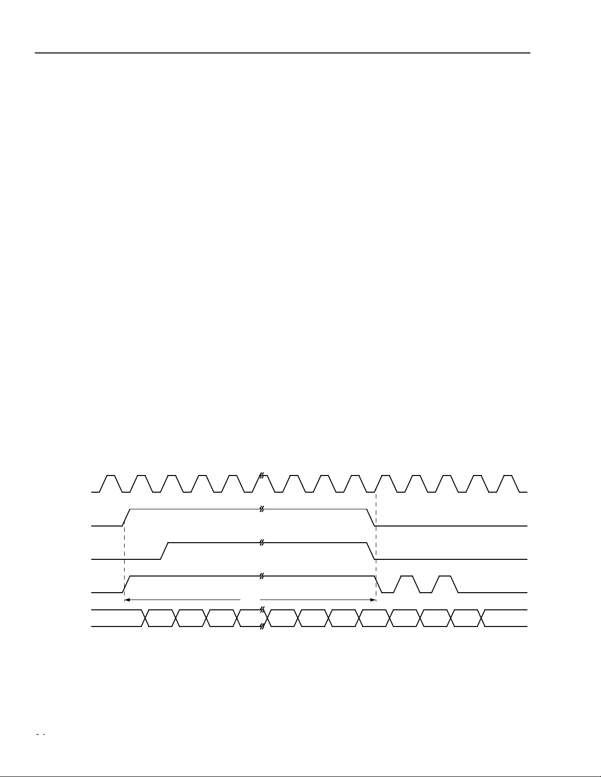
REF_CLK
CRS
RX_DV
CRS_DV
CRS
RMII_RXD[1:0] 00 01 01 00
5-7506(F).r2
Figure 5. RMII Receive Timing from Internal MII Signals
1414 Lucent Technologies Inc.
Preliminary Data Sheet LU3X34FTR
July 2000 Quad 3 V 10/100 Ethernet Transceiver TX/FX
Functional Description
(continued)
Loopback
During normal operation, TXD[1:0] and TX_EN will not be looped back to CRS_DV and RXD[1:0].
Serial Media Independent Interface (SMII)
The SMII allows a further reduction in the number of signals that are required to interface a PHY to a MAC. There
are two global signals, CLK125 and SYNC, and two per-port signals, RXD, TXD. All signals are synchronous to the
125 MHz clock.
MULTI-MAC
SMII_TXD0
SMII_RXD0
SMII_TXD1
SMII_RXD1
SMII_TXD2
SMII_RXD2
SMII_TXD3
SMII_RXD3
LU3X34FTR
PORT 0
PORT 1
PORT 2
PORT 3
REF_CLK
SMII_SYNC
SMII_RXD
SMII_SYNC
REF_CLK
125 MHz
REFERENCE CLOCK
5-7507(F).r4
Figure 6. SMII Connection Diagram
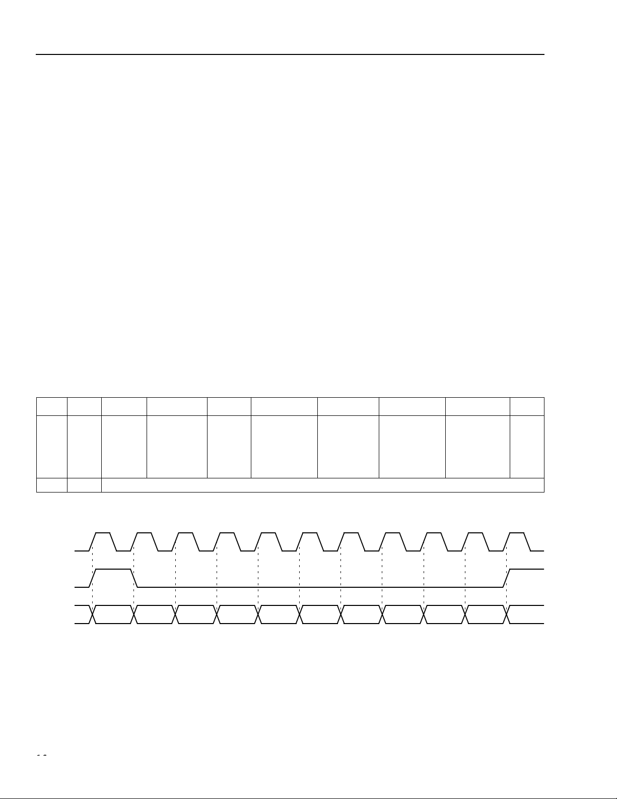
1234567891011
CRS RXDV RXD0 RXD1 RXD2 RXD3 RXD4 RXD5 RXD6 RXD7
5-7507(F).r4
Figure 7. Receive Sequence Diagram
Lucent Technologies Inc. 15
LU3X34FTR Preliminary Data Sheet
Quad 3 V 10/100 Ethernet Transceiver TX/FX July 2000
Functional Description
(continued)
Receive Path
Receive data and control information are signaled in
10-bit segments. These 10-bit boundaries are delimited
by the SYNC signal. The connected MAC should generate these SYNC pulses every ten clocks. In
100 Mbits/s mode, each segment represents a new
byte of data. In 10 Mbits/s mode, each segment is
repeated ten times, so every ten segments represents
a new byte of data.
The receive sequence contains all of the information
found on the standard MII receive path. RXD[7:0] convey packet data whenever the RXDV bit is set. During
an interframe gap, RXDV bit is set to 0 and RXD[7:0]
indicate receiver status. Bit RXD5 indicates the validity
of the upper nibble of the last byte of data of the previous frame. Bit RXD0 indicates an error detected by the
PHY in the previous frame. Both of these bits will be
valid in the segment immediately following a frame, and
will remain valid until the first data segment of the next
frame.
Transmit Data Path
Transmit data and control information are signaled in
10-bit segments similar to the receive path. These
10-bit boundaries are delimited by the SYNC signal.
The connected MAC should generate these SYNC
pulses every ten clocks. In 100 Mbits/s mode, each
new segment represents a new byte of data. In
10 Mbits/s mode, each segment is repeated ten times;
therefore, ev ery ten segments represents a new byte of
data. The PHY can sample one of every ten segments.
The PHY is concerned only with packet data, so there
is no status information passed from the MAC to the
PHY during the interframe gap; this is unlike the
receive side.
Collision Detection
The PHY does not directly indicate that a collision has
occurred. It is left up to the MAC to detect the assertion
of both CRS and TXEN.
Table 10. Receive Data/Status Encoding
CRS RXDV RXD0 RXD1 RXD2 RXD3 RXD4 RXD5 RXD6 RXD7
X0Rcvr
error in
the pre-
10 Mbits/s
vious
frame.
100 Mbits/s
Speed:
0 =
1 =
Duplex:
0 = half
1 = full
Link:
0 = no link
1 = good link
Jabber:
0 = OK
1 = detected
Upper nibble:
0 = invalid
1 = valid
False carrier:
0 = OK
1 = detected
X 1 One Data Byte (two MII nibbles)
1234567891011
SMII_CLK
SYNC
TXD
TXER TXEN TXD0 TXD1 TXD2 TXD3 TXD4 TXD5 TXD6 TXD7
5-7508(F).r1
Figure 8. Transmit Sequence Diagram
1
1616 Lucent Technologies Inc.
 Loading...