

AGERE LU3X31T-T64 Datasheet

Preliminary Data Sheet
July 2000
Overview
The LU3X31T-T64 is a fully integrated
10/100 Mbits/s physical layer device with an integrated transceiver. It is provided in a 64-pin TQFP
package with low-power operation and powerdown
modes. Typical applications for this part are CardBus
and PCMCIA Ethernet products. Operating at 3.3 V,
the LU3X31T-T64 is a powerful device for the f orward
migration of legacy 10 Mbits/s products and noncompliant (does not have autonegotiation) 100 Mbits/s
devices. The LU3X31T-T64 was designed from the
beginning to conform fully with all pertinent specifications, from the
cabling guidelines to
§
IEEE
802.3 Ethernet specifications.
*
ISO
/IEC 11801 and
ANSI
†
EIA
‡
X3.263 TP-PMD to
/TIA 568
Features
■
Single-chip integrated physical layer and transceiver for 10Base-T and/or 100Base-T functions
■
IEEE
802.3 compatible 10Base-T and 100Base-T
physical layer interface and
compatible transceiver
■
Built-in analog 10 Mbits/s receive filter, eliminating
the need for external filters
ANSI
X3.263 TP-PMD
LU3X31T-T64 Single-Port 3 V
10/100 Ethernet Transceiver TX
■
100 Mbits/s PLL, combined with the digital adaptive equalizer, robustly handles variations in risefall time, excessive attenuation due to channel
loss, duty-cycle distortion, crosstalk, and baseline
wander
■
Transmit rise-fall time can be manipulated to provide lower emissions, amplitude fully compatible
for proper interoperability
■
Programmable scrambler seed for better FCC
compliancy
■
IEEE
802.3u Clause 28 compliant autonegotiation
for full 10 Mbits/s and 100 Mbits/s control
■
Fully configurable via pins and management
accesses
■
Extended management support with interrupt
capabilities
■
PHY MIB support
■
Symbol mode option
■
Low-power operation: <150 mA max
■
Low autonegotiation power: <30 mA
■
Very low powerdown mode: <5 mA
■
64-pin TQFP package (10 mm x 10 mm x 1.4 mm)
■
Built-in 10 Mbits/s transmit filter
■
10 Mbits/s PLL exceeding tolerances for both preamble and data jitter
*
ISO
is a registered trademark of The International Organization
for Standardization.
†
EIA
is a registered trademark of The Electronic Industries Asso-
ciation.
ANSI
is a registered trademark of The American National Stan-
‡
dards Institute, Inc.
§
IEEE
is a registered trademark of The Institute of Electrical and
Electronics Engineers, Inc.

LU3X31T-T64 Single-Port 3 V Preliminary Data Sheet
10/100 Ethernet Transceiver TX July 2000
Table of Contents
Contents Page
Overview................................................................................................................................................................... 1
Features ................................................................................................................................................................... 1
Pin Descriptions........................................................................................................................................................ 6
Functional Description............................................................................................................................................ 10
Media Independent Interface (MII)...................................................................................................................... 10
100Base-X Module.............................................................................................................................................. 11
100Base-X Receiver ........................................................................................................................................... 14
100Base-X Link Monitor...................................................................................................................................... 15
100Base-TX Transceiver..................................................................................................................................... 16
10Base-T Module................................................................................................................................................ 16
Clock Synthesizer................................................................................................................................................ 18
Autonegotiation ................................................................................................................................................... 18
Reset Operation.................................................................................................................................................. 19
100Base-X PCS Configuration............................................................................................................................ 20
MII Registers ............................................................. ...... ....... ...... ....................................... ...... ....... ...... ....... ...... ... 21
dc and ac Specifications......................................................................................................................................... 31
Absolute Maximum Ratings................................................................................................................................. 31
Clock Timing........................................................................................................................................................... 32
Outline Diagram...................................................................................................................................................... 43
64-Pin TQFP ............. ...... ...... ....... ............................................. ....... ...... ...... ................................ . ...... ....... ......... 43
Ordering Information............................................................................................................................................... 44
Tables Page
Table 1. Twisted-Pair Magnetic Interface ................................................................................................................. 5
Table 2. Twisted-Pair Transceiver Control................................................................................................................ 6
Table 3. MII Interface............................................................................................................................................... 6
Table 4. PHY Address Configuration ....................................................................................................................... 7
Table 5. 100Base-X PCS Configuration................................................................................................................... 7
Table 6. Autonegotiation Configuration.................................................................................................................... 7
Table 7. LED and Status Outputs ............................................................................................................................ 8
Table 8. Clock and Chip Reset ................................................................................................................................ 9
Table 9. Power and Ground ..................................................................................................................................... 9
Table 10. Symbol Code Scrambler ........................................................................................................................ 13
Table 11. Autonegotiation ...................................................................................................................................... 20
Table 12. MII Management Registers.................................................................................................................... 20
Table 13. Control Register (Register 0h) ............................................................................................................... 21
Table 14. Status Register (Register 1h)................................................................................................................. 23
Table 15. PHY Identifier (Register 2h) ................................................................................................................... 25
Table 16. PHY Identifier (Register 3h) ................................................................................................................... 25
Table 17. Autonegotiation Advertisement (Register 4h) ........................................................................................ 25
Table 18. Autonegotiation Link Partner Ability (Register 5h) ................................................................................. 25
Table 19. Autonegotiation Expansion Register (Register 6h) ................................................................................ 26
Table 20. Receive Error Counter (Register 15h).................................................................................................... 26
Table 21. PHY Control/Status Register (Register 17h).......................................................................................... 27
Table 22. Config 100 Register (Register 18h)........................................................................................................ 28
Table 23. PHY Address Register (Register 19h) ................................................................................................... 29
Table 24. Config 10 Register (Register 1Ah) ......................................................................................................... 29
Table 25. Status 100 Register (Register 1Bh) ....................................................................................................... 30
Table 26. Status 10 Register (Register 1Ch)......................................................................................................... 30
2 Lucent Technologies Inc.

Preliminary Data Sheet LU3X31T-T64 Single-Port 3 V
July 2000 10/100 Ethernet Transceiver TX
Table of Contents
Tables
Table 27. Interrupt Mask Register (Register 1Dh).................................................................................................. 30
Table 28. Interrupt Status Register (Register 1Eh) ................................................................................................31
Table 29. Absolute Maximum Ratings.................................................................................................................... 31
Table 30. Operating Conditions.............................................................................................................................. 31
Table 31. dc Characteristics................................................................................................................................... 32
Table 32. System Clock (Xin)................................................................................................................................. 32
Table 33. Transmit Clock (Input and Output).......................................................................................................... 33
Table 34. Management Clock................................................................................................................................. 34
Table 35. MII Receive Timing................................................................................................................................. 35
Table 36. MII Transmit Timing ................................................................................................................................36
Table 37. Transmit Timing ......................................................................................................................................37
Table 38. Receive Timing....................................................................................................................................... 38
Table 39. Reset and Configuration Timing.............................................................................................................39
Table 40. PMD Characteristics............................................................................................................................... 40
(continued)
(continued)
Page
Figures Page
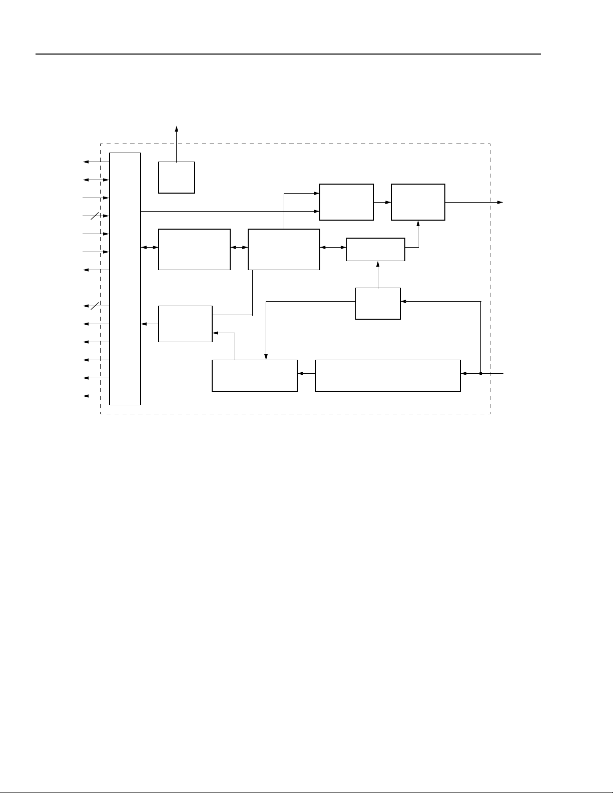
Figure 1. LU3X31T-T64 Block Diagram ................................................................................................................... 4
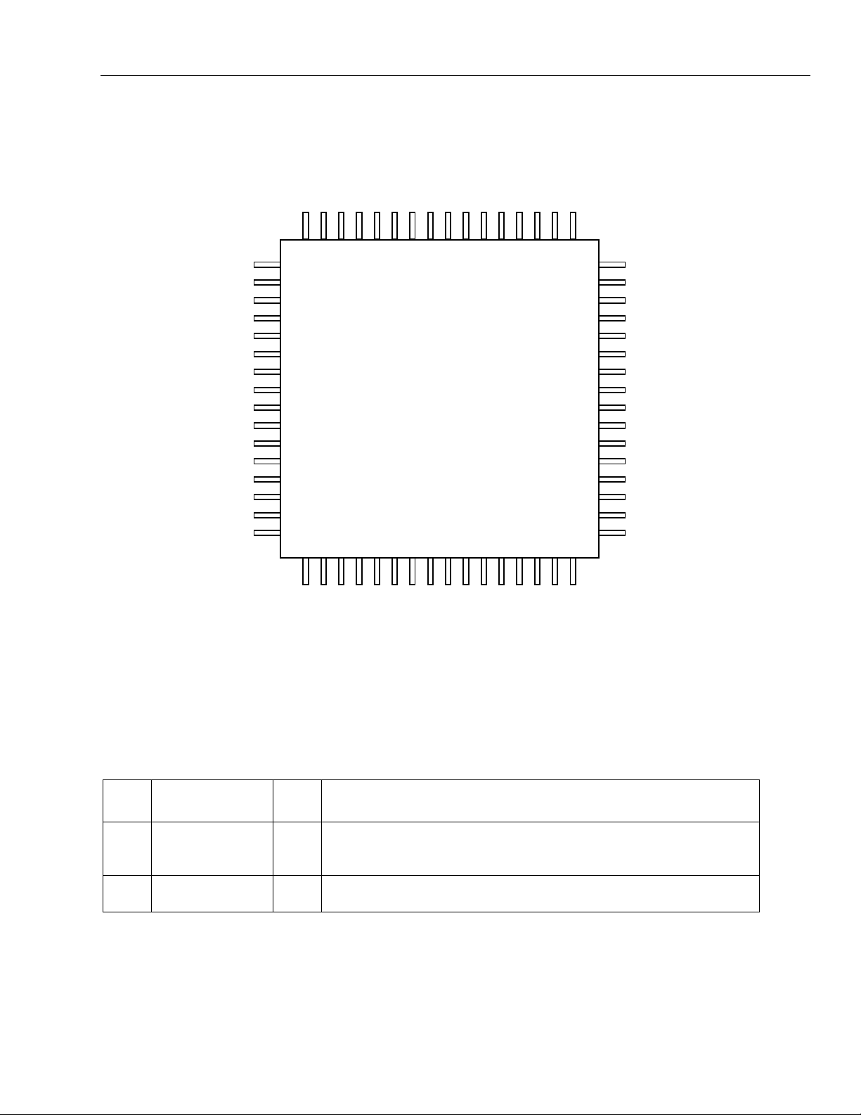
Figure 2. Pin Diagram..............................................................................................................................................5
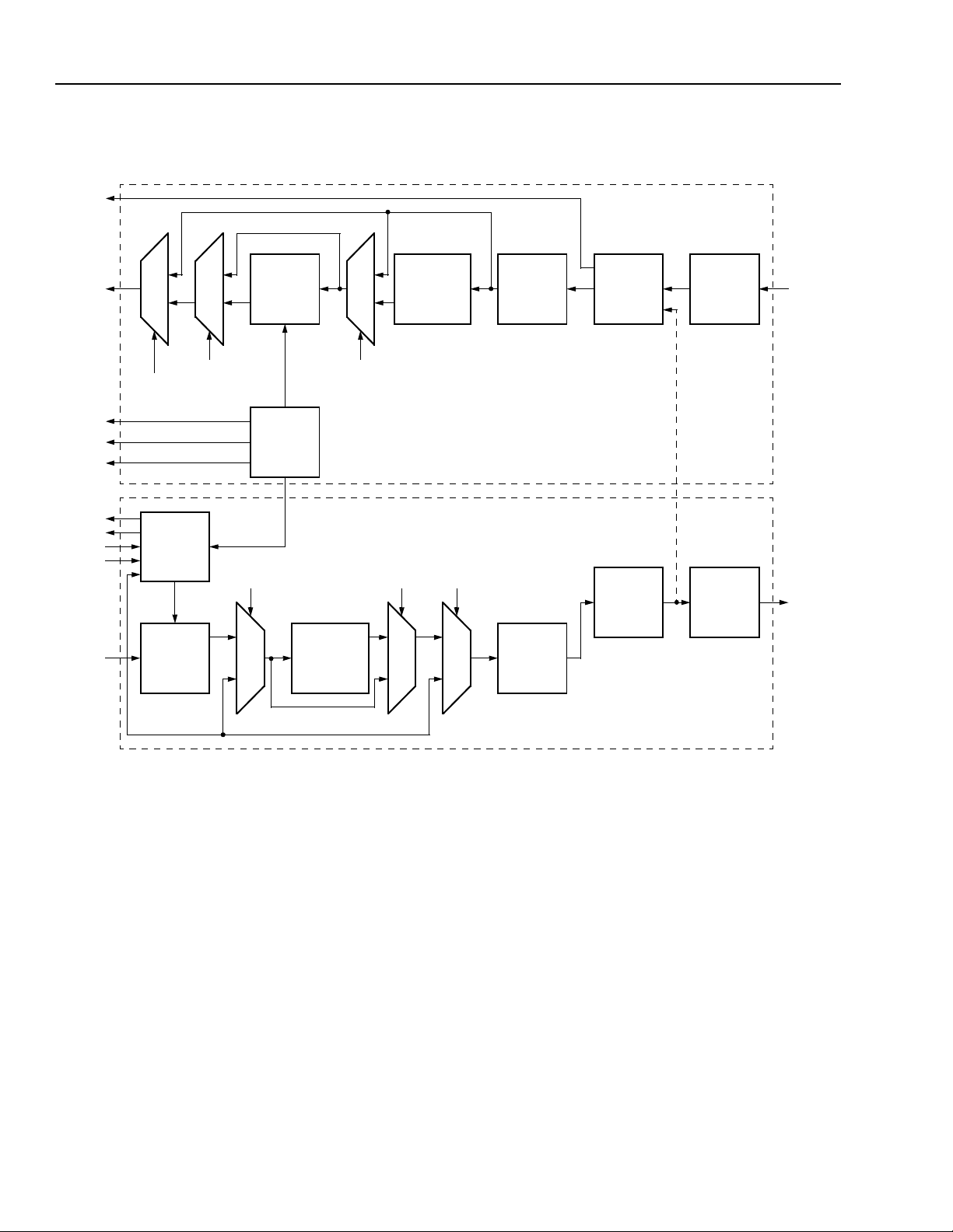
Figure 3. 100Base-X Data Path........... ....... ...... ....... ...... ....... ...... ...... ......................................... ..... ...... ....... ...... .... 12
Figure 4. 10Base-T Module Data Path .................................................................................................................. 16
Figure 5. Hardware Reset Configurations..............................................................................................................19
Figure 6. System Timing........................................................................................................................................ 32
Figure 7. Transmit Timing (Input and Output) ........................................................................................................33
Figure 8. Management Timing............................................................................................................................... 34
Figure 9. MII Receive Timing.................................................................................................................................35
Figure 10. MII Transmit Timing .............................................................................................................................. 36
Figure 11. Transmit Timing .................................................................................................................................... 37
Figure 12. Receive Timing.....................................................................................................................................38
Figure 13. Reset and Configuration Timing........................................................................................................... 39
Figure 14. PMD Timing..........................................................................................................................................40
Figure 15. Connection Diagrams (Frequency References)....................................................................................41
Figure 16. Connection Diagrams (10/100BTX Operation).....................................................................................42
Lucent Technologies Inc. 3
LU3X31T-T64 Single-Port 3 V Preliminary Data Sheet
10/100 Ethernet Transceiver TX July 2000
Features
MDIOINTZ
MDIO
MDC
TXD
TXEN
TXER
TXCLK
RXD
RXDV
RXER
RXCLK
COL
(continued)
MII
INTERFACE LOGIC
S
LED
S
LED
MANAGEMENT
INTERFACE
10/100-RX
PCS
REGISTER/
CONFIG/
CONTROL
CLOCK SYNTHESIS
AND RECOVERY
10/100-TX
PCS
AUTONEG
RX10
SQUELCH
ADAPTIVE EQUALIZER
BASELINE WANDER CORRECTION
10/100-TX
DRIVERS
TPTX
TPRX
±
±
CRS
5-6779(F).ar.2
Figure 1. LU3X31T-T64 Block Diagram
4 Lucent Technologies Inc.
Preliminary Data Sheet LU3X31T-T64 Single-Port 3 V
July 2000 10/100 Ethernet Transceiver TX
Features
MDIOINTZ/PHY[2]
(continued)
RESV
100FDEN
GND9
AUTONEN
TPTXTR
EQGND1
DD
EQV
RESV
RSTZ
PHY[0]
100HDEN
DD
V
GND1
DD
V
TPRX+
RXGND1
1
DD
TPTX+
1
DD
TXGND1
TXV
REF100
REF10
49
32TXD0
48
47
46
45
44
43
42
41
40
39
38
37
36
35
34
33
XOUT
XIN
DD
XTLV
MDC
LNKLED/BPALIGN
LEDFD/10HDEN
LEDCOL/BP4B5B
LEDTX/ACTLED/BPSCR
LEDRX
COL/PHY[4]
DD
6
V
DD
4
V
GND4
MDIO
CRS/PHY[3]
TXCLK
2
DD
DD
TPTX–
TXV
CSGND
CSV
CSVDDRXV
2
DD
TPRX–
RXGND2
RXV
646362616059585756555453525150
1
2
3
4
5
6
1
5
1
7
8
9
10
11
12PHY[1]
13
14
15
16
171819202122232425262728293031
RXER
RXDV
LEDSP/10FDEN
Table 1. Twisted-Pair Magnetic Interface
Pin
No.
53
54
Pin Name I/O Pin Description
TPTX+
TPTX–
Twisted-Pair Transmit Driver Pair.
O
100Base-T MLT-3 signals on Category 5 UTP cable or 10Base-T
Manchester signals on Category 3 UTP cable.
61
62
TPRX+
TPRX–
Twisted-Pair Receive Pair.
I
10Base-T Manchester data.
8
DD
V
RXD0
RXD1
RXD2
RXD3
RXCLK
GND8
Figure 2. Pin Diagram
TXD1
TXD2
TXD3
TXER
TXEN
These pins are used to transmit
These pins receive 100Base-T MLT 3 or
5-6780(F).br.5
Lucent Technologies Inc. 5

LU3X31T-T64 Single-Port 3 V Preliminary Data Sheet
10/100 Ethernet Transceiver TX July 2000
Pin Descriptions
Table 2. Twisted-Pair Transceiver Control
Pin
No.
Pin Name I/O Pin Description
50 REF100 I
49 REF10 I
5TPTXTRI
Table 3. MII Interface
Pin
No.
Pin Name I/O Pin Description
18 RXDV O
19 RXER O
20 RXD3 O
21 RXD2 O
22 RXD1 O
23 RXD0 O
24 RX CLK O
27 TXEN I
28 TXER I
29 TXD3 I
30 TXD2 I
31 TXD1 I
32 TXD0 I
33 TXCLK O
34 CRS/
39 COL/
PHY[3]
PHY[4]
I/O
I/O
35 MDIO I/O
45 MDC I
16 MDIOINTZ/
PHY[2]
I/O
Reference Resistor for 100 Mbits/s Twisted-Pair Driver.
Connect
this pin to ground through a 301 Ω resistor.
Reference Resistor for 10 Mbits/s Twisted-Pair Driver.
Connect
this pin to ground through a 4.64 kΩ resistor.
Twisted-Pair Transmitter 3-State.
A high on this pin will 3-state the
twisted-pair outputs. Tie to ground in normal operation.
Receive Data Valid.
Receive Error.
Signals the presence of data on RXD[3:0].
Indicates a received coding error has occurred.
Receive Data[3].
Receive Data[2].
Receive Data[1].
Receive Data[0].
Receive Clock.
Transmit Enable.
Transmit Error.
Signals the presence of data on TXD[3:0].
Indicates a transmit coding error has occurred.
Transmit Data[3].
Transmit Data[2].
Transmit Data[1].
Transmit Data[0].
Transmit Clock.
Carrier Sense/PHY Address[3].
This output pin indicates the carrier
sense condition. See Table 4 for PHY[3] description.
Collision/False Carrier Sense.
This output pin indicates collision
condition in normal MII operation and is squelch jabber in 10 Mbits/s
mode. See Table 4 for PHY[4] description.
Management Data I/O.
Management Data Clock.
MDIO Interrupt (Active-Low).
Serial access to device config registers.
Clock for R/W of device config registers.
The MDIO int errupt pin out puts a l ogi c
0 pulse of 40 ns, synchronous to XIN, whenever an unmasked interrupt condition is detected. Refer to management registers 1Dh and
1Eh for interrupt conditions. See Table 4 for PHY[2] description.
Note: Smaller font indicates that the pin has multiple functions.
6 Lucent Technologies Inc.

Preliminary Data Sheet LU3X31T-T64 Single-Port 3 V
July 2000 10/100 Ethernet Transceiver TX
Pin Descriptions
(continued)
Table 4. PHY Address Configuration
Pin
No.
10
12
16
34
39
Note: Smaller font indicates that the pin has multiple functions.
Pin Name I/O Pin Description
PHY[0]
PHY[1]
PHY[2]/
PHY[3]/
PHY[4]/
MDIOINTZ
CRS
COL
PHY Address[4:0].
I
initialize the PHY address used for MII management register interface. PHY
I
address 00h forces the PHY into MII isolate mode. PHY address pins[4:2]
I/O
have an internal 40 kΩ pull-down resistor. See Table 3 for MDIOINTZ, CRS,
I/O
and COL description.
I/O
Table 5. 100Base-X PCS Configuration
Pin
No.
41 BPSCR/
Pin Name I/O Pin Description
Bypass Scrambler Mode.
I/O
will bypass the scramble/descramble operations in 100Base-X data path.
ACTLED
LEDTX
/
This pin has an internal 40 kΩ pull-down resistor. See Table 7 for LEDTX/
ACTLED de scri ption.
42 BP4B5B/
LEDCOL
Bypass 4B/5B Mode.
I/O
bypass the 4B/5B encoder of the PHY. This pin has an internal 40 kΩ pulldown resistor. See Table 7 for LEDCOL description.
44 BPALIGN/
LNKLED
Bypass Alignment Mode.
I/O
will bypass the alignment feature of the PHY. This bypass mode provides a
symbol interface. This pin has an internal 40 kΩ pull-down. See Table 7 for
LNKLED description.
Note: Smaller font indicates that the pin has multiple functions.
These 5 pins are detected during powerup or reset to
A high value on this pin during powerup or reset
A high value on this pin during powerup or reset will
A high value on this pin during powerup or reset
Table 6. Autonegotiation Configuration
Pin
No.
Pin Name I/O Pin Description
4AUTONENI
(Refer to Table 11.)
Autonegotiation Enable.
will enable autonegotiation; a low value will disable it.
2 100FDEN I
100 Full-Duplex Enable.
or reset to determine whether 100 Mbits/s full-duplex mode is available.
When autonegotiation is enabled, this input sets the ability register bit in
advertisement register 4. When autonegotiation is not enabled, this input
will select the mode of operation.
11 100HDEN I
100 Half-Duplex Enable.
or reset to determine whether 100 Mbits/s half-duplex mode is available.
When autonegotiation is enabled, this input sets the ability register bit in
advertisement register 4. When autonegotiation is not enabled, this input
will select the mode of operation.
17 10FDEN/
LEDSP
10 Full-Duple x Enable.
I/O
powerup or reset to determine whether 10 Mbits/s full-duplex mode is available. When autonegotiation is enabled, this input sets the ability register bit
in advertisement register 4. When autonegotiation is not enabled, this input
will select the mode of operation. This pin has an internal 40 kΩ pull-up
resistor. See Table 7 for LEDSP description.
Note: Smaller font indicates that the pin has multiple functions.
A high value on this pin during powerup or reset
The logic level of this pin is detected at powerup
The logic level of this pin is detected at powerup
The logic level of this pin is detected at
Lucent Technologies Inc. 7

LU3X31T-T64 Single-Port 3 V Preliminary Data Sheet
10/100 Ethernet Transceiver TX July 2000
Pin Descriptions
Table 6. Autonegotiation Configuration
Pin
No.
43 10HDEN/
Pin Name I/O Pin Description
(continued)
LEDFD
(Refer to Table 11.) (continued)
10 Half-Duplex Enable.
I/O
reset to determine whether 10 Mbits/s half-duplex mode is available. When
autonegotiation is enabled, this input sets the ability register bit in advertisement register 4. When autonegotiation is not enabled, this input will select
the mode of operation. This pin has an internal 40 kΩ pull-up resistor. See
Table 7 for L EDFD des cription.
Note: Smaller font indicates that the pin has multiple functions.
Table 7. LED and Status Outputs
Pin
No.
40 LEDRX I/O
Pin Name I/O Pin Description
Receive LED.
receiving data from the UTP cable. This pin has an internal 40 kΩ pull-down
resistor. The LED should be connected as logic 0 configuration as shown in
Figure 5, without the 10 kΩ re si st or.
41 LEDTX/ACTLED/
BPSCR
Transmit LED or Activity LED.
I/O
will drive a 10 mA LED if the LU3X31T-T64 is transmitting data. If the control
bit is set, then the LED will be driven whenever receive or transmit activity is
present. This pin has an internal 40 kΩ pull-down. The LED should be connected as LOGIC 0 configuration in Figure 5 without the 10 kΩ resistor. See
Table 5 for BPSCR description.
44 LNKLED/
BPALIGN
I/O
Link LED.
This output will drive a 10 mA LED for as long as a valid link
exists across the cable. Place a 10 kΩ resistor across the LED pins if setting
to nondefault mode, i.e., bypass align mode as shown in Figure 5. See Table
5 for BPALIGN description.
42 LEDCOL/
BP4B5B
Collision LED.
I/O
T64 senses a collision has occurred. Place a 10 kΩ resistor across the LED
pins if setting to nondefault mode, i.e., bypass 4B/5B mode as shown in Figure 5. See Table 5 for BP4B5B description.
43 LEDFD/
10HDEN
Full-Duplex Status.
I/O
T64 is in full-duplex mode. Place a 10 kΩ resistor across the LED pins if setting to nondefault mode, i.e., 10HD disable mode as shown in Figure 5. See
Table 6 for 10HDEN description.
17 LEDSP/
10FDEN
Speed Status.
I/O
is in 100 Mbits/s mode. Place a 10 kΩ resistor across the LED pins if setting
to nondefault mode, i.e., 10FD disable mode as shown in Figure 5. See
Table 6 for 10FDEN description.
Note: Smaller font indicates that the pin has multiple functions.
The logic level of this pin is detected at powerup or
This output will drive a 10 mA LED if the LU3X31T-T64 is
When bit 7 of register 17h is 0, this output
This output will drive a 10 mA LED whenever the LU3X31T-
This output will drive a 10 mA LED when the LU3X31T-
This output will drive a 10 mA LED when the LU3X31T-T64
8 Lucent Technologies Inc.

Preliminary Data Sheet LU3X31T-T64 Single-Port 3 V
July 2000 10/100 Ethernet Transceiver TX
Pin Descriptions
(continued)
Table 8. Clock and Chip Reset
Pin
No.
Pin Name I/O Pin Description
47 XIN I
48 XOUT O
9RSTZI
1
RESV —
8
Table 9. Power and Ground
Plane
Name Pin Number Na me Pin Number
RXV
TXV
CSV
V
V
V
V
DD
DD
DD
DD
DD
DD
DD
DD
DD
DD
DD
1
4
5
6
8
RX Analog RXV
TX Analog TXV
CS CSV
Digital V
—
DD
EQV
Clock XTLV
Crystal Oscillator Input or Clock Input.
See Figure 15 for a con-
nection diagram.
Crystal Oscillator Feedback Output.
If a single-ended external
clock is connected to XIN pin, then XOUT should be grounded for
minimum power consumption. See Figure 15 for a connection diagram.
Reset (Active-Low).
This input must be held low for a minimum of
1 ms to reset the LU3X31T-T64.
Reserved.
These pins are unused inputs and should be tied to
ground.
V
CC Pin Associated Ground Pin
1
2
1
2
1
DD
59
64
51
55
57
58
15
37
13
38
25
—
7
RXGND1
RXGND2
TXGND1
—
CSGND
—
GND1
GND4
—
—
GND8
GND9
EQGND1
60
63
52
—
56
—
14
36
—
—
26
3
6
46 — —
Lucent Technologies Inc. 9

LU3X31T-T64 Single-Port 3 V Preliminary Data Sheet
10/100 Ethernet Transceiver TX July 2000
Functional Description
The LU3X31T-T64 integrates a 100Base-X physical
sublayer (PHY), a 100Base-TX physical medium
dependent (PMD) transceiver, and a complete 10BaseT module into a single chip for both 10 Mbits/s and
100 Mbits/s Ethernet operation. This device provides
an
IEEE
802.3u compliant media independent interface
(MII) to communicate between the physical signaling
and the medium access control (MAC) layers for both
100Base-X and 10Base-T operations. The device is
capable of operating in either full-duplex mode or halfduplex mode in either 10 Mbits/s or 100 Mbits/s operation. Operational modes can be selected by hardware
configuration pins, selected by software settings of
management registers, or determined by the on-chip
autonegotiation logic.
The 10Base-T section of the device consists of the
10 Mbits/s transceiver module with filters and a
Manchester ENDEC module.
The 100Base-X section of the device implements the
following functional blocks:
■
100Base-X physical coding sublayer (PCS)
■
100Base-X physical medium attachment (PMA)
■
Twisted-pair transceiver
The 100Base-X and 10Base-T sections share the following functional blocks:
■
Clock synthesizer module (CSM)
■
MII registers
■
IEEE
802.3u autonegotiation
Each of these functional blocks is described below.
Media Independent Interface (MII)
size data path, TXEN signals the presence of data on
TXD, TXER indicates that a transmit coding error has
occurred, and TXCLK is the transmit clock that synchronizes all the transmit signals. TXCLK is supplied by
the on-chip clock synthesizer.
Receive Data Int erfac e.
The MII rec eiv e data interf ac e
comprises seven signals: RXD[3:0] are the nibble size
data path, RXDV signals the presence of data on RXD,
RXER indicates a received coding error, and RXCLK is
the receive clock. Depending upon the operation mode,
RXCLK is generated by the clock recovery module of
either the 100Base-X or 10Base-T receiver.
Status Interface.
Two status signals, COL and CRS,
are generated in the LU3X31T-T64 to indicate collision
status and carrier sense status to the MAC. COL is
asserted asynchronously whenever LU3X31T-T64 is
transmitting and receiving at the same time in a halfduplex operation mode. In the full-duplex mode, COL is
inactive. CRS is asserted asynchronously whenever
there is activity on either the transmitter or the receiver.
In full-duplex mode, CRS is asserted only when there is
activity on the receiver.
Operation Modes
The LU3X31T-T64 supports three operation modes
and an isolate mode as described below.
100 Mbits/s Mode.
For 100 Mbits/s operation, the MII
operates in nibble mode with a clock rate of 25 MHz. In
normal operation, the MII data at RXD[3:0] and
TXD[3:0] are 4 bits wide. In bypass mode (either
BYP_4B5B or BYP_ALIGN option selected), the MII
data takes the form of 5-bit code-groups. The least significant 4 bits appear on TXD[3:0] and RXD[3:0] as
usual, and the most significant bits (TXD[4] and
RXD[4]) appear on the TXER and RXER pins, respectively.
The LU3X31T-T64 implements an
IEEE
22 compliant MII as described below.
802.3u Clause
10 Mbits/s Mode.
and RXCLK operate at 2.5 MHz. The data paths are
For 10 Mbits/s operation, the TXCLK
always 4 bits wide using TXD[3:0] and RXD[3:0] signal
Interface Signals
Transmit Data Interface.
The MII transmit data inter-
lines.
face comprises seven signals: TXD[3:0] are the nibble
10 Lucent Technologies Inc.

Preliminary Data Sheet LU3X31T-T64 Single-Port 3 V
July 2000 10/100 Ethernet Transceiver TX
Functional Description
(continued)
provided for the MDIO to avoid contention. Following
the turnaround time, a 16-bit data stream is read from
MII Isolate Mode.
The LU3X31T-T64 implements an
MII isolate mode that is controlled by bit 10 of the control register (register 0h). The LU3X31T-T64 will set this
bit to one if the PHY address is set to 00000 upon powerup/hardware reset. Otherwise, the LU3X31T-T64 will
initialize this bit to 0. Setting this bit to a 1 will put the
LU3X31T-T64 into isolate mode.
The isolate mode can also be activated by setting the
PHY address (bits 15 through 11 of register 19h) to 0
through the serial management interface, although the
content of the isolate register is not affected by the
modification of PHY address.
or written into the MII management registers of the
LU3X31T-T64.
The LU3X31T-T64 supports a preamble suppression
mode as indicated by a 1 in bit 6 of the basic mode status register (BMSR, address 01h). If the station management entity (i.e., MAC or other management
controller) determines that all PHYs in the system support preamble suppression by returning a 1 in this bit,
then the station management entity need not generate
preamble for each management transaction. The
LU3X31T-T64 requires a single initialization sequence
of 32 bits of preamble following powerup/hardware
reset. This requirement is generally met by the manda-
The LU3X31T-T64 does not respond to packet data
present at TXD[3:0], TXEN, and TXER inputs and presents a high impedance on the TXCLK, RXCLK, RXD V,
RXER, RXD[3:0], COL, and CRS outputs. The
LU3X31T-T64 will continue to respond to all management transactions.
Serial Management Interface
tory pull-up resistor on MDIO or the management
access made to determine whether preamble suppression is supported. While the LU3X31T-T64 will respond
to management accesses without preamble, a minimum of one idle bit between management transactions
is required as specified in
IEEE
802.3u.
The PHY device address for LU3X31T-T64 is stored in
the PHY address register (register address 19h). It is
The serial management interface (SMI) is the part of
the MII that is used to control and monitor status of the
LU3X31T-T64. This mechanism corresponds to the MII
initialized by the five I/O pins designated as PHY[4:0]
during powerup or hardware reset and can be changed
afterward by writing into register address 19h.
specification for 100Base-X (Clause 22) and supports
registers 0 through 6. Additional vendor-specific registers are implemented within the range of 16 to 31. All
the registers are described in MII Registers on page 21
of this data sheet.
MDIO Interrupt.
rupt capability that can be used to notify the management station of certain events. It generates an activehigh interrupt signal on the MDIOINTZ output pin
The LU3X31T-T64 implements inter-
whenever one of the interrupt status registers (register
Management Register Access.
The SMI consists of
two pins, management data clock (MDC) and management data input/output (MDIO). The LU3X31T-T64 is
designed to support an MDC frequency ranging up to
the
IEEE
specification of 2.5 MHz. The MDIO line is bi-
directional and may be shared by up to 32 devices.
The MDIO pin requires a 1.5 kΩ pull-up resistor which,
during IDLE and turnaround periods, will pull MDIO to
a logic 1 state. Each MII management data frame is
64 bits long. The first 32 bits are preamble consisting of
32 contiguous logic 1 bits on MDIO and 32 correspond-
address 1Eh) becomes set while its corresponding
interrupt mask register (register address 1Dh) is
unmasked. Reading the interrupt status register (register 1Eh) shows the source of the interrupt and clears
the interrupt output signal.
In addition to the MDIOINTZ pin, the LU3X31T-T64 can
also support the interrupt scheme used by the
derLAN
*
MAC. This option can be enabled by setting
TI Thun-
bit 11 of register 17h. Whenever this bit is set, the interrupt is signaled through both the MDIOINTZ pin and
embedded in the MDIO signal.
ing cycles on MDC. Following preamble is the start-offrame field indicated by a <01> pattern. The next field
signals the operation code (OP): <10> indicates READ
from MII management register operation, and <01>
indicates WRITE to MII management register operation. The next two fields are PHY device address and
MII management register address. Both of them are
5 bits wide, and the most significant bit is transferred
first.
100Base-X Module
The LU3X31T-T64 implements a 100Base-X compliant
PCS and PMA and 100Base-TX compliant TP-PMD as
illustrated in Figure 3. Bypass options for each of the
major functional blocks within the 100Base-X PCS provides flexibility for various applications. 100 Mbits/s
PHY loopback is included for diagnostic purposes.
During READ operation, a 2-bit turnaround (TA) time
spacing between register address field and data field is
*TI is a registered trademark and
Texas Instruments, Inc.
ThunderLAN
is a trademark of
Lucent Technologies Inc. 11
LU3X31T-T64 Single-Port 3 V Preliminary Data Sheet
10/100 Ethernet Transceiver TX July 2000
Functional Description
RXCLK
RXD[3:0]
CRS
RXDV
RXER
COL
TXCLK
TXEN
TXER
BYP-ALIGN
TRANSMIT
STATE
MACHINE
DECODE
RECEIVE
STATE
MACHINE
BYP-4B5B BYP-SCR BYP-ALIGN
(continued)
5B/4B
SCRAMBLER
BYP-SCRBYP-4B5B
100BASE-X RECEIVER
100BASE-X TRANSMITTER
DE-
SERIAL
TO
PARALLEL
CLOCK
RECOVERY
100 Mbit PHY
LOOPBACK PATH
MLT-3
STATE
MACHINE
EQUALIZER
10/100
TRANSMIT
DRIVER
TPRX
TPTX
±
±
TXD[3:0]
4B/5B
ENCODE
SCRAMBLER
Figure 3. 100Base-X Data Path
100Base-X Transmitter
The 100Base-X transmitter consists of functional
blocks which convert synchronous 4-bit nibble data, as
provided by the MII, to a 125 Mbits/s serial data
stream. The LU3X31T-T64 implements the 100Base-X
transmit state machine as specified in the
IEEE
802.3u
Standard, Clause 24 and comprises the following functional blocks in its data path:
■
Symbol encoder
■
Scrambler block
■
Parallel/serial converter and NRZ/NRZI encoder
block
Symbol Encoder.
The symbol encoder converts 4-bit
(4B) nibble data generated by the MAC into 5-bit (5B)
PARALLEL
TO
SERIAL
5-6781(F).ar.2
symbols for transmission. This conversion is required
to allow control symbols to be combined with DATA
symbols. Refer to the table below for 4B to 5B symbol
mapping.
Following onset of the TXEN signal, the 4B/5B symbol
encoder replaces the first two nibbles of the preamble
from the MAC frame with a /J/K code-group pair (11000
10001) start-of-stream delimiter (SSD). The symbol
encoder then replaces subsequent 4B codes with corresponding 5B symbols. Following negation of the
TXEN signal, the encoder substitutes the first two IDLE
symbols with a /T/R code-group pair (01101 00111)
end-of-stream delimiter (ESD) and then continuously
injects IDLE symbols into the transmit data stream until
the next transmit packet is detected.
12 Lucent Technologies Inc.

Preliminary Data Sheet LU3X31T-T64 Single-Port 3 V
July 2000 10/100 Ethernet Transceiver TX
Functional Description
Assertion of the TXER input while the TXEN input is
also asserted will cause the LU3X31T-T64 to substitute
HALT code-groups for the 5B code derived from data
present at TXD[3:0]. However, the SSD (/J/K) and ESD
(/T/R) will not be substituted with HALT code-groups.
Hence, the assertion of TXER while TXEN is asserted
Table 10. Symbol Code Scrambler
Symbol
Name
0 11110 0000 DATA 0
1 01001 0001 DATA 1
2 10100 0010 DATA 2
3 10101 0011 DATA 3
4 01010 0100 DATA 4
5 01011 0101 DATA 5
6 01110 0110 DATA 6
7 01111 0111 DATA 7
8 10010 1000 DATA 8
9 10011 1001 DATA 9
A 10110 1010 DATA A
B 10111 1011 DATA B
C 11010 1100 DATA C
D 11011 1101 DATA D
E 11100 1110 DATA E
F 11101 1111 DATA F
I 11111 undefined IDLE: interstream fill code
J 11000 0101 First start-of-stream delimiter
K 10001 0101 Second start-of-stream delimiter
T 01101 undefined First end-of-stream delimiter
R 001 11 undefined Second end-of-stream deli mi ter
H 00100 undefined HALT: transfer error
V 00000 undefined Inval id cod e
V 00001 undefined Inval id cod e
V 00010 undefined Inval id cod e
V 00011 undefined Inval id cod e
V 00101 undefined Inval id cod e
V 00110 undefined Inval id cod e
V 01000 undefined Inval id cod e
V 01100 undefined Inval id cod e
V 10000 undefined Inval id cod e
V 11001 undefined Inval id cod e
5B Code
[4:0]
(continued)
4B Code
[3:0]
will result in a frame properly encapsulated with the /J/
K and /T/R delimiters which contains HALT codegroups in place of the DATA code-groups.
The 100 Mbits/s symbol decoder translates all invalid
code groups into 0Eh by default. In case the ACCEPT
HALT register is set (bit 5 of register 18h), the HALT
code-group (00100) is translated into 05h instead.
Interpretation
Lucent Technologies Inc. 13

LU3X31T-T64 Single-Port 3 V Preliminary Data Sheet
10/100 Ethernet Transceiver TX July 2000
Functional Description
Scrambler.
For 100Base-TX applications, the scram-
(continued)
bler is required to control the radiated emissions at the
media connector and on the twisted-pair cable.
The LU3X31T-T64 implements a data scrambler as
defined by the TP-PMD stream cipher function. The
scrambler uses an 11-bit ciphering linear feedback shift
register (LFSR) with the following recursive linear function:
X[n] = X[n – 11] + X[n – 9] (modulo 2)
The output of the LFSR is combined with the 5B data
from the symbol encoder via an exclusive-OR logic
function. By scrambling the data, the total energy
launched onto the cable is randomly distributed over a
wide frequency range.
A seed value for the scrambler function can be loaded
by setting bit 4 of register 18h. When this bit is set, the
content of bits 10 though 0 of register 19h, which consists of the 5-bit PHY address and a 6-bit user seed,
will be loaded into the LFSR. By specifying unique
seed value for each PHY in a system, the total EMI
energy produced by a repeater application can be
reduced.
Parallel-to-Serial & NRZ-to-NRZI Conver sion.
After
the transmit data stream is scrambled, the 5-bit codegroup is loaded into a shift register and clocked out with
a 125 MHz clock into a serial bit stream. The serialized
data is further converted from NRZ to NRZI format,
which produces a transition on every logic 1 and no
transition on logic 0.
The receiver block consists of the following functional
blocks:
■
Clock recovery module
■
NRZI/NRZ and serial/parallel decoder
■
Descrambler
■
Symbol alignment block
■
Symbol decoder
■
Collision detect block
■
Carrier sense block
■
Stream decoder block
Clock Recovery.
The clock recovery module accepts
125 Mbits/s scrambled NRZI data stream from either
the on-chip 100Base-TX receiver or from an external
100Base-FX transceiver. The LU3X31T-T64 uses an
onboard digital phase-locked loop (PLL) to extract clock
information of the incoming NRZI data, which is then
used to retime the data stream and set data boundaries.
After power-on or reset, the PLL locks to a free-running
25 MHz clock derived from the external clock source.
When initial lock is achieved, the PLL switches to lock
to the data stream, extracts a 125 MHz clock from the
data, and uses it for bit framing of the recovered data.
NRZI-to-NRZ & Serial-to-Parallel Conversion.
The
recovered data is converted from NRZI to NRZ and
then to a 5-bit parallel format for the LU3X31T-T64
descrambler. The 5-bit parallel data is not necessarily
aligned to 4B/5B code-group’s boundary.
Collision Detect.
ation, a collision condition is indicated if the transmitter
and receiver become active simultaneously. A collision
condition is indicated by the COL pin (pin 39). For fullduplex applications, the COL signal is never asserted.
A collision test register exists at address 0, bit 7.
During 100 Mbits/s half-duplex oper-
Data Descrambling.
The scrambled data is presented
in groups of 5 bits (quints) to a deciphering circuit that
reverses the data scrambling process performed by the
transmitter. The descrambler acquires synchronization
with the data stream by recognizing IDLE bursts of 40
or more bits and locking its deciphering linear feedback
shift regi ster (LFSR) to the state of the scrambling
LFSR. Upon achieving synchronization, the incoming
100Base-X Receiver
The 100Base-X receiver consists of functional blocks
required to recover and condition the 125 Mbits/s
receive data stream. The LU3X31T-T64 implements
the 100Base-X receive state machine diagram as given
in
ANSI/IEEE
125 Mbits/s receive data stream originates from in a
100Base-TX application.
Standard 802.3u, Clause 24. The
data is XORed by the deciphering LFSR and descrambled, again in groups of 5 bits (quints).
In order to maintain synchronization, the descrambler
continuously monitors the validity of the unscrambled
data that it generates. To ensure this, a link state monitor and a hold timer are used to constantly monitor the
synchronization status. Upon synchronization of the
descrambler, the hold timer starts a 722 µs countdown.
14 Lucent Technologies Inc.
 Loading...