

AGERE LSP2961 Datasheet

LSP2961
Precision Log Ratio Amplifier
Advance Data Sheet
September 2001
Features
■
Seven decades (1 nA to 10 mA) typical input range
■
Internal scale factor K = 1 ± 2% (K externally
adjustable):
I
REF
OUTPUT K
■
Internal trimmed reference current
(IREF
= 1 µA ± 5%, externally adjustable)
■
Maximum ±100 mV output offset (externally
(eq. 1)
-------------log×=
IN
I
adjustable)
■
Minimal external components
■
±5 V power supply
■
TSSOP small package
Applications
■
Optical light density measurement
■
Log, log ratio computation
■
Data linearization
Description
The LSP2961 is a single-channel precision logarithm
and log ratio integrated circuit powered by +5 V and
–5 V power supplies. The voltage output of the
amplifier is a logarithmic function of the ratio of a
reference current (I
The scale factor is set internally to 1 V/decade, and
is further adjustable by adding an external resistor.
The input dynamic range for the amplifier is a six-
REF
) over the input current (IIN).
decade (1 nA to 1 mA) minimum, with seven-decade
(1 nA to 10 mA) and eight-decade (100 pA to 10 mA)
operation available with increased conformity error.
The amplifier has an internal trimmed reference 1 µA
± 5% current source that is also externally adjustable
using an external resistor. The output offset voltage
is 100 mV maximum and can be nulled using an
external potentiometer.
The input current is applied to the IN pin and the
corresponding output is taken from the OUTPUT pin.
For a 1 V/decade application in a stable temperature
environment, no external components are required to
obtain the specified performance. For an application
that a scale factor other than 1 V/decade is required,
an external resistor connecting the SCALE FACTOR
pin to either the OUTPUT pin or GND will result in
less or more than 1 V/decade for the scale factor.
The amplifier’s output can range from (V
(VEE
+ 1 V). This is ideal for the control in optical
CC
– 1 V) to
density measurements, and in other situations such
as precision logarithm calculations. Each amplifier
has an internally trimmed reference current of 1 µA.
This reference current can be changed using an
external resistor connecting to the I
either VCC
or GND, depending on the need to
REF_ADJ
pin, and
increase or decrease the reference current.
Additionally, the maximum output offset voltage is
±100 mV. This can be nulled using an external
potentiometer connected between the ±5 V supplies
and the wiper connected to the V
OS_ADJ
pin. The
internal block diagram is shown in Figure 1.
The LSP2961 is available in a 3 mm x 3 mm TSSOP
package. The 8-pin LSP2961 requires one negative
5 V power supply (V
supply (VCC
). Refer to Table 1 for detailed pin
EE
) and one positive 5 V power
information. Figure 3 references the external pin
connections.
LSP2961
Precision Log Ratio Amplifier
Advance Data Sheet
September 2001
Description
(continued)
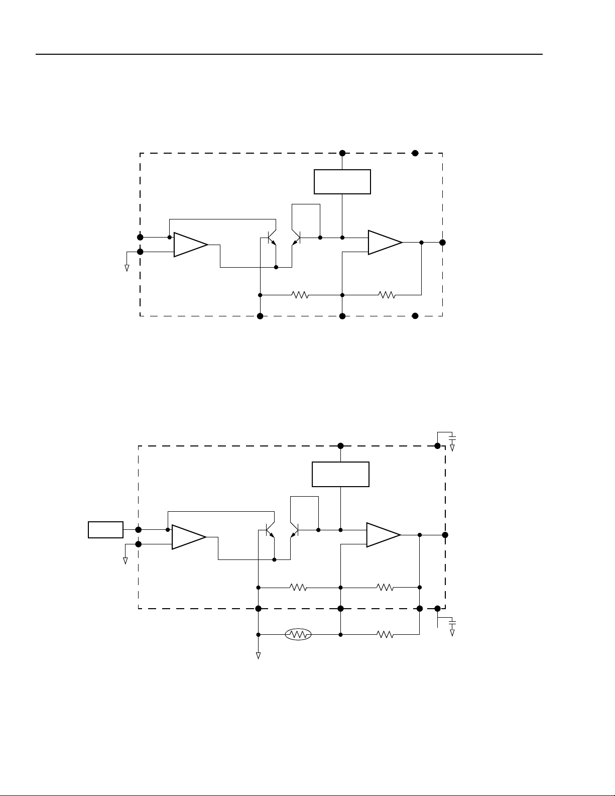
Block Diagram
OS_ADJ
V
IN (1)
(8)
CC (5)
REF_ADJ
I
REFERENCE
IN–
V
(3)
CURRENT
V
IN+
V
OUTPUT (6)
IN–
IN+
V
V
10.2 k 160 kΩΩ
V
GND (2)
SCALE FACTOR (7)
EE
(4)
2352.a(F)
Figure 1. LSP2961 Internal Block Diagram
Typical Application Circuit
IN–
V
IN+
V
V
OS_ADJ
PIN
(8)
GND (2)
V
CC
REF_ADJ
I
REFERENCE
CURRENT
(3)
IN+
V
IN–
V
10.2 k 160 kΩΩ
SCALE FACTOR (7)
EE
V
1 k
(0.42%)
THERMISTOR
16 kΩΩ
RESISTOR
µ0.1 F
OUTPUT (6)
µ0.1 F
2353.b(F)
Figure 2. Typical Application Circuit with External Temperature Compensation
2 Agere Systems Inc.
 Loading...