

AGERE LSP2916B, LSP2916A Datasheet
LSP2916 16-Channel, High-Voltage Driver
Preliminary Data Sheet
July 2001
Features
■
16 amplifier channels available in one package.
■
Outputs from 0 V to –298 V per channel.
■
Programmable output current limit (50 µA to
300 µA).
■
Fixed gain set by internal resistors. (The fixed gain
for version A is –32 V/V, and –66 V/V for version
B.)
■
Minimal external components.
Applications
■
Optical crosspoint switches.
■
Optical microelectromechanical systems (MEMS)
components.
Description
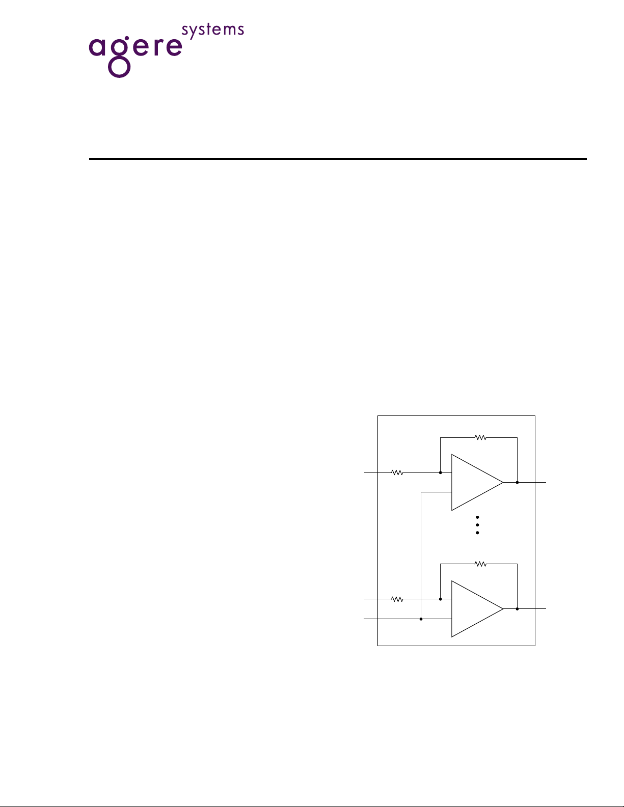
This LSP2916 16-channel, high-voltage (HV) driver
is targeted for microoptomechanical systems. Each
device contains 16 high-voltage amplifiers with an
output voltage range of 0 V to –298 V. Internal gainsetting resistors provide a fixed gain of –32 V/V,
thereby minimizing external component count. Each
amplifier can output up to 300 µA, ideal for deflection
and control of optical MEMS mirrors. Output current
limit is programmed by an external resistor.
Additionally, careful attention was paid to minimizing
offset drift and gain variation over temperature. The
internal block diagram is shown in Figure 1. There
are two versions, version A (LSP2916A) and version
B (LSP2916B). For version A, R
RIN
= 250 kΩ; and for version B, RF = 8.25 MΩ and
RIN
= 125 kΩ. So LSP2916A has the fixed gain of
–32 V/V and LSP2916B has the fixed gain of
–66 V/V.
F
= 8 MΩ and
The LSP2916 requires one negative high-voltage
power supply (V
power supply (V
HN
) and one positive 5 V analog
LP
). Corresponding to the 16
channels, there are 16 negative input voltage pins,
–INx (x = 1, 2, . . . , 16), and the corresponding 16
output pins, OUTPUTx
(x = 1, 2, . . . , 16).
+IN is the noninverting input for all 16 amplifiers,
which means all the amplifiers share the same
noninverting input. +IN should be connected to GND
for typical applications. I
BIAS
pin will set the current
limit for the amplifiers by connecting it to an external
resistor. The LSP2916 is available in a leaded
surface-mount 64-pin MQFP package.
Block Diagram
LSP2916
R
–IN1
–IN16
+IN
IN
R
IN
Figure 1. LSP2916 Internal Functional Block
Diagram
R
F
–
+
R
F
–
+
OUTPUT 1
OUTPUT 16
1682(F)
LSP2916 16-Channel, High-Voltage Driver
Preliminary Data Sheet
July 2001
Description
(continued)
Typical Application Circuit
DAC
–IN1
LSP2916
RIN
0.1 µF
10 Ω
HN
V
0.1 µF
LP
V
F
R
–
+
F
R
OUTPUT 1
MEMS
MATRIX
DAC
–IN16
+IN
IN
R
GND
–
+
Rib = 143 kΩ
Figure 2. Typical Application Circuit
OUTPUT 16
1683(F)
22 Agere Systems Inc.
Preliminary Data Sheet
July 2001
Pin Information
NC
–IN9
–IN10
–IN11
–IN12
NC
NC
NC
NC
NC
NC
–IN5
–IN6
–IN7
–IN8
NC
LSP2916 16-Channel, High-Voltage Driver
NC
OUTPUT14
NC
OUTPUT13
NC
OUTPUT12
NC
OUTPUT11
NC
OUTPUT10
NC
OUTPUT9
53
54
55
56
57
58
59
60
61
62
63
64
1
2
3
4
5
6
7
8
9
10
11
12
13
14
15
16
171819202122232425262728293031
OUTPUT16
NC
NC
OUTPUT15
49
50
51
52
48
NC
47
–IN16
46
–IN15
45
–IN14
44
–IN13
43
+IN
42
NC
41
NC
40
BIAS
I
39
VLP
38
GND
37
–IN4
36
–IN3
35
–IN2
34
–IN1
33
NC
32
HN
V
OUTPUT8NCOUTPUT7NCOUTPUT6NCOUTPUT5NCOUTPUT4NCOUTPUT3NCOUTPUT2NCOUTPUT1
Figure 3. External Connections
Table 1. LSP2916 Pin Order
Pin
Number
Symbol Pin
Number
Symbol Pin
Number
Symbol Pin
Number
Symbol
1 NC 17 OUTPUT8 33 NC 49 OUTPUT16
2–IN918 NC 34–IN150 NC
3 –IN10 19 OUTPUT7 35 –IN2 51 NC
4 –IN11 20 NC 36 –IN3 52 OUTPUT15
5 –IN12 21 OUTPUT6 37 –IN4 53 NC
6 NC 22 NC 38 GND 54 OUTPUT14
7NC23OUTPUT539V
8NC24NC40I
LP
BIAS
55 NC
56 OUTPUT13
9 NC 25 OUTPUT4 41 NC 57 NC
10 NC 26 NC 42 NC 58 OUTPUT12
11 NC 27 OUTPUT3 43 +IN 59 NC
12 –IN5 28 NC 44 –IN13 60 OUTPUT11
13 –IN6 29 OUTPUT2 45 –IN14 61 NC
14 –IN7 30 NC 46 –IN15 62 OUTPUT10
15 –IN8 31 OUTPUT1 47 –IN16 63 NC
16 NC 32 V
HN
48 NC 64 OUTPUT9
1541.a(F)
Agere Systems Inc. 3
 Loading...