

AGERE LH1465AB, LH1465AAE Datasheet
Advisory
July 1998
LH1465AB/AAE ISDN dc Termination IC
Data Sheet Advisory
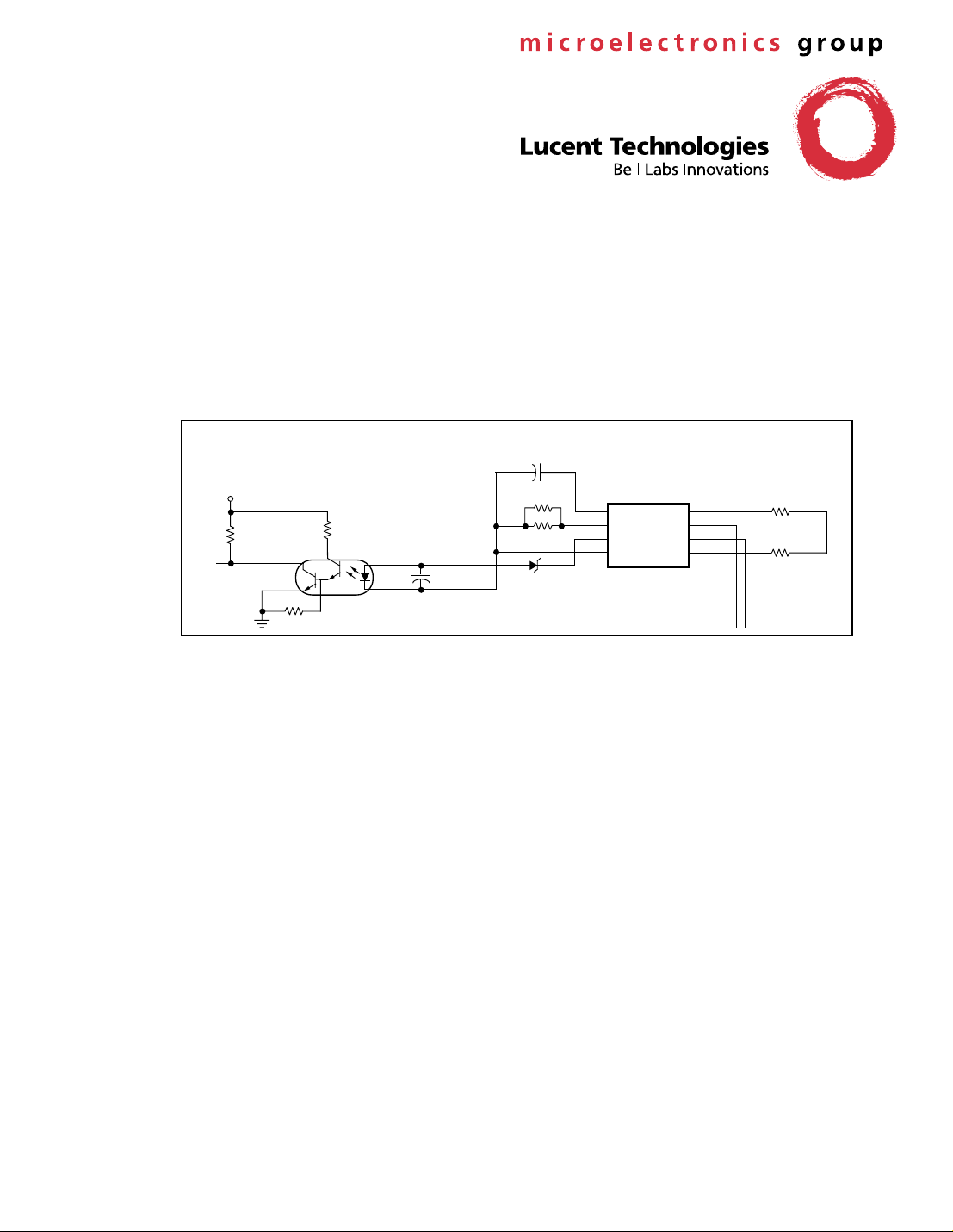
Application Circuit
Replace Figure 11 on page 10 of the LH1465AB/AAE data sheet with the figure shown below.
+5 V
SCNT1
OPTOIN
PIN
R8
17.8 kΩ
10 kΩ
6
5
R9
2.2 MΩ
R10
8
7
MLT CIRCUIT
U2
2
3
HCPL-0701
CA
1.0 µF
C15
1.0 µF
FOR NORTH AMERICAN
APPLICATIONS ONLY
(PLACE THIS CAPACITOR AS
CLOSE AS POSSIBLE TO THE LH1465)
R11
137 Ω
R12
137 Ω
ZD
8
TC
7
RS
6
PD
5
COM
LH1465AB
U3
PR+
PR–
T
R
1
2
3
4
RING TIP
R14
1.1 kΩ
2 W
R15
1.1 kΩ
2 W
5-7034(C)
Figure 1. MLT Circuit Showing New Placement of Zener Diode (ZD) and Capacitor (CA)
In the ILOSS mode (refer to ANSI T1.601 1992, Section 6.5.2), the NT generates a scrambled, framed, 2B1Q
signal such as SN1 and SN2. When the ILOSS mode is applied to circuits with the LH1465, it was observed
that for some short loop lengths, the NT, once in the ILOSS mode, would not respond to further maintenance
pulses until the ILOSS timer expired. It was discovered that there is some portion of the transmitted 2B1Q signal from the NT that passes through the LH1465 to the optoisolator. This causes the optoisolator to report
incorrect dial pulses at its output, and thus prevent the NT from properly exiting the ILOSS mode.
To correct this situation, the dropout voltage (voltage at the Tip/Ring needed to turn on the optoisolator) of the
optoisolator driver on the LH1465 is raised using the 3.6 V zener diode Z
MMSZ4685T1). Capacitor C
is a 1.0 µF ±10% tantalum chip capacitor, with a voltage rating of at least 16 V.
A
(for example,
D
Motorola
*
CA is added to provide a level of filtering for the transition points (turn-on or turn-off) of the optoisolator input
voltage, which increases the robustness of the circuit.
*
Motorola
is a registered trademark of Motorola Inc.

For additional information, contact your Microelectronics Group Account Manager or the following:
INTERNET:
E-MAIL:
N. AMERICA: Microelectronics Group, Lucent Technologies Inc., 555 Union Boulevard, Room 30L-15P-BA, Allentown, PA 18103
ASIA PACIFIC: Microelectronics Group, Lucent Technologies Singapore Pte. Ltd., 77 Science Park Drive, #03-18 Cintech III, Singapore 118256
CHINA: Microelectronics Group, Lucent Technologies (China) Co., Ltd., A-F2, 23/F, Zao Fong Universe Building, 1800 Zhong Shan Xi Road,
JAPAN: Microelectronics Group, Lucent Technologies Japan Ltd., 7-18, Higashi-Gotanda 2-chome, Shinagawa-ku, Tokyo 141, Japan
EUROPE: Data Requests: MICROELECTRONICS GROUP DATALINE:
Lucent Technologies Inc. reserves the right to make changes to the product(s) or information c ontained herein without notice. No liability is assumed as a result of their use or application. No
rights under any patent accompany the sale of any such product(s) or information.
Copyright © 1998 Lucent Technologies Inc.
All Rights Reserved
Printed in U.S.A.
July 1998
AY98-028ISDN (Replaces AY98-013ISDN)
http://www.lucent.com/micro
docmaster@micro.lucent.com
1-800-372-2447
Tel. (65) 778 8833
, FAX 610-712-4106 (In CANADA:
, FAX (65) 777 7495
Shanghai 200233 P. R. China
Tel. (81) 3 5421 1600
Technical Inquir ies: GERMANY:
, FAX (81) 3 5421 1700
FRANCE:
(39) 2 6601 1800
IT ALY:
1-800-553-2448
Tel. (86) 21 6440 0468, ext. 316
(49) 89 95086 0
(33) 1 48 83 68 00
(Munich), UNITED KINGDOM:
(Paris), SWEDEN:
(Milan), SPAIN:
, FAX 610-712-4106)
, FAX (86) 21 6440 0652
Tel. (44) 1189 324 299
(46) 8 600 7070
(34) 1 807 1441
(Madrid)
, FAX (44) 1189 328 148
(44) 1344 865 900
(Stockholm), FINLAND:
(Bracknell),
(358) 9 4354 2800
(Helsinki),
(Must accompany DS97-414ISDN)
Data Sheet
February 1998
LH1465AB/AAE ISDN dc Termination IC
Features
■
ANSI U-DSL compatible
■
High linearity
■
MLT compatible
■
SARTS compatible
■
Portable test set compatible
Device Code Package Type
LH1465AB 8-Pin, Plastic DIP
LH1465AAE 16-Pin, Plastic SOG
2
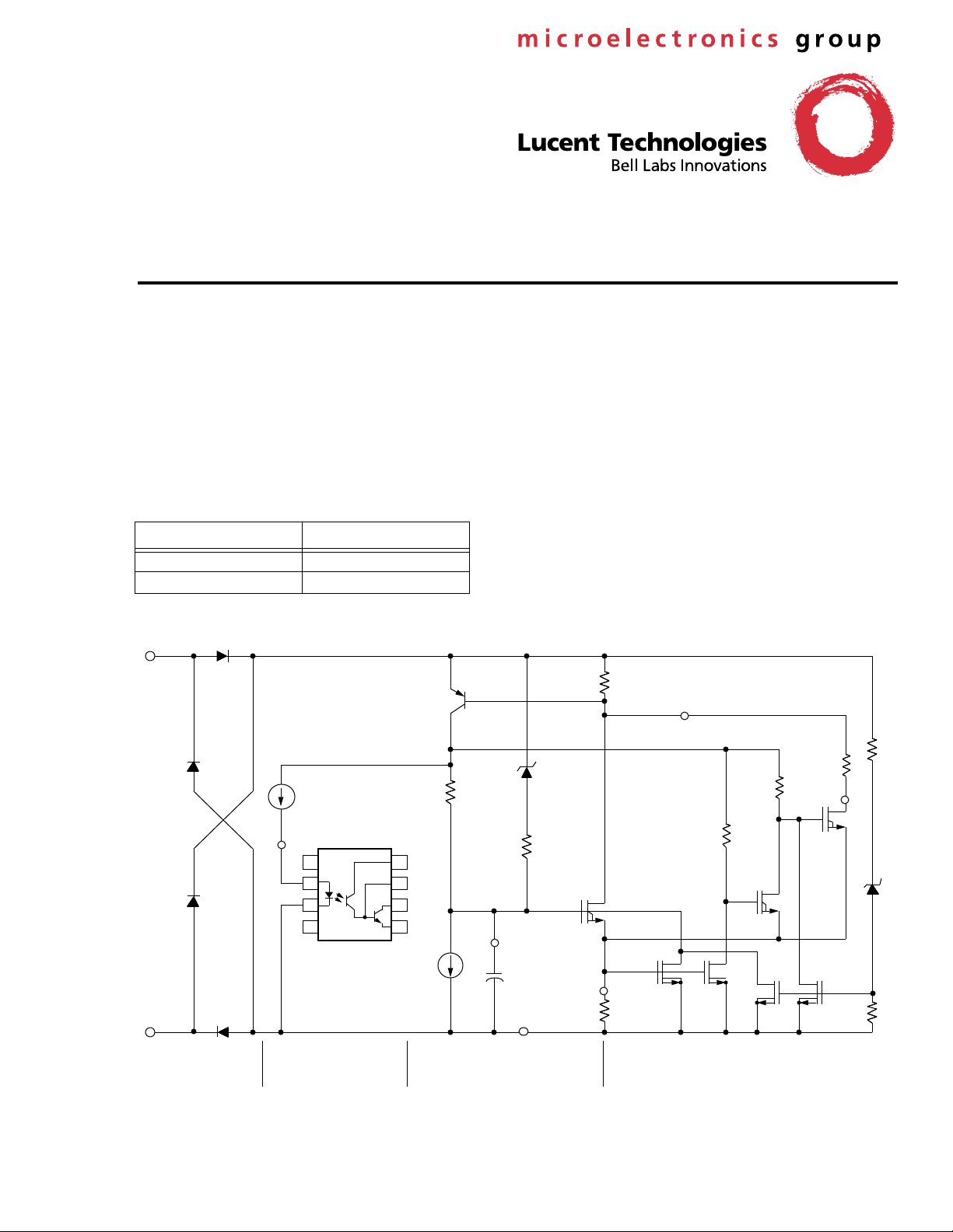
Description
The LH1465 ISDN dc Termination IC is used on Uinterface digital subscriber lines (U-DSL) and provides a polarity insensitive dc termination for the
loop-sealing current and a recognizable signature for
mechanized loop testing (MLT) systems. The LH1465
passes dc signaling information to the NT1 circuitry
through a 6N139 optoisolator (or equivalent). The
LH1465 IC consists of two functional blocks. The first
provides the electronic inductor and silicon-controlled
rectifier portion of the termination, while the second
drives the LED of the 6N139 optoisolator. Inquire
about the availability of tape-and-reel packaging for
the 16-pin SOG (LH1465AAE).
1
2.2 kΩ
4 W, 5%
4
3
POLARITY
GUARD
6
OPTOISOLATOR
PD1
1
2
3
45
6N139
DRIVER
8
7
6
Figure 1. Functional Diagram/8-Pin DIP
8
1 µF
15 V, 10%
1/4 W, 1%
5
ELECTRONIC INDUCTOR,
BREAKOVER, AND
LATCH CIRCUITS
7
68 Ω
CURRENT LIMIT AND EXCESS
POWER PROTECTION
12-1947(F)
*
LH1465AB/AAE ISDN dc Termination IC
Functional Description
The LH1465 plays a dual role in the ISDN NT1: first, as
an electronic inductor for a dc termination with high ac
impedance; and second, as part of the dc signaling
system for line testing capability. The LH1465 meets or
exceeds all specifications for the ISDN NT1 dc termination as described by ANSI Standard T1.601-1991.
Use of the LH1465 requires only a few discrete components. See Figure 11 for a typical NT1 application. The
LH1465 is current limited, but is not an overvoltage
surge protector. A crowbar-type surge protector limiting
the line voltage to less than 250 V is recommended to
protect the LH1465. The surge protector must withstand the requirements in Tables 4 and 5. One such
protector is the Teccor * Inc., P2000AA61 SIDACTOR *.
The LH1465 has a polarity guard so that the device
gives the same characteristics whether the NT1 TIP or
RING terminal is connected to the battery voltage. TIP
and RING are connected directly to the LH1465AB
terminals 2 and 3 and to the LH1465AAE terminals 4
and 5.
The dc T to R I-V characteristics of the LH1465 are
shown in Figures 2 and 3. As battery voltage is applied
to the loop, the LH1465 conducts current only when the
voltage across the LH1465 exceeds about 35 V. With
35 V or more applied to the LH1465A, the device conducts about 150 µ A of current for about 20 ms and then
turns on and goes into the ON state. The LH1465 will
remain in the ON state for as long as the loop current
exceeds 0.5 mA.
The LH1465 has a turn-on and turn-off timing circuit
that ensures that the LH1465 will: a) not turn on if a
voltage above 43.5 V is applied for less than 3 ms; and
b) not turn off if the loop current is interrupted for less
than 3 ms.
Current for the LED of the optocoupler flows when the
current in the LH1465 is greater than 1 mA. However,
the LH1465 is guaranteed to turn on if a voltage above
43.5 V is applied for more than 50 ms, and turn off if
Data Sheet
February 1998
1 mA loop current is interrupted for more than 100 ms.
See Figures 6, 7, and 8 of this document or Table F1 in
Appendix F of ANSI Standard T1.601-1991.
Current for the LED is interrupted when loop current is
interrupted. The current in the ON state is determined
by the battery voltage and loop resistance. Should the
loop resistance be negligible and/or applied voltage
excessively large , the LH1465 will limit the loop current
to less than 60 mA. While in current limit, the LH1465
shunts the 2.2 k Ω , 4 W power resistor R2 across itself
to protect against excessive thermal heating.
In the event that fault voltages exceeding 100 V are
impressed upon TIP and RING, the LH1465 will shut
off and go into a standby mode where very little current
flows. When the fault voltage is removed, the LH1465
goes back into its normal ON-state operation.
Pin Descriptions
DIP SOG Symbol Name/Function
1 1 PR+ Protection resistor positive
side
2 4 T Tip side of the loop
3 5 R Ring side of the loop
4 8 PR– Protection resistor negative
side
5 9 COM Common
6 12 PD Photodiode (LED input
current)
7 13 RS Current-limit resistor
8 16 TC Timing capacitor
2, 3 NC No connection
6, 7 NC No connection
10, 11 NC No connection
14, 15 NC No connection
Teccor is a trademark and SIDACTOR is a registered trademark of Teccor, Inc.
22 Lucent Technologies Inc.
Data Sheet
February 1998
°
°
°
≤
µ
≤
≤
≤
≤
LH1465AB/AAE ISDN dc Termination IC
Absolute Maximum Ratings
At 25 ° C
Stresses in excess of the absolute maximum ratings can cause permanent damage to the device. These are absolute stress ratings only. Functional operation of the device is not implied at these or any other conditions in excess
of those indicated in the operations sections of the data sheet. Exposure to absolute maximum ratings f or e xtended
periods can adversely affect device reliability.
Parameter Symbol Min Typ Max Unit
Ambient Operating Temperature T
Storage Temperature T
Power Dissipation P
Pin Soldering Temperature (t = 15 s) — — — 300
A
stg
–40 — 85
–40 — 125
D
—— 1 W
C
C
C
Maximum Voltage (T/R, R/T)* — — — 300 Vdc
* If the SOG package is used, it is recommended to place a drop of RTV (room temperature vulcanizing) compound on the tip and ring pins
(pins 3 and 4). This will guard against the possibility of arcing between the pins (which are 0.030 in. apart) under worst-case dust and oil
board buildup conditions.
T
= 25 ° C
Electrical Characteristics
A
Minimum and maximum values are testing requirements. Typical values are characteristics of the device and are
the result of engineering evaluations. Typical values are for information purposes only and are not part of the testing requirements.
Table 1. dc Specifications, Normal Operation (See Figures 2 and 3.)
Parameter Symbol Test Condition Min Typ Max Unit
Activate/Nonactivate Voltage V
Breakover Current I
dc Voltage Drop Active State V
dc Leakage Current I
Hold/Release Current Active
BO
LKG
I
H/R
AN
ON
1 mA ≤ I
V
OFF
— 30.0 37.0 39.0 V
— — 0.5 1.0 mA
SL
20 mA — 13.75 15 V
= 20 V — 0.001 5
— 0.1 0.5 1.0 mA
State
Minimum ON Current I
Minimum ON Current I
MIN1
MIN2
54 V ≤ V
ON
V
< 54 V 20 35 — mA
ON
100 V f or 2 s Source
9.0 45 — mA
Resistance: 200 Ω to 4 k Ω
Minimum ON Current I
Maximum ON Current I
Maximum ON Current I
Optocoupler LED Current
MIN3
MAX1
MAX2
I
LED
V
> 100 V 0 0.2 — mA
ON
V
70 V — — 70 mA
ON
V
> 70 V — — mA
ON
— 0.2 0.3 10 mA
Active State (6N139)
Table 2. ac Specifications, Normal Operation
Parameter Symbol Test Condition Min Typ Max Unit
ac Impedance Z
Linearity Distortion D
Linearity Distortion D
MT
200 Hz to 50 kHz (See Figure 4.) 10 50 — k Ω
1
2
f = 200 Hz to 40 kHz, I
APP
V
10.5 V
PP
f = 200 Hz to 40 kHz, I
V
12 V
APP
PP
SL
= 1 mA to 20 mA
(See Figures 4 and 5.)
SL
= 1 mA to 20 mA
(See Figures 4 and 5.)
75 84 — dB
50 80 — dB
VON
------------- -
1 kΩ
A
Lucent Technologies Inc. 3
 Loading...