

AGERE LG1628AXA Datasheet
Preliminary Data Sheet
January 1998
LG1628AXA SONET/SDH 2.488 Gbits/s
Transimpedance Amplifier
Features
■
High data rate: 2.5 Gbits/s
■
High gain: 5.8 k Ω transimpedance
■
Complementary 50 Ω outputs
■
Low noise
■
Ultrawide dynamic range
■
Single –5.2 V ECL power supply
Applications
■
SONET/SDH receivers
■
SONET/SDH test equipment
■
Digital video transmission
Functional Description
The Lucent Technologies Microelectronics Group
LG1628AXA is a hybrid integrated circuit that combines the Lucent LG1628A gallium arsenide (GaAs)
transimpedance amplifier chip with an external Si
dual operational amplifier and necessary filtering to
achieve an ultrawide dynamic range amplifier. The
LG1628AXA is capable of handling input currents
from 3 µ A
avg
to 4 mA
operation is from a single –5.2 V power supply. The
targeted transmission system is SONET OC-48 and
SDH STM-16.
avg
(patent pending). Amplifier
A complete receiver/regenerator can be constructed
with an LG1628AXA followed by an LG1605 limiting
amplifier and LG1600 clock and data regenerator.
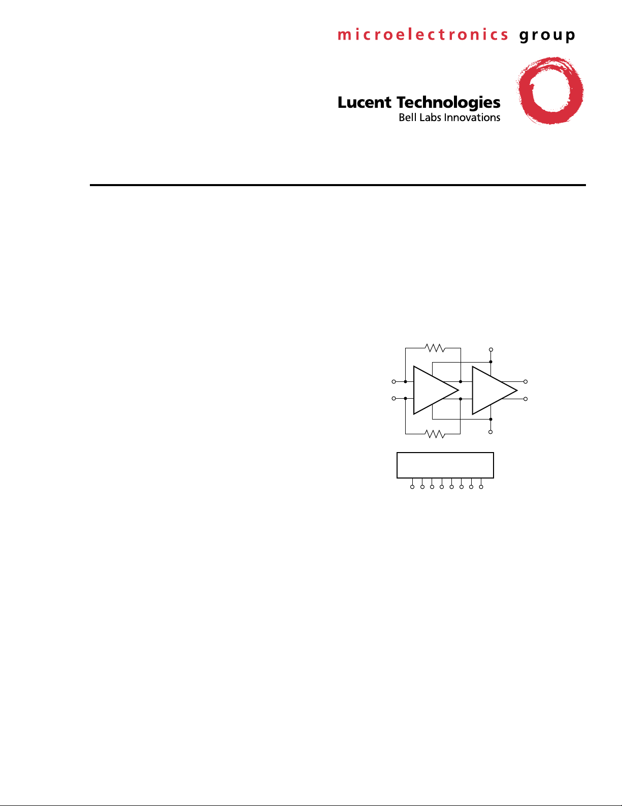
Figure 1 shows the block diagram of the LG1628AXA
transimpedance amplifier. The amplifier consists of a
4.2 k Ω differential transimpedance stage followed by
a limiting buffer that provides complementary 50 Ω
outputs.
IN–
IN+
ZEFF
OVERLOAD CONTROL
RF
F
R
GND
V
SS
OUT+
OUT–
50 Ω
LIMITING
BUFFER
5-5329(F)
Figure 1. LG1628AXA Functional Diagram
LG1628AXA SONET/SDH 2.488 Gbits/s Preliminary Data Sheet
Transimpedance Amplifier January 1998
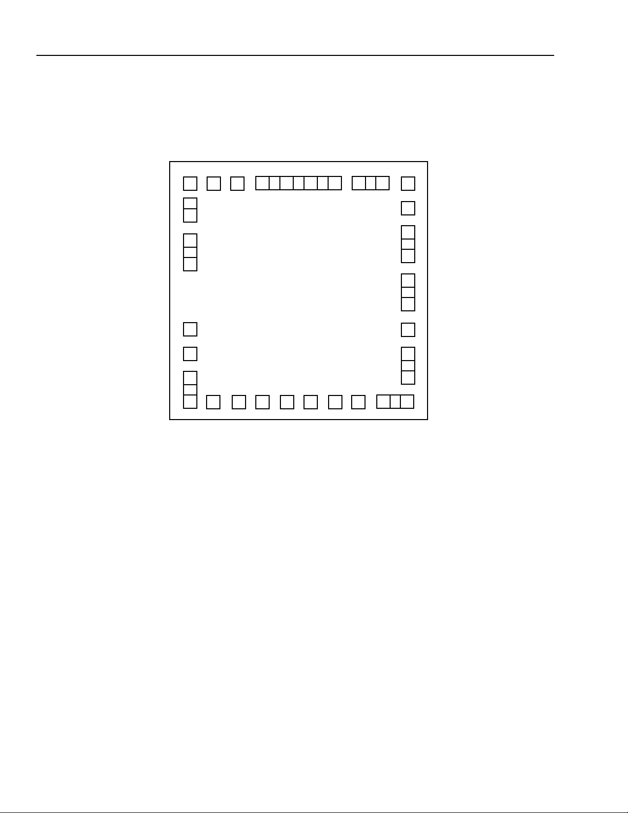
Die Pad Configuration
The die pad configuration is shown in Figure 2.
DNC
GND1
IN–
IN+
GND1
BYPASS
DNC
DNC
23
24
24
OUTSIDE DIE DIMENSIONS:
1.62 mm
PAD SIZE:
100 µm2 x 100 µm
(EXCEPT PAD #23, 100 µm2 x 150 µm2)
PAD SEPARATION:
50 µm
1
2
3
4 5 6 7 8 9 10 11 11
3
OP2OUT
OUT
OP1
2
x 1.62 mm
OP1–
GND1
2
OP1+
2
OP2–
OP2+A
GND2
OP2+B
VSS1
17181819191919202122
16
15
15
14
14
13
12
12
BG
GND2
OUT+
OUT–
GND2
VSS2
5-5336(F)r.2
Figure 2. Die Pad Configuration
2
Lucent Technologies Inc.

Preliminary Data Sheet LG1628AXA SONET/SDH 2.488 Gbits/s
January 1998 Transimpedance Amplifier
Die Pad Configuration
(continued)
The pad descriptions for the LG1628AXA are given in Table 1.
Table 1. Pad Descriptions
Pad Symbol Description
1 IN+ Amplifier input; connect to detector anode, current should enter this node.
2, 19, 23 GND
1
Ground.
3 BYPASS Connections between these nodes and an external dual op amp form the over4 OP2
5 OP1
OUT
OUT
6 OP1–
load control circuitry. See the test circuit in Figure 4 for wiring details.
To operate the amplifier without overload control connect OP2
OP1
OUT
to GND, and leave BYPASS and the remaining op amp connections
OUT
to V
open (Figure 5).
7 OP1+
8 OP2–
9 OP2+A
10 OP2+B
11 V
12 V
13, 16, 18 GND
SS1
SS2
Supply voltage; –5.2 Vdc nominal.
Supply voltage; –5.2 Vdc nominal.
2
Ground.
14 OUT– Inverted data output (produces low-level output for current entering IN+).
15 OUT+ Noninverted data output (produces high-level output for current entering IN+).
17 BG Connection for external –2.5 Vdc voltage reference (typically use an Si band-
gap).
20, 21, 22 DNC Do not connect; internal test point or reserved for future use.
24 IN– Inverting input; must provide ac bypass to ground when using overload control.
SS
,
Lucent Technologies Inc.
3
LG1628AXA SONET/SDH 2.488 Gbits/s Preliminary Data Sheet
Transimpedance Amplifier January 1998
Typical Connections and Padout of the Hybrid Integrated Circuit
APD
IN+
APD+
17
16
8
60x30
60x30
OUT+*
50 Ω
7
14
2
5
60x30
18
15
13
60X30
60X30
12
3
120X100
OUT–*
50 Ω
109
60x30
6
20
4
125x60
19
60X30
+VDET VSS
GND THERMISTOR
5-5336(F).r3
* OUT– is delayed approximately 25 ps with respect to OUT+ due to the longer microstrip line associated with OUT–. An extra delay should be
added to OUT+ before connecting to the next circuit.
Figure 3. Typical Connections to the HIC (See Figure 4 for a Schematic of the Circuitry on the HIC.)
Table 2. HIC Pad Functional Description
Symbol Description
IN+ Amplifier input; connect to detector anode, current should enter this node.
APD+ RF bypassed connection for the cathode of the APD.
+V
V
DET
SS
APD power supply connection.
Supply voltage; –5.2 Vdc nominal.
GND Ground (back of HIC is also ground).
Thermistor Negative temperature coefficient thermistor for APD gain control.
OUT+ Noninverted data output (produces high-level output for current entering IN+).
OUT– Inverted data output (produces low-level output for current entering IN+).
4
Lucent Technologies Inc.
 Loading...