

AGERE LG1627BXC Datasheet
g
y
µm g
gy
g
g
y
y
j
g
y
g
ying
LG1627BXC Clocked Laser Driver
Data Sheet
May 2001
Features
■
High data-rate clocked laser diode driver
■
Clock disable mode for data feedthrough
■
Adjustable high output current
■
Operation up to 3 Gbits/s
Applications
■
SONET/SDH transmission systems
■
SONET/SDH test equipment
■
Optical transmitters
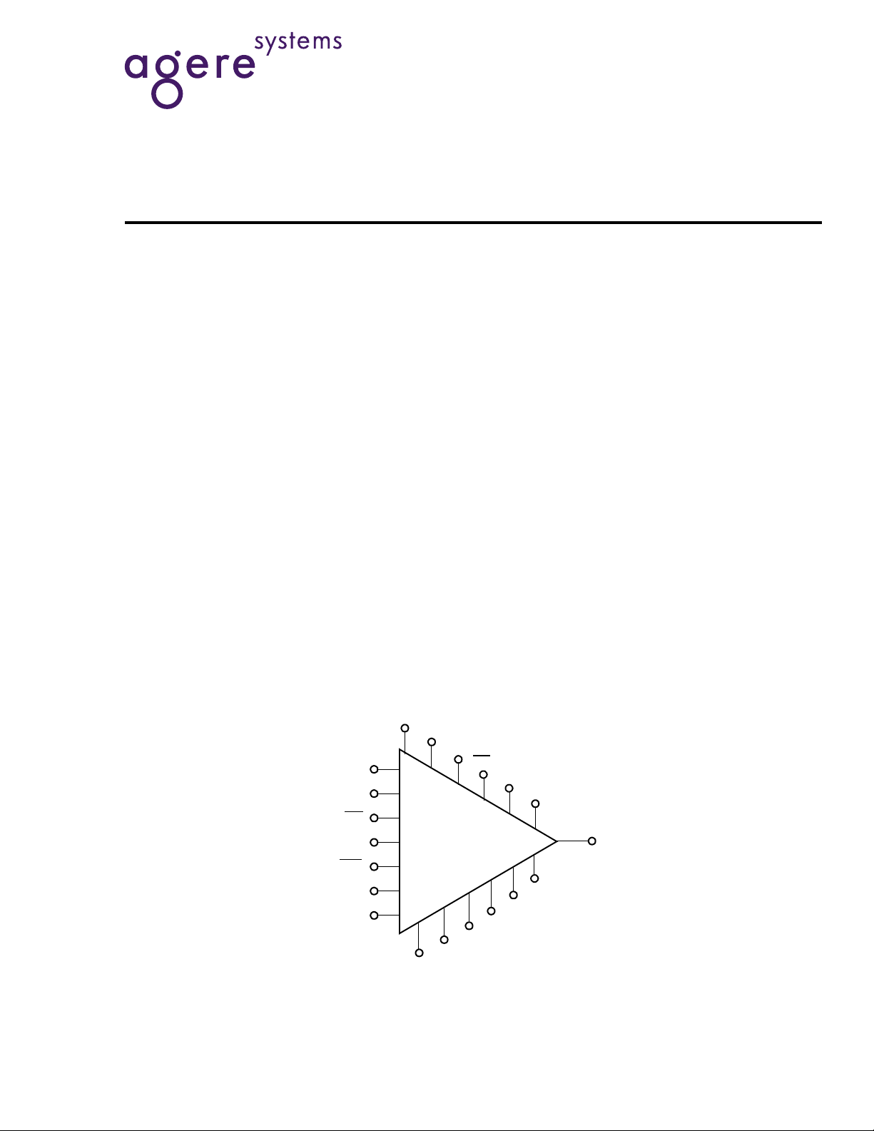
Functional Diagram
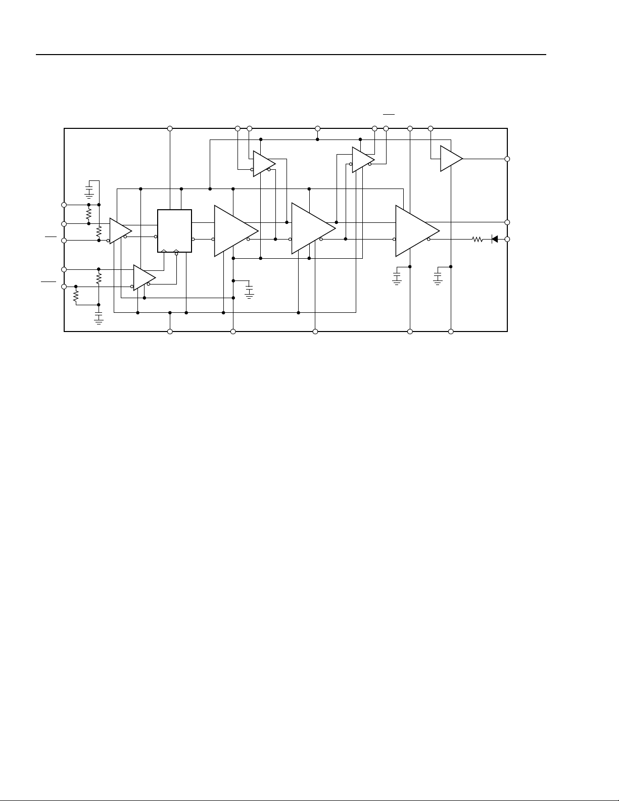
Functional Description
The LG1627BXC is a gallium arsenide (GaAs) laser
diode driver to be used with direct modulated laser
diodes in hi
mission s
performance 0.9
technolo
airbrid
tors. The driver includes differential data and clock
inputs. The hi
and prebias can be set separatel
accomplished b
itter on the data. Clocking can be disabled for data
feedthrou
to compensate for laser turn- on del a
ap reference is required for stable operation over
temperature and var
h-speed non-return-to-zero (NRZ) trans-
stems. The device is made in a high-
ate GaAs hetero-junction FET
that utilizes high-density MIM capacitors,
e interconnect, and NiCr film precision resis-
h-output, low overshoot drive current
. Data retiming is
the internal flip-flop, minimizing
h. A pulse-width control enables the user
. A 2.5 V band-
power supply voltage.
GND
BG2P5
MK
PWN
MK
PRE
V
OUT-PRE
I
OUT
I
MOD
V
SS3
V
SS2
V
SS1
V
5-6549(F).b
TH
V
V
V
CLK
CLK
CLK_E
MOD_E
IN
IN
LG1627BXC
PWP
Figure 1. Functional Diagram
LG1627BXC Clocked Laser Driver
Block Diagram
V
TH
50
V
V
Ω
IN
50
IN
Ω
DQ
Data Sheet
May 2001
V
V
MKMKGNDPWNPWPCLK_E
MOD
PRE
22
I
OUT-PRE
I
OUT
Ω
GND
CLK
CLK
50
50
Ω
Ω
BG2P5 MOD_E V
V
SS1
SS3
V
SS2
5-7675(F)r.1
Figure 2. Block Diagram
2 Agere Systems Inc.
Data Sheet
y
g
g
g
g
(
(
j
j
y
(
May 2001
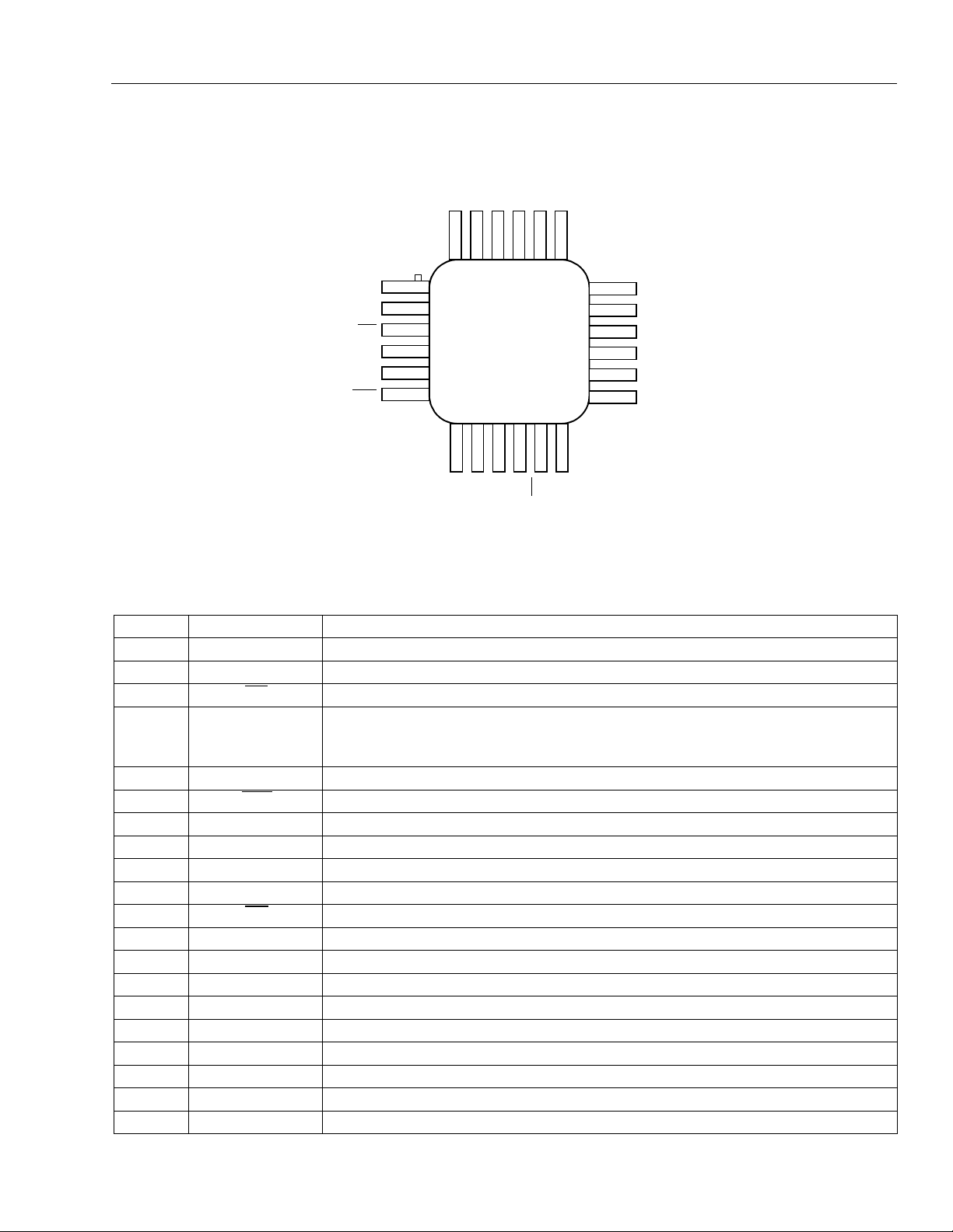
Pin Information
TH
V
V
V
GND
CLK
CLK
LG1627BXC Clocked Laser Driver
SS2
SS3
MODVSS1
SS1
V
CLK_EBG2P5
1
IN
IN
2
3
4
5
6
7 8 9 10 11 12
PWP
MOD_E
Figure 3. Pin Diagram
V
PWN
V
MK
V
192021222324
PRE
18
17
16
15
14
13
MK
V
OUT-PRE
I
OUT
I
OUT
I
GND
GND
5-6551(F).br.3
Table 1. Pin Descriptions
Pin Symbol Description
1V
2V
3 Complementar
4, 13, 14,
packa
e
TH
IN
IN
V
Capacitor to ground (data input reference).
Data input.
data input.
GND Ground. For optimum performance, the packa
round plane.
bottom
5 CLK Clock input.
6CLK
7BG2P5−2.5 V band8 MOD_E Modulation enable
9 PWP Pulse width ad
10 PWN Pulse width ad
11 MK
12 MK Mark densit
15, 16 I
17 I
18 V
19 V
20 V
21 V
22, 23 V
OUT
OUT-PRE
PRE
SS2
SS3
MOD
SS1
24 CLK_E Clock enable
Complementary clock input.
ap reference
connect to V
National Semiconductor
SS1
to enable, float to disable).
ust positive.
ust negative.
Complementary mark density output.
output.
Output modulation current (dc coupled to laser cathode).
Output prebias current.
Prebias control input.
SS2
V
supply −5.2 V for output prebias.
SS3
V
supply −5.2 V for output modulation.
Modulation current control input.
SS1
V
supply −5.2 V.
connect to V
SS1
to enable, float to disable).
e bottom must be soldered to the
* p/n LM4040).
National Semiconductor
*
is a registered trademark of National Semiconductor Corporation.
Agere Systems Inc. 3
 Loading...