

AGERE LG1626DXC Datasheet

Data Sheet
February 1999
LG1626DXC Modulator Driver
Features
■
High data-rate optical modulator driver
■
Adjustable output voltage up to 3 Vp-p (RL = 50 Ω)
■
Adjustable modulator dc offset
■
Operation up to 3 Gbits/s
■
Single ended or differential inputs
■
Single –5.2 V power supply
■
90 ps rise and fall times
■
Enable control
Applications
■
SONET/SDM transmission systems
■
SONET/SDM test equipment
■
Optical transmitters
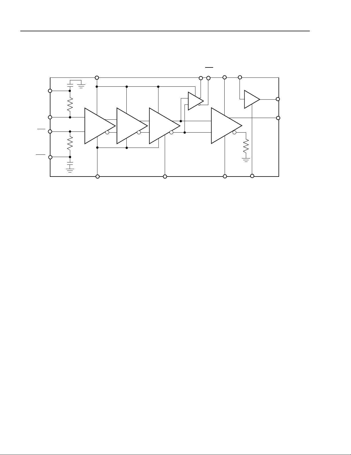
GND
BG2P5
TH
V
IN
V
Functional Description
The LG1626DXC is a gallium-arsenide (GaAs) intergrated circuit used to provide voltages to drive optical
modulators in high-speed non-return-to-zero (NRZ)
transmission systems. The device is made in a highperformance 0.9 µm gate GaAs hetero-junction FET
technology that utilizes high-density MIM capacitors,
airbridge interco nnec t, and NiCr film precis i on resi stors. The device contains four cascaded stages,
operates with a single –5.2 V power supply, and
accepts ECL 100K level inputs. The output is an
open drain designed to drive 50 Ω loads. Voltages
control the output modulation amplitude and modulator dc offset. A –2.5 V band-gap reference is required
for stable operation over temperature and varying
power supply voltage. The LG1626DXC is available
in a 24-lead hermetic, gull-wing package.
MK
MK
DC-ADJ
V
V
TH
V
MOD_E
IN
MOD
V
SS3
V
SS2
V
SS1
V
Figure 1. Functional Diagram
OUT
V
OUT-DC
V
5-6549(F)
LG1626DXC Modulator Driver
Pin Information
GND MKMK
TH
V
Ω
50
IN
V
IN
V
Ω
50
TH
V
Data Sheet
February 1999
MOD
50
DC-ADJ
V
Ω
V
OUT
V
+
–
+
–
SS1
V
MOD_E
SS3
V
SS2
V
5-6550(F)
Figure 2. LG1626DXC Die Block Diagram
2 Lucent Technologies Inc.
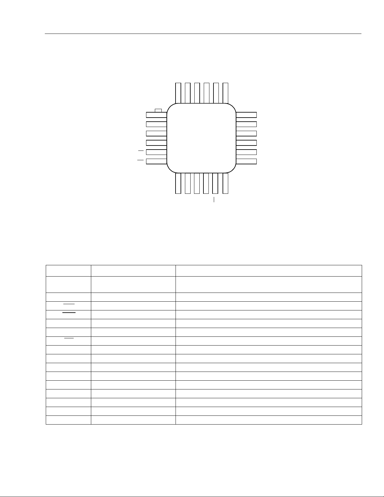
Data Sheet
February 1999
LG1626DXC Modulator Driver
Pin Information
Note: Figure is not to scale.
(continued)
GND
GND
GND
V
TH
V
V
24
23
1
IN
V
IN
V
TH
2
3
4
5
6
7
8
BG2P5
MOD_E
V
V
22
21
LG1626DXC
MODULATOR
DRIVER
9
10
GND
GND
V
20
11
MK
V
19
DC-ADJ
18
17
16
15
14
13
12
MK
V
OUT-DC
V
OUT
V
GND
GND
GND
5-6551(F)
SS2
SS3
MOD
SS1
SS1
Figure 3. LG1626DXC Package Pinout
Table 1. LG1626DXC Pin Description
Symbol Pin Description
GND 1, 3, 4, 9, 10, 13, 14, 15,
Package Bottom
V
--------- V
IN
----------V
TH
IN
2 Data input.
5 Complementary data input.
6 Complementary threshold control (eye crossing) input.
BG2P5 7 –2.5 V band-gap reference (
Ground. For optimum performance, the package bottom must be
soldered to the ground plane.
National Semiconductor
MOD_E 8 Modulation enable (connect to V
MK
MK
V
OUT
VOUT-DC
V
DC-ADJ
V
SS2
V
SS3
V
MOD
V
SS1
V
TH
11 Complementary mark density output.
12 Mark density output.
16 Output, ac couple to 50 Ω modulator.
17 Output, modulator dc offset.
18 Modulator dc offset control input.
19 V
20 V
supply –5.2 V for output prebias.
SS2
supply –5.2 V for output modulation.
SS3
21 Output modulation control input.
22, 23 V
supply –5.2 V.
SS1
24 Threshold control (eye crossing) input.
* LM4040).
to enable, float to disable).
SS1
National Semiconductor
*
is a registered trademark of National Semiconductor Corporation.
Lucent Technologies Inc. 3
 Loading...