

AGERE LG1625AXF Datasheet
Data Sheet
June 1999
LG1625AXF Laser Driver
Features
■
High data-rate laser diode/LED driver
■
Adjustable output current
■
Operation up to 3 Gbits/s
■
Single –5.2 V power supply
■
90 ps rise and fall times
Applications
■
SONET/SDH transmission systems
■
SONET/SDH test equipment
■
Optical transmitters
GND
MK
Description
The LG1625AXF is a gallium-arsenide (GaAs) laser
diode driver to be used with direct modulated laser
diodes in high-speed nonreturn-to-zero (NRZ) transmission systems. The device is made in a high-performance 0.9 µm gate GaAs heterojunction FET
technology that utilizes high-density MIM capacitors,
airbridge interconnect, and NiCr film precision resistors.
The device contains three cascaded stages, operates with a single –5.2 V power supply and accepts
ECL level inputs. Voltages control the modulated output current and laser prebias current. The
LG1625AXF is available in a 24-lead hermetic, gullwing package.
A test fixture (TF1006A) with SMA connectors is
available to allow quick evaluation of the LG1625AXF.
MK
PRE
V
IN
V
TH
V
LG1625AXF
SS1
V
SS3
V
SS2
V
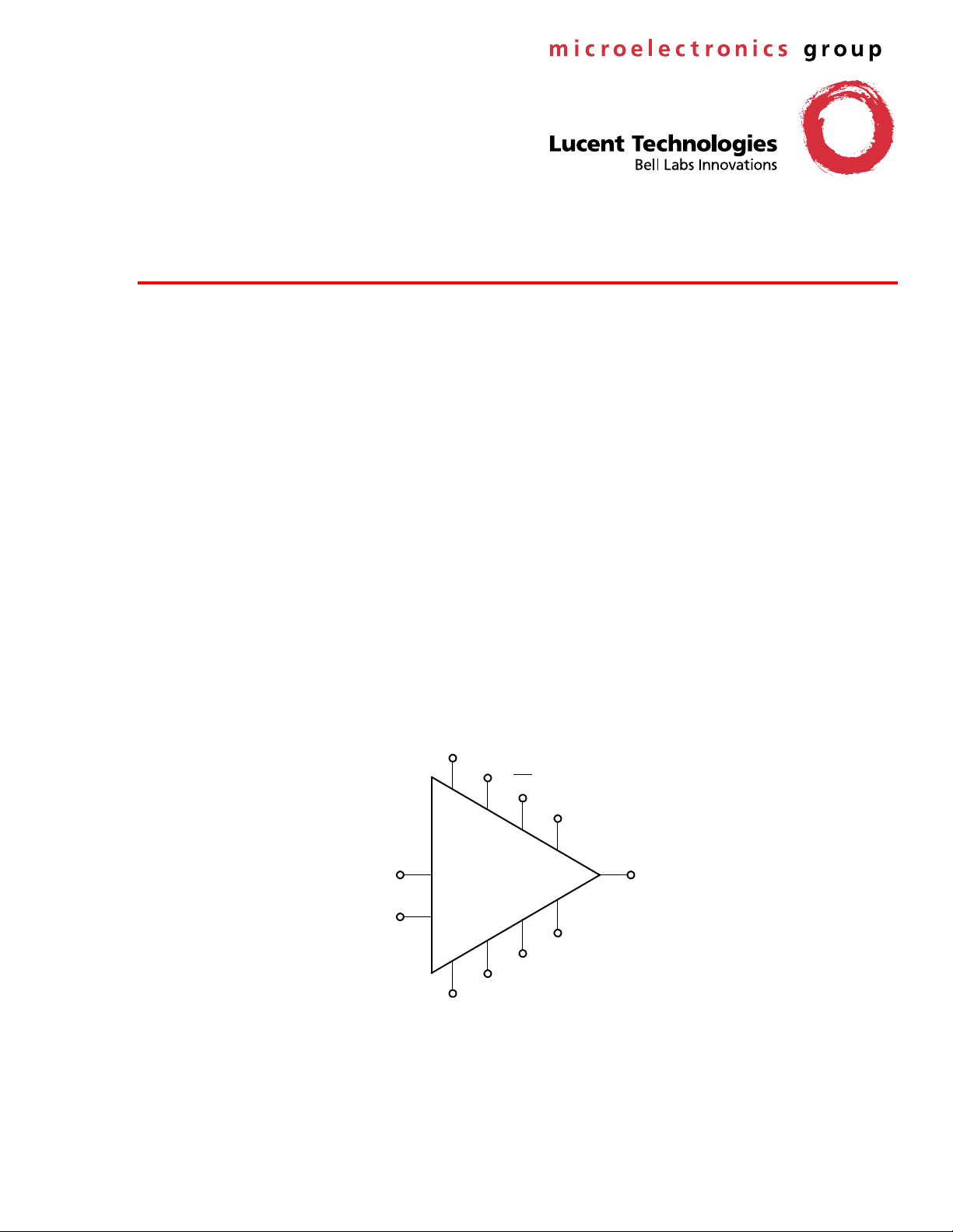
Figure 1. Functional Diagram
V
MOD
OUT
I
5-7865(F)
LG1625AXF Laser Driver
Pin Information
IN
V
Ω
50
TH
V
GND MKMK
+
–
+
–
V
+
–
MOD
Data Sheet
June 1999
PRE
V
OUT
I
Ω
25
SS1
V
V
GND
GND
GND
SS1
V
SS1
V
SS3
V
SS2
V
5-7866(F)
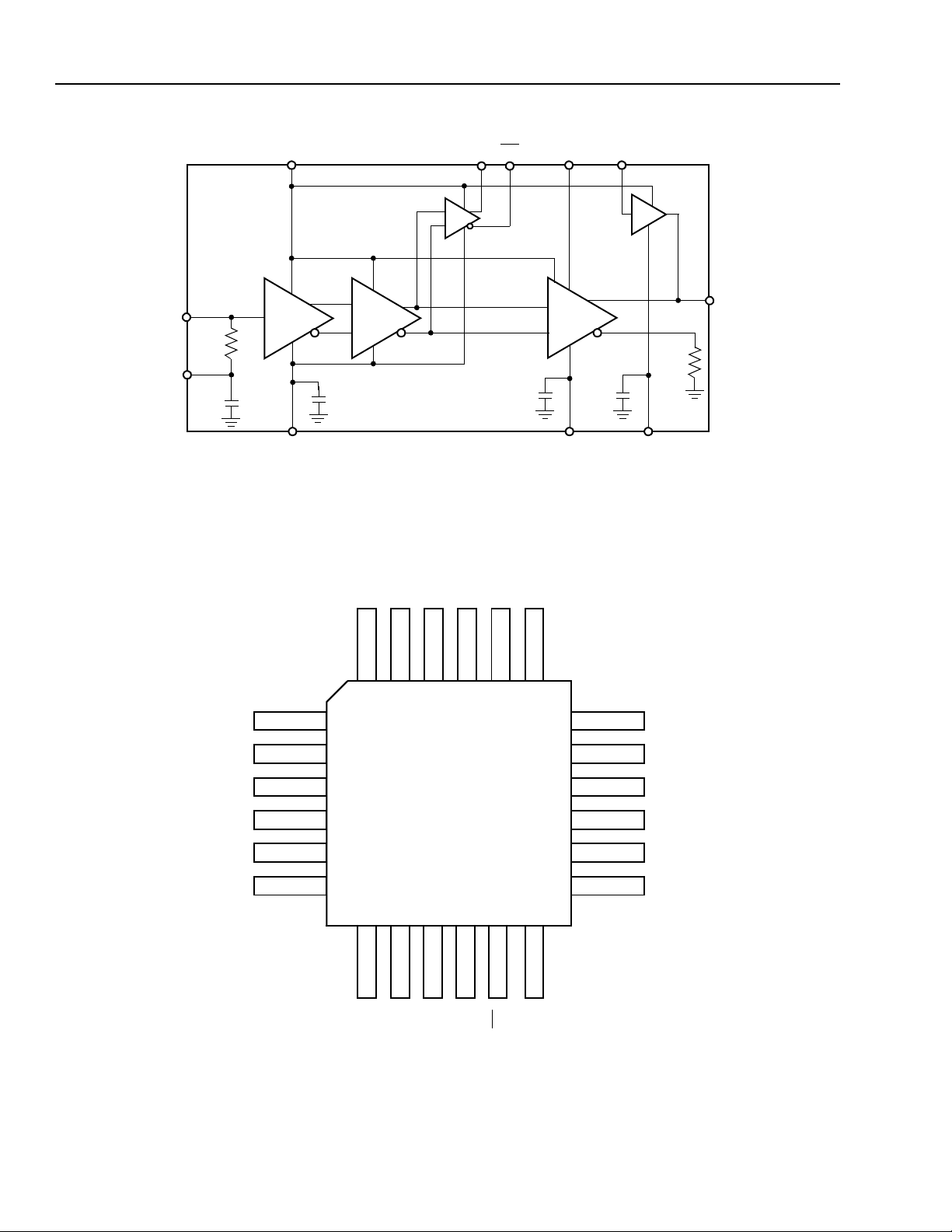
Figure 2. LG1625AXF Die Block Diagram
SS2
SS3
MOD
SS1
SS1
TH
V
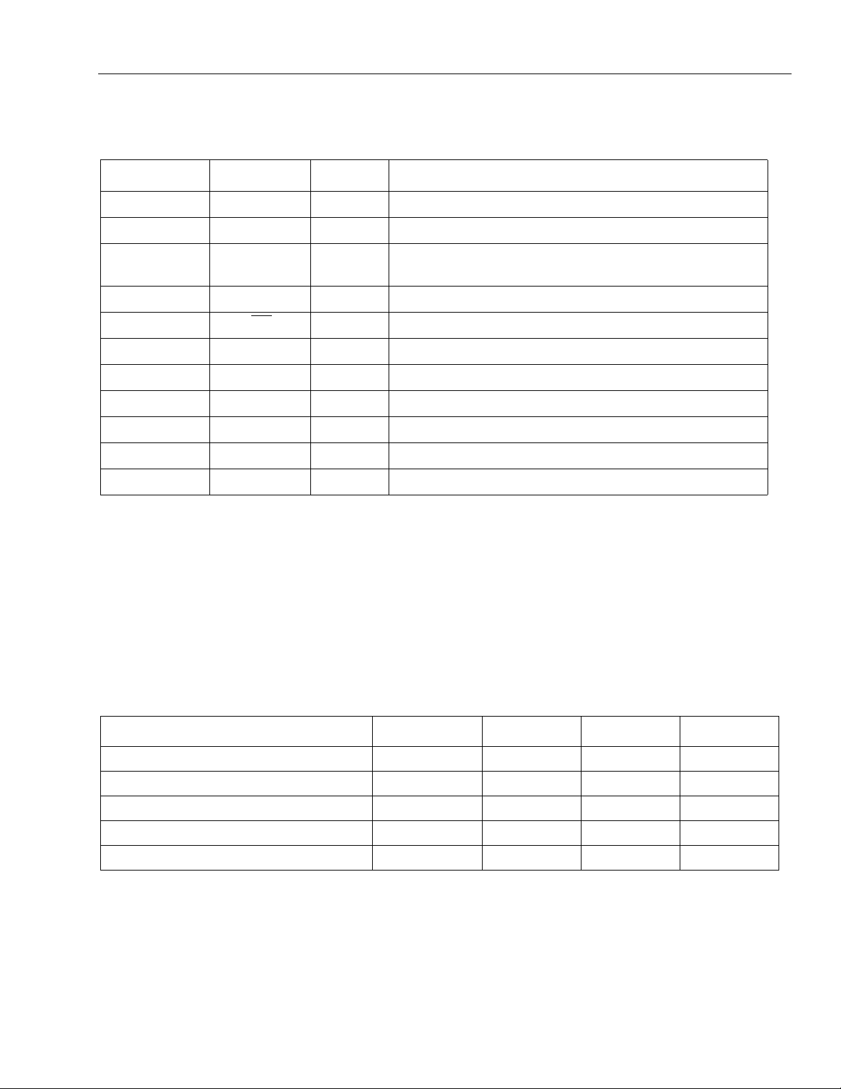
24
V
23
V
22
V
21
1
IN
2
3
LG1625AXF
4
5
613
V
20
V
19
18
17
16
15
14
PRE
V
GND
OUT
I
GND
GND
SS1
V
7
8
9
10
11
12
TH
V
GND
GND
GND
MK
MK
(OPTIONAL)
5-7867(F)r.1
Note: Figure 3 is not to scale.
Figure 3. LG1625AXF Package Pinout
2 Lucent Technologies Inc.
Data Sheet
June 1999
LG1625AXF Laser Driver
Pin Information
(continued)
Table 1. LG1625AXF Pin Description
Pin Symbol Type
1, 6, 13, 22, 23 V
2V
3, 4, 5, 8, 9, 10,
SS1
IN
GND P
14, 15, 17
7, 24 V
TH
†
11 MK
12 MK O
16 I
18 V
19 V
20 V
21 V
* I = input, O = output, P = power.
† Connection to V
Figure 5 on page 6, Typical Test Circuit).
TH
for threshold adjustment should be made through pin 24. Pin 7 is made available f or additional by passing of VTH (See
OUT
PRE
SS2
SS3
MOD
*
Supply.
P
I
V
SS1
Data Input.
–5.2 V power supply pin.
Name/Definition
Ground.
I
O
Threshold Control.
Input (eye crossing).
Complementary Mark Density Output.
Mark Density Output.
O
I
P
P
I
Output.
dc couple to laser cathode.
Prebias Control Input.
.
V
–5.2 V supply for output prebias.
SS2
.
V
–5.2 V supply for output modulation.
SS3
Modulation Current Control Input.
Absolute Maximum Ratings
Stresses in excess of the absolute maximum ratings can cause permanent or latent damage to the device. These
are absolute stress ratings only. Functional operation of the device is not implied at these or any other conditions in
excess of those given in the operational sections of this device specification. Exposure to absolute maximum ratings for extended periods can adversely affect device reliability.
Table 2. Absolute Maximum Ratings
Parameter Symbol Min Max Unit
Supply Voltage V
Storage Temperature T
Operating Case Temperature Range T
Input Voltage V
Power Dissipation P
= 25 °C unless otherwise specified)
(at T
A
SS
stg
C
I
D
—–5.95V
–40 125
°
C
075°C
GND V
SS
V
—1W
Lucent Technologies Inc. 3
Data Sheet
LG1625AXF Laser Driver
June 1999
Handling Precautions
Although protection circuitry has been designed into this device, proper precautions should be taken to avoid exposure to electrostatic discharge (ESD) during handling and mounting. Lucent employs a human-body model (HBM)
and charged-device model (CDM) for ESD-susceptibility testing and protection design evaluation. ESD voltage
thresholds are dependent on the circuit parameters used in the defined model. No industry-wide standard has
been adopted for the CDM. However, a standard HBM (resistance = 1500 Ω, capacitance = 10 0 pF) is w i de ly us ed
and, therefore, can be used for comparison purposes. The HBM ESD threshold presented here was obtained by
using these circuit parameters.
Table 3. ESD Threshold Voltage
Human-Body Model ESD Threshold
Device Voltage
LG1625AXF ≥200 V
Mounting and Connections
Certain precautions must be taken when using solder. For installation using a constant temperature solder, temperatures of under 300 °C may be employed for periods of time up to 5 seconds, maximum. For installation with a soldering iron (battery operated or nonswitching only), the soldering tip temperature should not be greater than 300 °C
and the soldering time for each lead must not exceed 5 seconds.
4 Lucent Technologies Inc.
 Loading...