

AGERE LG1605DXB-TR16, LG1605DXB-FLP Datasheet
Data Sheet
February 1999
Features
■
28 dB gain, 34 dB differential
■
Large dynamic range: >60 dB
■
Wideband response: 8 kHz to 3 GHz
■
Extremely low ±4 ps delay skew across input range
■
Complementary 50 Ω I/Os
■
Surface-mount package
■
Standard ECL supply (400 mW)
Applications
■
Data/clock main amplifier SONET/SDH OC-48/
STM-16 transmission systems, DWDM systems
LG1605DXB Limiting Amplifier
■
Digital video transmission
■
Interface between 1319 receiver and LG1600
clock and data regenerator
■
High-speed comparator
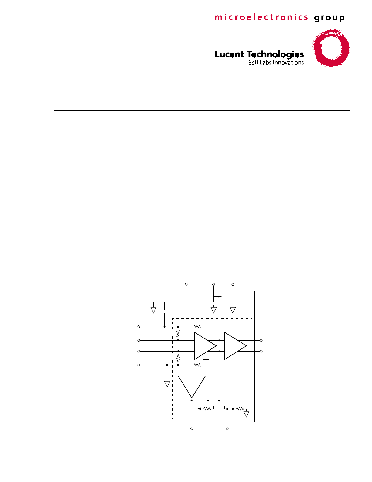
Functional Description
The LG1605DXB is a GaAs wideband limiting amplifier with differential inputs and outputs that provides
28 dB of gain (34 dB differential) and 3 GHz of bandwidth in a 50 Ω environment (Figure 1 shows the
block diagram). At low input levels, below 10 mV to
20 mV, the circuit behaves as a linear amplifier. At
higher levels, the device goes smoothly into limiting.
The device matches the performance of an AGC
amplifier but shows none of the AGC bouncing and
attack characteristics.
V
V
–REF
–IN
V
+IN
V
+REF
10
11
12
9
110 pF
110 pF
50
50
BR
V
8
110 pF
25 k
Ω
Ω
25 k
–+
13 14
BF
V
SS
V
Ω
CHIP BOUNDARY
+––
+
Ω
V
GND
+––
BS
Figure 1. LG1605DXB Block Diagram
1, 4, 5, 6, 15, 167
3
–OUT
V
2
+
V
+OUT
12-3214(F).r3
Data Sheet
LG1605DXB Limiting Amplifier February 1999
Functional Description
(continued)
The amplifier has a virtually constant output delay for
input signal levels, varying across three decades. As a
result, the device has very low amplitude-to-phase conversion, which makes it ultimately suitable for applications in highly sensitive fiber-optic systems. Although
the amplifier is most sensitive when the input is ac coupled (see Figure 3), a low offset (<25 mV) and a large
common-mode input range of 2 V make it useful in
applications that require a high-speed comparator as
well.
A unique input coupling arrangement allows for a frequency response down into the low kHz range while
using coupling capacitors that are small enough to
maintain a good input return loss at high frequencies.
The outputs, when ac coupled, provide a good RF termination up to very high frequencies. The associated
Pin Information
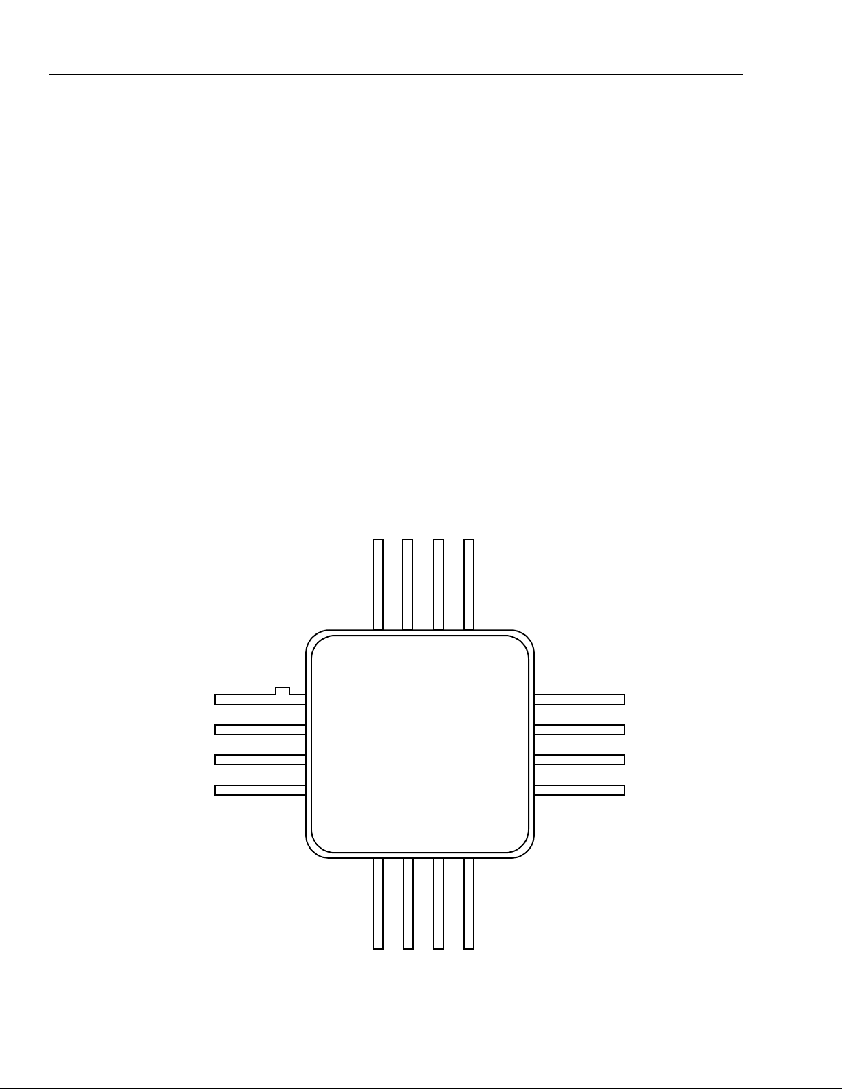
The pinout for the LG1605DXB is shown in Figure 2.
ability to absorb reflections returning from the receiving
end is essential for preventing intersymbol interference
in fiber-optic systems.
The amplifier is a natural step-up interface between
receivers, such as the Lucent Technologies Microeletronics Group Optoelectronics unit 1319 and regenerators like the Lucent Technologies Microelectronics
Group LG1600. The referred wideband input noise
(168 µVrms typical) allows for a <1e–9 bit error rate
(BER) for inputs down to 2 mVp-p (S/N ratio of
21.5 dB).
In SAW based clock recovery systems, with clock fre-
quencies as high as 2.5 GHz, the device can provide a
clock-limiting function in systems.
The LG1605DXB is available in a hermetically sealed,
16-lead, glass-metal surface-mount package and uses
a standard ECL supply.
GND
+OUT
V
–OUT
V
GND
BS
BF
GND GND V
16 15 14 13
1
2
3
4
5678
V
12
11
10
9
V
V
V
V
+REF
+IN
–IN
–REF
GND GND
VSSV
BR
12-3223(F)
Figure 2. Pin Diagram
2 Lucent Technologies Inc.
Data Sheet
February 1999 LG1605DXB Limiting Amplifier
Pin Information
(continued)
The pin descriptions for the LG1605DXB are given in Table 1.
Table 1. Pin Descriptions
Pin Symbol Name/Description
2V
3V
7V
8V
+OUT
–OUT
SS
BR
Positive Data Output.
Negative Data Output.
dc Supply Voltage.
Bias Reference Voltage.
Connect to nominal –1.5 V stable voltage refer-
ence, bypassed to GND with a capacitor ≥0.047 µF.
9V
–REF
Data Negative Reference.
Internally bypassed with 110 pF. Broadband
operation requires up-close external bypassing with a capacitor ≥0.047 µF,
matching the input coupling capacitor.
10 V
–IN
Negative Data Input.
Requires ac-coupling capacitor and 50 Ω source or
termination.
11 V
12 V
13 V
14 V
+IN
+REF
BF
BS
Positive Data Input.
Data Positive Ref erence.
Bias Force Voltage.
Bias Sense Voltage.
Obsolete function, do not connect.
Internal test point, tracking V
See pin 9 above.
nected.
1, 4, 5, 6,
15, 16,
GND
Ground.
For optimum performance, package back should contact board
ground plane. (See the Mounting and Connections section.)
Package
Back
. Normally not con-
BR
3Lucent Technologies Inc.
Data Sheet
LG1605DXB Limiting Amplifier February 1999
Absolute Maximum Ratings
Stresses in excess of the absolute maximum ratings can cause permanent or latent damage to the device. These
are absolute stress ratings only . Functional operation of the device is not implied at these or any other conditions in
excess of those given in the operational sections of the data sheet. Exposure to absolute maximum ratings for
extended periods can adversely affect device reliability.
Table 2. Absolute Maximum Ratings
Parameter Min Max Unit
Supply Voltage Range (V
)–70.5V
SS
P ower Dissipation — 1 W
Voltage (all pins) V
– V
V
V
+REF
–REF
– V
+IN
–IN
SS
—±2V
—±2V
0.5 V
Storage Temperature Range –40 125 °C
Operating Case Temperature Range 0 100 °C
Recommended Operating Conditions
Table 3. Recommended Operating Conditions
Parameter Symbol Min Max Unit
Case Temperature t
Power Supply V
CASE
SS
070°C
–5.7 –4.7 V
Handling Precautions
Although protection circuitry has been designed into this device, proper precautions should be taken to avoid exposure to electrostatic discharge (ESD) during handling and mounting. Lucent employs a human-body model (HBM)
and a charged-device model (CDM) for ESD-susceptibility testing and protection design evaluation. No industrywide standard has been adopted for the CDM. However, a standard HBM (resistance = 1500 Ω
100 pF) is widely used and, therefore, can be used for comparison purposes. The HBM ESD threshold presented
here was obtained by using these circuit parameters.
, capacitance =
Table 4. ESD Threshold
HBM ESD Threshold
Device Voltage
LG1605DXB ≥200 V
Mounting and Connections
Certain precautions must be taken when using solder. For installation using a constant temperature solder, temperatures of under 300 °C may be employed for periods of time up to 5 s, maximum. For installation with a soldering
iron (battery operated or nonswitching only), the soldering tip temperature should not be greater than 300 °C and
the soldering time for each lead must not exceed 5 s. This device is supplied with solder on the back of the package. Due to the high gain of the device, it is recommended to solder the back of the package to ground.
4 Lucent Technologies Inc.
 Loading...