

AGERE LG1602BXB, LG1602AXB Datasheet
Data Sheet
V
+REF
V
+IN
V
–IN
V
–REF
25 k
Ω
110 pF
25 k
Ω
110 pF
D
D
Q
V
+OUTV–OUT
V
SS
V
–CLK
V
+CLK
GND
50
Ω
50
Ω
2 pF
2 pF
50
Ω
50
Ω
February 1999
LG1602 Decision Circuit
Features
■
Operation up to 3 Gbits/s
■
Good sensitivity to low input signals
■
Low power dissipation
■
Surface-mount package
Applications
■
SONET/SDH transmission systems
■
Digital video transmission
■
Digital test instruments
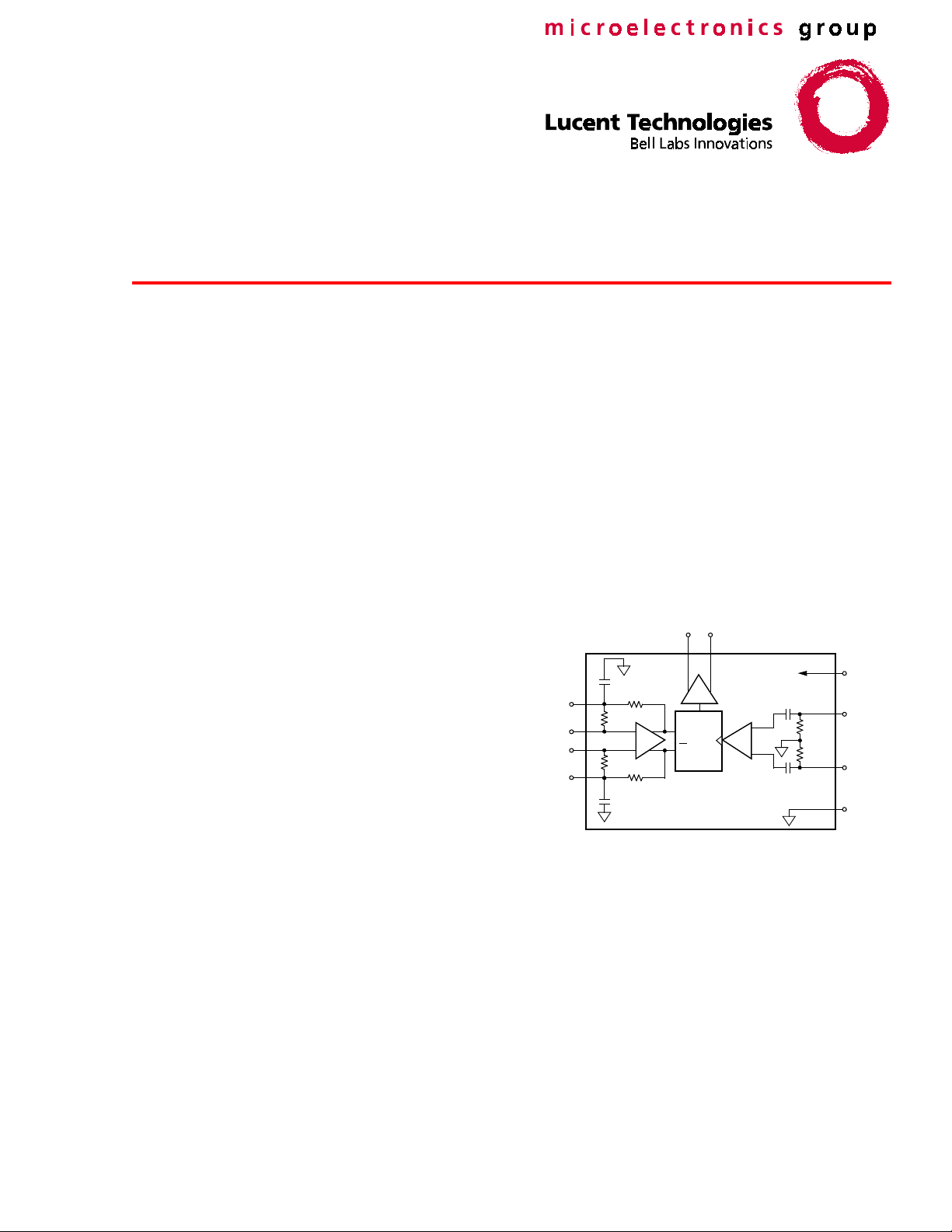
Functional Description
The LG1602 is a gallium arsenide (GaAs) decision
circuit. It features a sensitive broadband input amplifier and a D-type flip-flop that retimes and regenerates an input data stream that is weakened by noise,
jitter, and intersymbol interference.
The LG1602 has complementary 50 Ω output buffers.
dc feedback ensures input threshold control for input
levels as low as 25 mV, when using dc balanced
input data. The LG1602 is available in a hermetically
sealed 16-lead glass-metal surface-mount package.
5-7667(F)r.3
Figure 1. LG1602 Functional Diagram
Data Sheet
y
y
y
µ
µ
y
g
g
LG1602 Decision Circuit February 1999
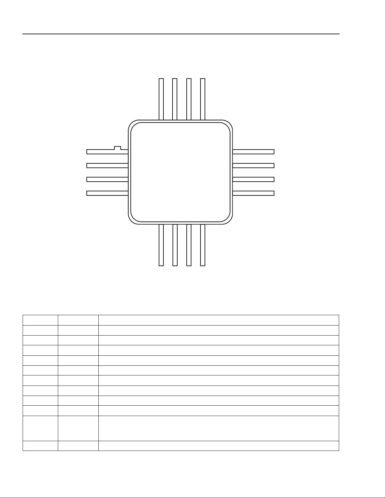
Pin Information
GND
+CLK
V
–CLK
V
GND GND NC
16 15 14 13
1
2
3
SS
V
4
5678
NC
12
11
10
9
V
V
V
V
+REF
+IN
–IN
–REF
–OUTV+OUT
V
NC NC
Figure 2. Pin Diagram
Table 1. Pin Descriptions
Pin Symbol Name/Description
2V
3V
4V
5V
6V
9V
10 V
11 V
12 V
1, 15, 16,
Packa
e
+CLK
–CLK
SS
–OUT
+OUT
–REF
–IN
+IN
+REF
GND
Clock Input.
Clock Input.
Ma
be grounded, if not used.
Ma
be grounded, if not used.
dc Supply Voltage.
Negative Data Output.
Positive Data Output.
ac couple or terminate with 50 Ω to GND.
ac couple or terminate with 50 Ω to GND.
Data Negative Reference.
Negative Data Input.
Positive Data Input.
ac couple with 0.047
ac couple with 0.047
Data Positive Reference.
Ground.
For optimum performance, packa
plane.
B
pass to GND with 0.047 µF in series with 5 Ω.
B
pass to GND with 0.047 µF in series with 5 Ω.
Back
7, 8, 13, 14 NC
No Connection.
12-3223(F).ar.2
F.
F.
e back should contact board ground
2 Lucent Technologies Inc.

Data Sheet
g
g
y
y
g
g
)
February 1999 LG1602 Decision Circuit
Absolute Maximum Ratings
Stresses in excess of the absolute maximum ratings can cause permanent or latent damage to the device. These
are absolute stress ratin
excess of those
iven in the operational sections of the data sheet. Exposure to absolute maximum ratings for
extended periods can adversel
Table 2. Absolute Maximum Ratings
Supply Voltage Range (V
Power Dissipation — 1 W
Voltage (all pins) 0.5 V
Clock Input (V
– V
V
+REF
V
– V
–REF
+CLK
+IN
–IN
Storage Temperature Range –40 125 °C
Operating Case Temperature Range 0 100 °C
s only. Functional operation of the device is not implied at these or any other conditions in
affect device reliability.
Parameter Min Max Unit
)0.5–7V
SS
V
, V
–CLK
SS
—±2V
—±2V
—±2V
Recommended Operating Conditions
Table 3. Recommended Operating Conditions
Parameter Symbol Min Max Unit
Case Temperature t
Power Supply V
CASE
SS
075°C
–4.7 –5.7 V
Handling Precautions
Although protection circuitry has been designed into this device, proper precautions should be taken to avoid e xposure to electrostatic discharge (ESD) during handling and mounting. Lucent employs a human-body model (HBM)
and a charged-device model (CDM) for ESD-susceptibility testing and protection design evaluation. No industrywide standard has been adopted for the CDM. However, a standard HBM (resistance = 1500 Ω, capacitance =
100 pF) is widely used and, therefore, can be used for comparison purposes. The HBM ESD threshold presented
here was obtained by using these circuit parameters.
Table 4. ESD Threshold
HBM ESD Threshold
Device Voltage
LG1602 ≥200 V
Mounting and Connections
Certain precautions must be taken when using solder. For installation using a constant temperature solder, temperatures of under 300 °C ma
solderin
iron (battery operated or nonswitching only), the soldering tip temperature should not be greater than
300 °C and the solderin
be employed for periods of time up to 5 seconds, maximum. For installation with a
time for each lead must not exceed 5 seconds.
3Lucent Technologies Inc.
 Loading...