

AGERE LG1600KXH0622, LG1600KXH2666, LG1600KXH2488, LG1600KXH2380, LG1600KXH1298 Datasheet
...
Data Sheet
June 1999
LG1600KXH Clock and Data Regenerator
Features
■
Integrated clock recovery and data retiming
■
Surface-mount package
■
Single ECL supply
■
Robust FPLL design
■
Operation up to BER = 1e
–3
Figure 1. LG1600KXH Open View
■
SONET/SDH compatible loss of signal alarm
■
High effective Q allows long run lengths
■
Jitter tolerance exceeding ITU-T/Bellcore
■
Low clock jitter generation: <0.005 UI
■
Standard and custom data rates
0.50 Gbits/s—5.5 Gbits/s
■
Complementary 50 Ω I/Os
Applications
■
SONET/SDH receiver terminals and regenerators
OC-12 through OC-96/STM-4 through STM-32
■
SONET/SDH test equipment
■
Proprietary bit rate systems
■
Digital video transmission
■
Clock doublers and quadruplers
Data Sheet
LG1600KXH Clock and Data Regenerator June 1999
Functional Description
The LG1600KXH Clock and Data Regenerator (CDR)
is a compact, single device solution to clock recovery
and data retiming in high-speed communication systems such as fiber-optic data links and long-span fiberoptic regenerators and terminals. Using frequency and
phase-lock loop (FPLL) techniques, the device regenerates clean clock and error-free data signals from a
nonreturn-to-zero (NRZ) data input, corrupted by jitter
and intersymbol interference. The LG1600KXH
exceeds ITU-T/Bellcore jitter tolerance requirements
for SONET/SDH systems.
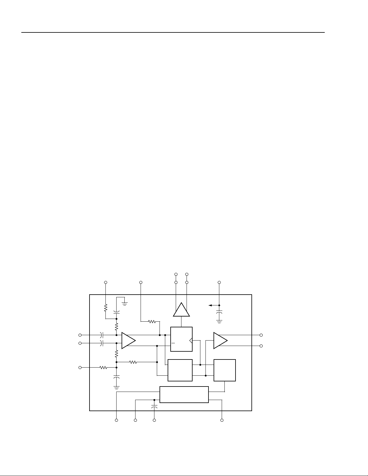
The device houses two integrated circuits on an alumina substrate inside a hermetically sealed 3 cm ×
3cm (1.2in. × 1.2 in.) surface-mount package: a GaAs
IC that contains the high-speed part of an FPLL as well
as a highly sensitive decision circuit; and a silicon bipolar IC that contains a loop filter, acquisition, and signal
detect circuitry.
The two ac-coupled complementary data inputs can be
driven differentially as well as single ended. A dc feedback voltage V
V
(decision level) that is optimum for a wide range
–TH
of 50% duty cycle input levels (connect to V
needed, the user can supply an external threshold to
compensate for different mark densities or distorted
input signals (see Figure 10).
maintains a data input threshold
–FB
–TH
). If
Regenerated clock and data are available from complementary outputs that can either be ac coupled, to provide 50 Ω output match, or dc coupled with 50 Ω to
ground at the receiving end.
The second-order PLL filter bandwidth is set by the
user with an external resistor between pin 11 and
ground (required). An internal capacitor provides sufficient PLL damping for most applications. In critical
applications, PLL damping can be increased using an
external capacitor between pins 9 and 11.
The device is powered by a single –5.2 V ECL compatible supply and typically consumes 1.5 W.
The LG1600KXH comes in standard bit rates, but can
be factory tuned for any rate between 500 Mbits/s and
5500 Mbits/s.
A test fixture (TF1004A) with SMA connectors is available to allow quick evaluation of the LG1600KXH.
Theory of Operation
A digital regenerator has the task of retransmitting a bit
stream that is received from a remote source with the
same fidelity at which it was originally transmitted.
Two basic properties of the digital signal need to be
restored: the timing of the transitions between the bits
and the value of each bit.
SS
–TH
V
51
Ω
1 k
0.047 µF
55
–IN
V
60
+IN
V
0.047 µF
1 k
65
+FB
V
0.047 µF
50
50
Ω
0.047 µF
REF
V
V
48
Ω
Ω
Ω
25 k
EXTREXT
C
–FB
+OUT
V
Ω
25 k
LOOP CONTROL &
SIGNAL DETECT
0.047 µF
1197
43 38
Q
D
D
FREQ. &
PHASE
DETECT.
V
–OUT
0
90
V
35
0.047 µF
31
+CLKO
V
26
–CLKO
V
°
°
VCO
LOS
12-3225(F)r.5
Figure 2. LG1600KXH Block Diagram
2 Lucent Technologies Inc.
Data Sheet
PDQ
PDI
LOGIC
TO FLIP-FLOP
FROM
VCO
90
°
0
°
TRANSITION
PULSE
DATA
CIRCULATOR
DELAYED
DATA
STUB
FPD OUT
90
°
0
°
TRANSITION
DELAYED
DATA
1/2 T
1/4 T
DATA
PULSE
CLOCK
CLOCK
T
June 1999 LG1600KXH Clock and Data Regenerator
Theory of Operation
(continued)
Consequently, the timing information that is present in
the data needs to be extracted and a decision as to the
value of each bit must be made. Both timing instant and
decision levels are critical, since the economics of data
transmission dictate the largest distance possible
between transmitter and receiver. A practically closed
data eye can therefore be expected at the output of the
receiver, allowing only a small decision window.
An added complication in nonreturn-to-zero (NRZ) systems is the absence of clock component in the data
signal itself. Practical clock recovery circuits have used
a combination of nonlinear processing to extract a
spectral component at the clock frequency and narrowband filtering using a SAW filter or dielectric resonator.
The relative bandwidth of such a filter must be on the
order of a few tenths of a percent to minimize the data
pattern dependence of the resulting clock. T emperature
behavior of the passband characteristics, such as
group delay, must be tightly matched to that of the data
path. These extreme requirements make such a discrete design very difficult to manufacture at Gbits/s
data rates.
The LG1600KXH clock and data regenerator relies on
phase-lock loop techniques, rather than passive filtering. The filter properties of a PLL are determined at low
frequencies where parasitic elements play only a minor
roll and stability is easily maintained. Furthermore, the
reference frequency is determined by the data rate
itself, rather than by the physical properties of a bandpass filter.
12-3226(F)r.3
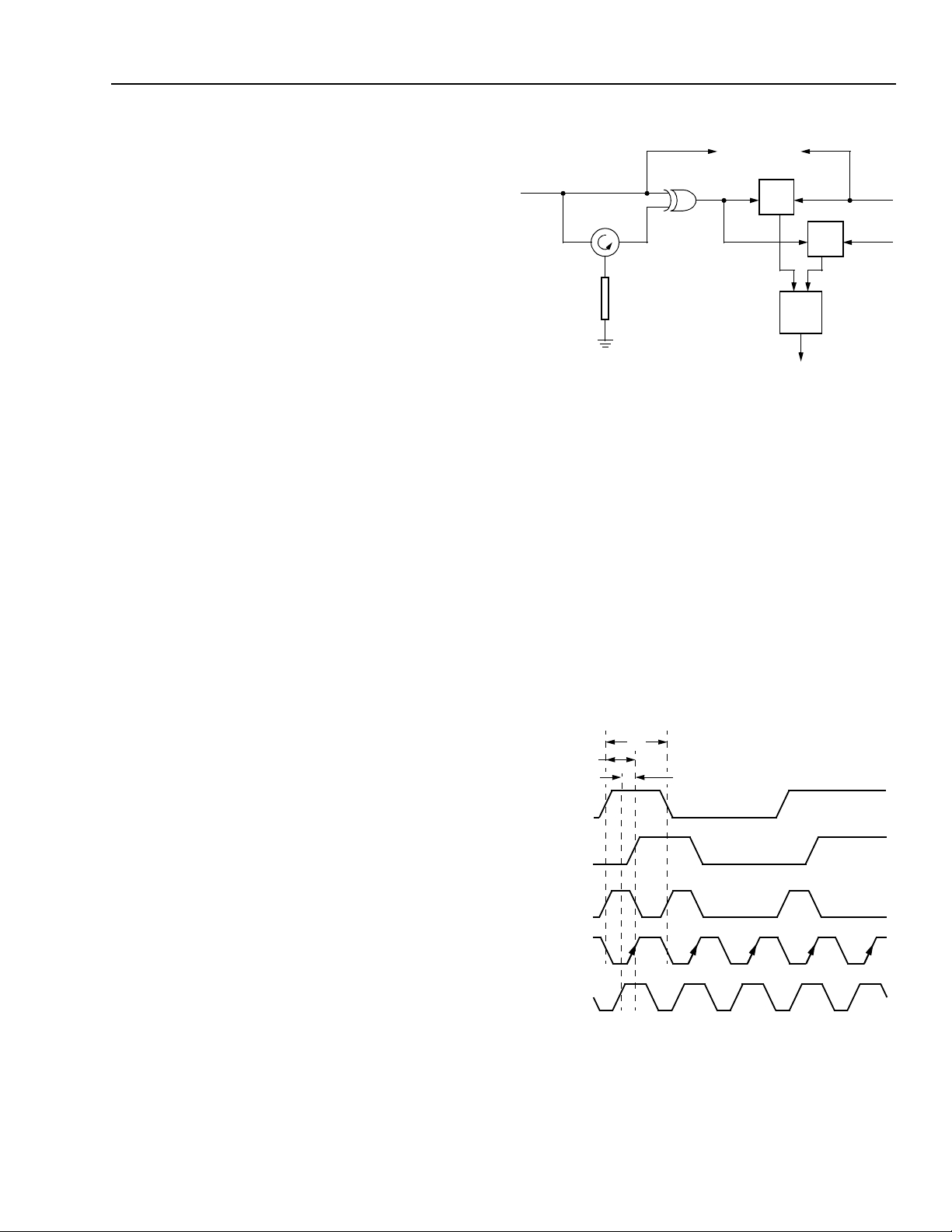
Figure 3. Frequency and Phase Detector
For a transition pulse of half the width of the bit period,
the timing diagram of Figure 4 shows how the in-phase
clock ends up in the center of the data eye when the
quadrature-phase detector output is forced to zero by
the loop. The (patented) transition detector is comprised of an (active) circulator, a shorted stub, and an
exclusive-OR gate. The circulator/stub combination
produces a delayed version of the data. A transition at
the input of the circuit results in an output pulse from
the exclusive-OR gate whose width equals the return
delay of the stub. The stub is tuned for a given bit rate
and can be adjusted so that the in-phase clock is
exactly centered in the error-free phase range of the
retiming flip-flop.
Although PLLs can eliminate some of the shortcomings
of passive bandpass filters used in clock recovery circuits, care was taken in the design of the LG1600KXH
to preserve desired properties such as linearity of the
jitter characteristics. A linear jitter transfer makes it a lot
easier for the system designer to predict the overall
performance of a link.
As a result, the architecture chosen for the device is not
basically different from the conventional clock recovery
circuit. A transition detector extracts a pulse train from
the incoming data signal which is used as a reference
signal for a PLL. The transition pulse train can be seen
as a clock signal that is modulated with the instantaneous transition density of the data signal. The PLL
locks onto the frequency and phase of this pulse train
and freewheels during times when transitions are
absent. The LG1600KXH features dual phase detectors; one driven by an in-phase clock which is also driving the decision circuit flip-flop, the other is driven by a
quadrature clock. The phase detectors produce a zero
output when their respective clocks are centered with
respect to the transition pulses.
12-3227(F)r.2
Figure 4. Timing Diagram
3Lucent Technologies Inc.
Data Sheet
LG1600KXH Clock and Data Regenerator June 1999
Theory of Operation
–360
°
–180
°
(continued)
FPD OUT
0
°
180
°
360
°
PHASE
12-3228(C)r.4
Figure 5. Frequency and Phase Detector
Characteristics
The frequency detector is not a separate function but
an integral part of the phase-lock loop. Any transition
between frequency and phase acquisition is completely
avoided. Figure 5 shows the output characteristics of
the FPD, which is essentially an extended range phase
detector. The two quadrature clock phases are used to
produce hysteresis, which extends the phase detector
range to ±270°. The extended range gives the phase
detector a static frequency sensitivity as demonstrated
in Figure 6. For clock frequencies lower than the bit rate
(the phase is increasing), the top trajectory of the diagram in Figure 6 is followed. When the VCO frequency
exceeds the bit rate, the lower trajectory applies. Since
the linear part of the phase detector produces a netzero output, in the first instance, positive pulses are fed
into the loop filter increasing the VCO frequency, while
in the latter case, the FPD produces negative pulses.
The wide, 540° range of the phase detector is also
responsible for the high jitter tolerance of the
LG1600KXH and an associated immunity to cycle slip
under high jitter conditions. The clock can be momentarily misaligned as much as 270° but still return to its
original position. This property is extremely important
in synchronous systems, since a cycle slip would cause
misalignment of the demultiplexer following the circuit
resulting in a loss of frame condition. The LG1600KXH
can handle bit error rates up to 1e
–3
as a result of low-
frequency jitter.
FPD
OUT
TIME
B
TIME
B
12-3229(C)r.3
FPD
OUT
A. fck < f
B. fck > f
Figure 6. Frequency Detector Operation
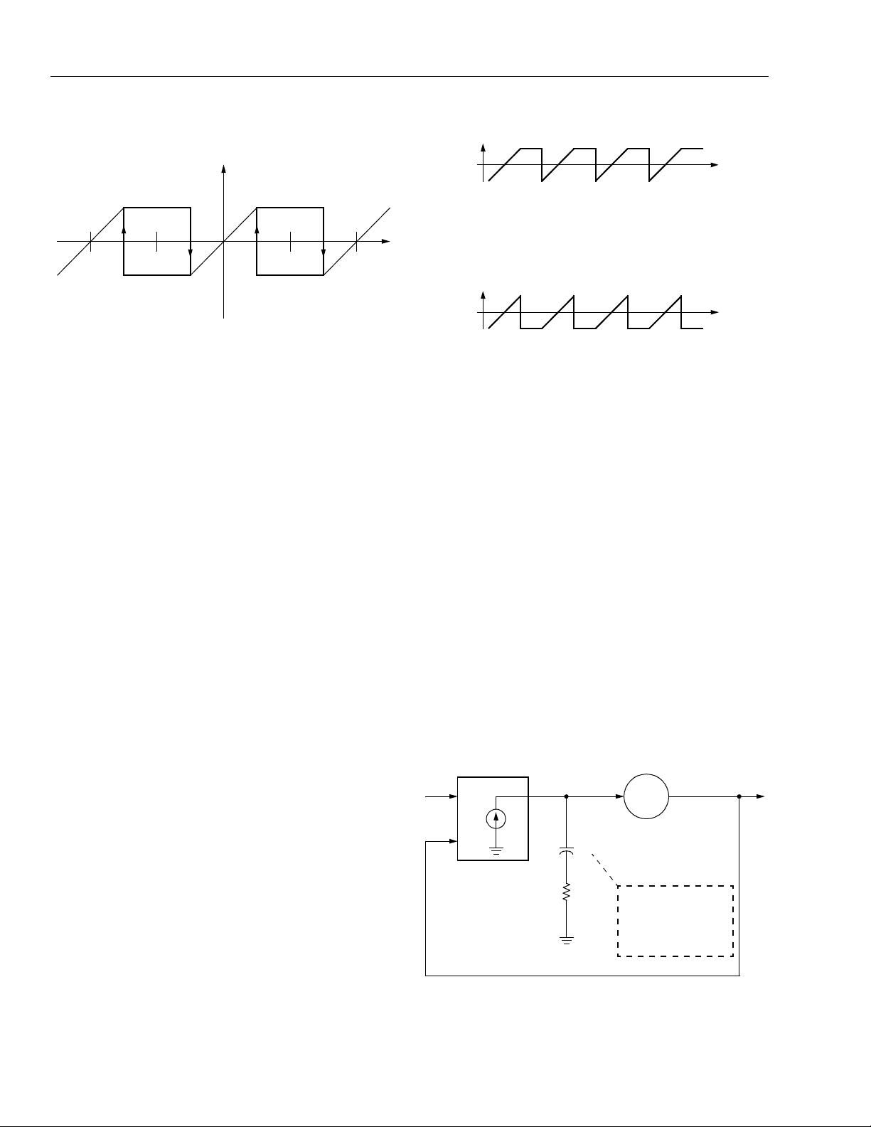
PLL Dimensioning
The LG1600KXH CDR employs a heavily damped
second-order phase-lock loop. A linear model of this
PLL is depicted in Figure 7. The conventional secondorder equation describing the jitter transfer of the PLL
is shown below:
ϕ
where ϕ
Hs()
and ϕ
i
o
----- -
==
s()
ϕ
i
denote the input and output phase,
o
2ςω
-----------------------------------------
2
s
2ςωns ω
++
respectively, ς is the PLL damping ratio and ω
natural frequency . F or most clock recov ery applications
a very high damping is required that renders the PLL
essentially as a first-order system with a slight peaking
that is generally undesirable. The second-order equation above does not provide much insight into the peaking and bandwidth parameters.
ϕ
i
Kd
C
PHASE DETECTOR
Rx
VCO
SUM OF INTERNAL
AND EXTERNAL
CAPACITANCE
2
n
n
s ω
+
2
n
Ko
LOOP FILTER
is the
n
ϕ
o
12-3230(F)r.4
Figure 7. Phase-Lock Loop Linear Model
4 Lucent Technologies Inc.
Data Sheet
Hs()
max
1
1
ω
b
τ
---------
+≈ 1
1
R
x
2
CKdK
o
------------------------ -
+=
June 1999 LG1600KXH Clock and Data Regenerator
Theory of Operation
(continued)
A more useful expression of the PLL characteristics is
*
the following
:
Hs()
b
1
ω
=
-------------------------------------
b
+
s ω
1
+
----sτ
1
1
-----+
sτ
The jitter transfer is now directly expressed in the physical loop gain pole product, ω
constant, τ. Damping ratio, ς, and natural frequency, ω
, and the loop filter time
b
n
simply relate to these two parameters as follows:
0.5
τ
ςω
=
b
and
n
* Wolaver, D.H.,
1991.
ω
Phase-Locked Loop Circuit Design
ωnτ⁄=
, Prentice Hall,
For moderate damping, ς > 2.5 (ω
τ < 0.1), the –3 dB
b
bandwidth of the PLL can be approximated by the loop
gain pole product:
J
≈ ωb = KdRxK
BW
o
while the jitter peaking can be expressed in terms of
the product of PLL bandwidth and loop filter time constant:
As the last two expressions make clear, the PLL band-
,
width is controlled by the value of the external resistor
(see Figure 8), while the peaking depends both on the
resistor value (quadratically) and total loop filter capacitance.
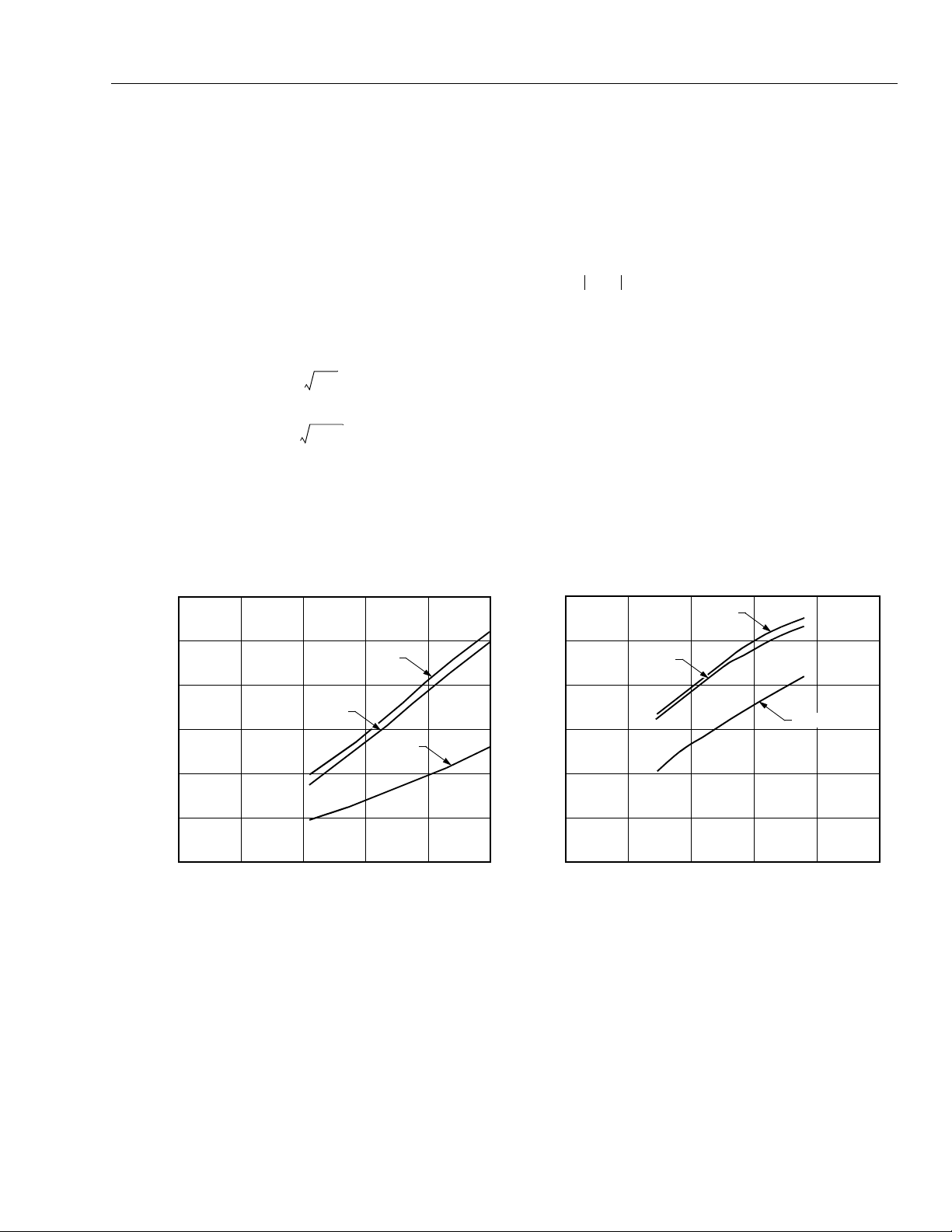
1.2
1.0
C
10
°
0.8
C
25
°
0.6
(MHz)
BW
J
0.4
0.2
0.0
0 50 100 200 250
Rx (
Ω
A. LG1600KXH0622 (Cx = 0.15
70
150
)
Figure 8. Jitter Bandwidth vs. External Resistor Value
3.6
3.0
25 °C
2.4
1.8
(MHz)
C
°
F)
µ
BW
J
1.2
0.6
0.0
0 50 100 200 250
B. LG1600KXH2488 (Cx = 0)
10
Rx (
C
°
70 °C
150
)
Ω
12-3231(F)r.3—12-3232(F)r.3
5Lucent Technologies Inc.
Data Sheet
LG1600KXH Clock and Data Regenerator June 1999
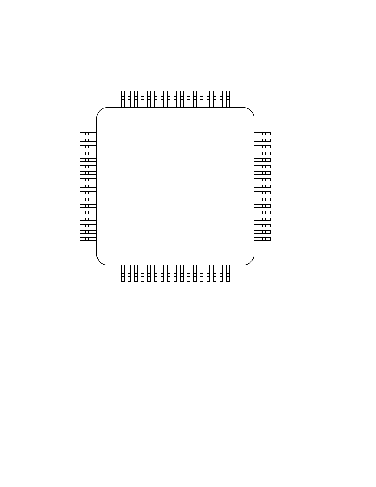
Pin Information
The pinout for the LG1600KXH is shown in Figure 9.
DNC
GND
GND
DNC
GND
GND
REF
V
GND
EXT
C
GND
EXT
R
GND
GND
LOS
GND
GND
DNC
1
2
3
4
5
6
7
8
9
10
11
12
13
14
15
16
17
GND
GND
+FB
V
GND
GND
NIC
68 65
19 20 21 22 23 24 25 27 28 29 30 32 33
18 26 31 34
+IN
V
GND
GND
GND
GND
GND
GND
60 55 52
–IN
V
GND
53545657585967 66 64 63 62 61
GND
GND
51
50
49
48
47
46
45
44
43
42
41
40
39
38
37
36
35
–TH
V
GND
GND
–FB
V
GND
GND
GND
GND
+OUT
V
GND
GND
GND
GND
–OUT
V
GND
GND
SS
V
NIC
GND
GND
GND
GND
GND
GND
GND
GND
GND
GND
GND
GND
–CLKO
V
GND
+CLKO
V
GND
12-3233(F)r.1
Figure 9. Pin Diagram
6 Lucent Technologies Inc.
 Loading...