

AGERE LCK4953 Datasheet
LCK4953
Low-Voltage PLL Clock Driver
Data Sheet
November 2001
Features
• Fully integrated PLL
• Output frequency up to 130 MHz in PLL mode
• Nine outputs with high-impedance disable
• 32-lead TQFP
• 50 ps cycle-to-cycle jitter
• Pin compatible with the Motorola
driver
®
MPC953 clock
Description
The LCK4953 is a PLL-based clock driver device
intended for high-performance clock tree designs.
The LCK4953 is 3.3 V compatible with output
frequencies of up to 130 MHz and output skews of
75 ps. The LCK4953 can meet the most demanding
timing requirements and employs on-chip voltage
regulators to minimize cycle-to-cycle jitter and phase
jitter.
The LCK4953 is ideal for use as a zero delay, low
skew, fan-out buffer due to its differential LVPECL
reference input along with an exter nal feedba ck
input. The MROEB pin of the LCK4953, when driven
high, will reset the internal counters and 3-state the
output buffers. The LCK4953 has been optimized for
zero delay performance.
The LCK4953 is fully 3.3 V compatible and requires
no external loop filter components. All control inputs
accept LVCMOS or LVTTL compatible levels while
the outputs provide LVCMOS levels with the ability to
drive terminated 50 Ω transmission lines. For seriesterminated 50 Ω lines, each of the LCK4953 outputs
can drive two traces giving the device an effective
fan-out of 1:18. For the optimum combination of
board density and performance, the device is
packaged in a 7 mm × 7 mm 32-lead TQFP package.
Table 1. Function Table
BYPASSB Function
1
0
MROEB Function
1
0
VCOSEL Function
1
0
PLLEN Function
1
0
PLL Enabled
PLL Bypass
Outputs Disabled
Outputs Enabled
÷ 8
÷ 4
Select VCO
Select PELCLK
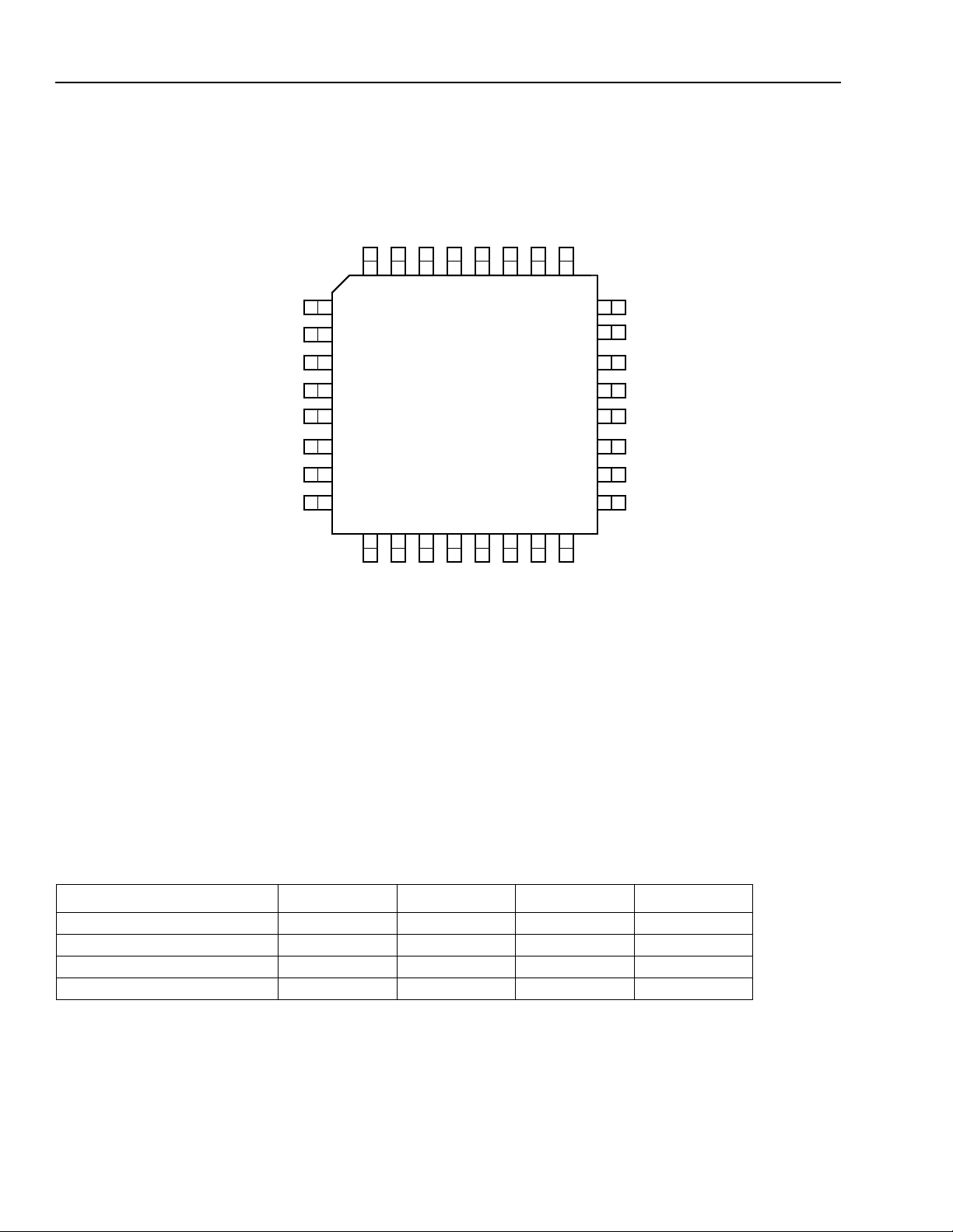
LCK4953
Low-Voltage PLL Clock Driver
Description (continued)
Data Sheet
November 2001
VDDA
FBCLK
NC1
NC2
NC3
NC4
V
SSA
PECLCKP
QFB
28
13
SS
V
DD
V
27
14
Q6
Q0
26
15
DD
V
SS
V
PLLEN
BYPASSB
VCOSEL
29
30
31
32
1
2
3
4
5
6
7
8
9
PECLCKN
10
MROEB
LCK4953
12
11
DD
Q7
V
Figure 1. 32-Lead Pinout (Top View)
SS
V
25
16
Q5
24
23
22
21
20
19
18
17
Q1
V
Q2
V
Q3
V
Q4
V
DD
SS
DD
SS
5-8653(F)
Absolute Maximum Ratings
Stresses which exceed the absolute maximum ratings can cause permanent damage to the device. These are
absolute stress ratings only. Functional operation of the device is not implied at these or any other conditions in
excess of those given in the operational sections of the data sheet. Exposure to absolute maximum ratings for
extended periods of time can adversely affect device reliability.
Table 2. Absolute Maximum Ratings
Parameter Symbol Min Max Unit
Supply Voltage V
Input Voltage V
Input Current I
Storage Temperature Range T
2 Agere Systems Inc.
DD –0.3 4.2 V
IN –0.3 VDD + 0.3 V
IN — ±20 mA
stg –40 125 °C
 Loading...