

AGERE LCK4950 Datasheet

LCK4950
Low-Voltage PLL Clock Driver
Data Sheet
November 2001
Features
■ Fully integrated phase-locked loop (PLL)
■ Oscillator or crystal reference input
■ Output frequency up to 180 MHz
■ Outputs disable in high impe dan ce
■ Compatible with PowerPC
®
, Intel®, and high-
performance RISC microprocessors
■ TQFP packaging
■ Output frequency configurable
■ ±35 ps typical cycle-to-cycle jitter
■ Pin compatible with the Motorola
®
MPC950 clock
driver
Description
The LCK4950 is a PLL-based clock driver device
intended for high-performance clock tree designs.
The LCK4950 is 3.3 V compatible with output
frequencies of up to 180 MHz and output skews of
200 ps. The LCK4950 can accommodate the most
demanding tree designs by employing a fully
differential PLL design. This minimizes cycle-to-cycle
jitter, which is critical when the device is acting as the
reference clock for PLLs in today’s microprocessor s
and ASICs. The device has nine low-skew
configurable outputs for support of the clocking
needs of the various high-performa nce
microprocessors.
To provide input reference clock flexibility, two
selectable division ratios are available on the
LCK4950. The internal V
CO runs at either 2x or 4x
the high-speed output. The FBSEL pin is used to
select between a divide by 8 or a divide by 16 of the
CO frequency to be compared with the input
V
reference. These selections allow the input reference
to be either one-half, one-fourth, or one-eighth of the
high-speed output.
The LCK4950 is capable of scan clock distribution or
system diagnostics due to an external test clock
input. The REF_SEL pin allows the selection
between a crystal input to an on-chip oscillator for the
reference or selection of a TTL level oscillator input
directly. Only a parallel resonant crystal is required
for the onboard crystal oscillator external
components.
The LCK4950 is fully 3.3 V compatible and requires
no external loop filter components. All inputs accept
LVCMOS or LVTTL compatible levels while the
outputs provide LVCMOS levels with the capability to
drive terminated 50 Ω transmission lines. The
LCK4950 can drive two traces, giving the device an
effective fan out of 1:18 for series-terminated 50 Ω
lines. For optimum performance and board density,
the device is packaged in a 7 mm x 7 mm 32-lead
TQFP package.
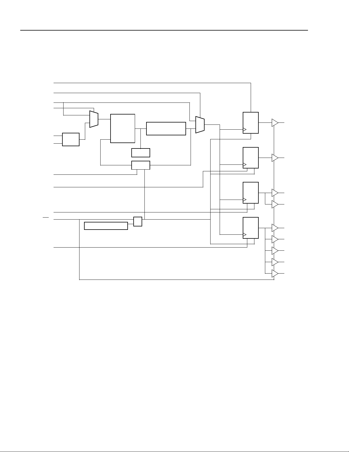
LCK4950
Low-Voltage PLL Clock Driver
Description (continued)
fsela
PLL_En
Tclk
Ref_Sel
Data Sheet
November 2001
xtal1
xtal2
FBsel
fselb
fselc
MR/OE
fseld
xtal
OSC
(PULL-DOWN)
PHASE
DETECTOR
POWER-ON RESET
200 MHz—480 MHz
LPF
÷8/÷16
CO)
(V
÷2/÷4
÷4/÷8
÷4/÷8
÷4/÷8
Qa
Qb
Qc0
Qc1
Qd0
Qd1
Qd2
Qd3
Qd4
5-9698 (F)
Figure 1. Logic Diagram
2 Agere Systems Inc.
Data Sheet
November 2001
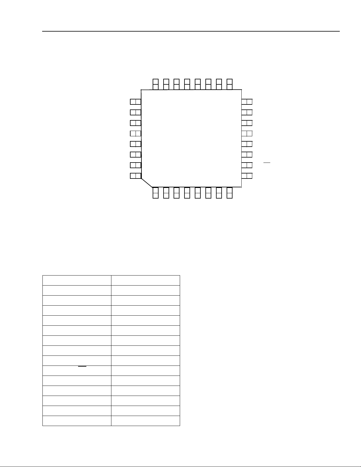
Pin Information
LCK4950
Low-Voltage PLL Clock Driver
VSS
Qb
V
DD
Qa
V
SS
TCLK
PLL_En
Ref_Sel
DD
Qc1
V
Qc0
22
23
24
25
26
27
28
29
30
31
32
1
DDA
V
2
FBsel
LCK4950
3
fsela
Figure 2. Pin Diagram
SS
V
21
4
fselb
Qd0
20
5
fselc
DD
V
19
6
fseld
Qd1
18
7
SS
V
SS
V
17
8
xtal1
16
15
14
13
12
11
10
Qd2
V
DD
Qd3
SS
V
Qd4
V
DD
MR/OE
9
xtal2
5-9699 (F)
Functional Description
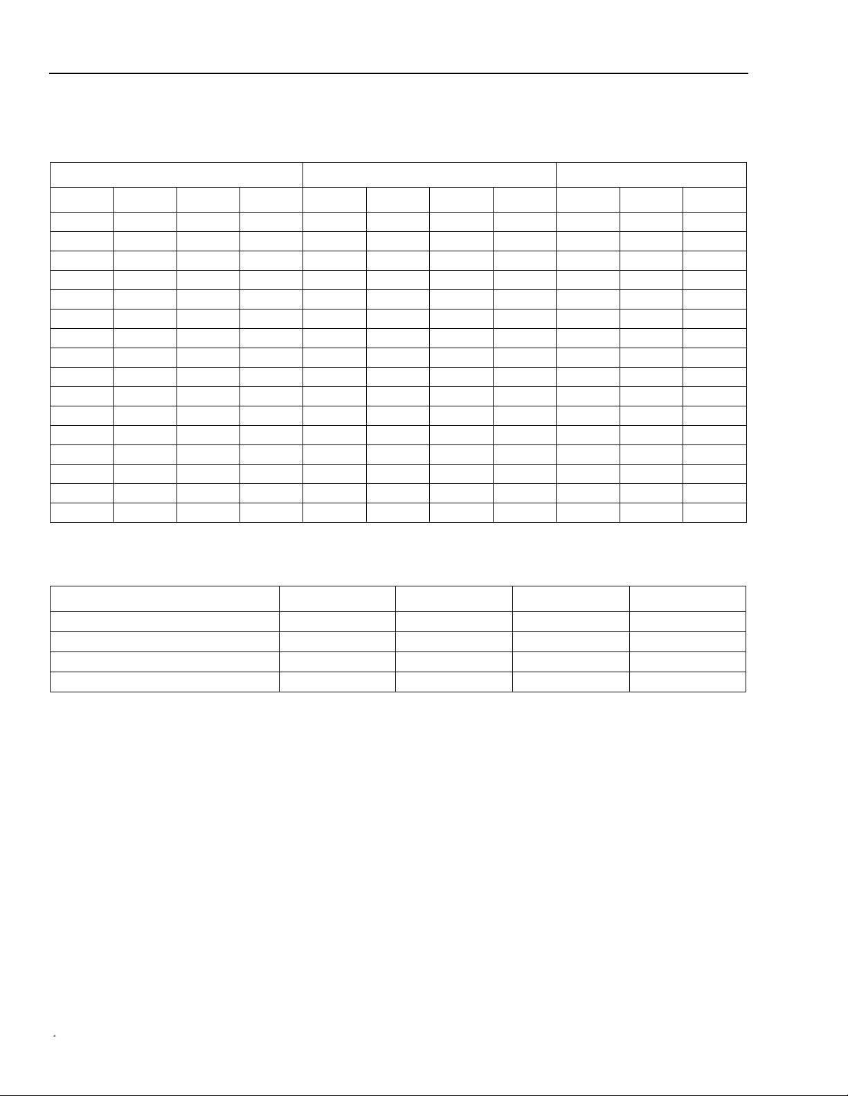
Table 1. Function Tables
Ref_Sel Function
1TCLK
0XTAL_OSC
PLL_En Function
1 PLL Enabled
0 PLL Bypass
FBsel Function
1 ÷8
0 ÷16
MR/OE
1 Outputs Disabled
0 Outputs Enabled
fseln Function
1Qa = ÷4; Qb:d = ÷8
0Qa = ÷2; Qb:d = ÷4
Function
Agere Systems Inc. 3
LCK4950
Low-Voltage PLL Clock Driver
Data Sheet
November 2001
Functional Description (continued)
Table 2. Function Table
Inputs Outputs Totals
fsela fselb fselc fseld Qa(1) Qb(1) Qc(2) Qd(5) T otal 2x T otal x T otal x/2
00002xxxx180
00012xxxx/2135
00102xxx/2x162
00112xxx/2x/2117
01002xx/2xx171
01012xx/2xx/2126
01102xx/2x/2x135
01112xx/2x/2x/2108
1000xxxx090
1001xxxx/2045
1010xxx/2x072
1011xxx/2x/2027
1100xx/2xx081
1101xx/2xx/2036
1110xx/2x/2x063
1111xx/2x/2x/2018
Note: x = fVCO/4; 200 MHz < fVCO < 480 MHz.
Table 3. PLL Input Reference Characteristics
Characteristic Symbol Min Max Unit
TCLK Input Rise/Falls t
Reference Input Frequency f
Crystal Oscillator Frequency
†
Reference Input Duty Cycle f
* Maximum and minimum input reference is limited by the VCO lock range and the feedback divider for the TCLK or xtal1 inputs.
†See the Applications section for more crystal information.
r, tf — 3.0 ns
ref —* —*MHz
fXtal 12.5 25 MHz
refdc 25 75 %
44 Agere Systems Inc.
Data Sheet
November 2001
Low-Voltage PLL Clock Driver
LCK4950
Applications
Programming the LCK4950S
Several frequency relationships are configurable by the LCK4950. Frequency ratios of 1:1, 2:1, 4:1, and 4:2:1 are
possible from configuring the output dividers for the four output groups. To ensure that the output duty cycle is
always 50%, the LCK4950 uses even dividers. Table 4 illustrates output configurations of the LCK4950, describing
the outputs using the V
CO/4, and the Qd to VCO/8 would provide the output frequency relationship of 4:2:1.
to V
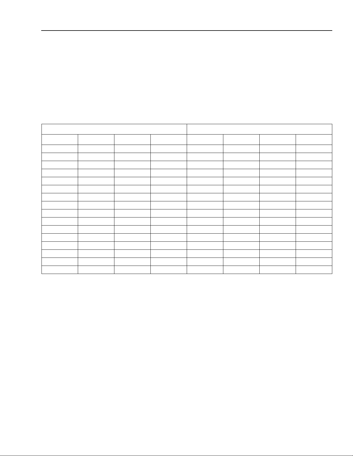
Table 4. Programmable Output Frequency Relationships
FSELA FSELB FSELC FSELD Qa Qb Qc Qd
0000V
0001V
0010V
0011VCO/2 VCO/4 VCO/8 VCO/8
0100V
0101V
0110VCO/2 VCO/8 VCO/8 VCO/4
0111V
1000V
1001VCO/4 VCO/4 VCO/4 VCO/8
1010V
1011V
1100VCO/4 VCO/8 VCO/4 VCO/4
1101V
1110V
1111VCO/4 VCO/8 VCO/8 VCO/8
CO frequency as a reference. For example, setting the Qa outputs to VCO/2, the Qb and Qc
Inputs Outputs
CO/2 VCO/4 VCO/4 VCO/4
CO/2 VCO/4 VCO/4 VCO/8
CO/2 VCO/4 VCO/8 VCO/4
CO/2 VCO/8 VCO/4 VCO/4
CO/2 VCO/8 VCO/4 VCO/8
CO/2 VCO/8 VCO/8 VCO/8
CO/4 VCO/4 VCO/4 VCO/4
CO/4 VCO/4 VCO/8 VCO/4
CO/4 VCO/4 VCO/8 VCO/8
CO/4 VCO/8 VCO/4 VCO/8
CO/4 VCO/8 VCO/8 VCO/4
The division settings establish the output relationship, but one must still ensure that the V
frequency of the outputs desired. The feedback frequency should be used to situate the V
CO will be stable given the
CO into a frequency
range in which the PLL will be stable. The design of the PLL is such that for output frequencies between 25 MHz
and 180 MHz, the LCK4950 can generally be configured into a stable region.
Agere Systems Inc. 5
 Loading...