

AGERE LCK4802 Datasheet
LCK4802
Low-Voltage PECL Differential Clock
Preliminary Data Sheet
July 2001
General
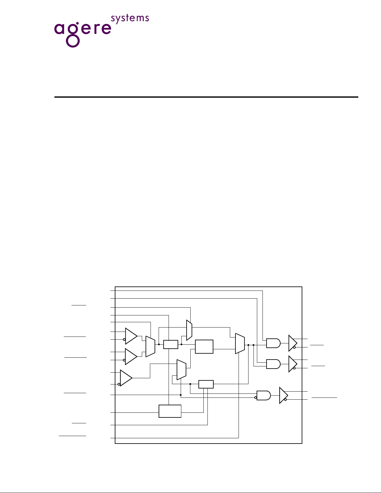
The LCK4802 is a low-voltage, 3.3 V PECL
differential clock synthesizer. The LCK4802 supports
two differential PECL output pairs with frequencies
from 336 MHz to 1 GHz. The clock is designed to
support single and multip le proces so r systems that
require PECL differential inputs. The LCK4802
contains a fully integrated PLL (phase-locked loop)
which multiplies the PECL_CLK input frequency to
match individual processor clock frequencies. The
PLL can be bypassed so that the PCLK outputs are
fed from the PECL_CLK or PECL_CLK input for test
purposes. All outputs are powered from a 2 V
external supply to reduce on-chip power
consumption. All outputs are PECL. The PLL can
operate in the internal feedback mode, or in the
external feedback mode for board level debugging
applications.
Description
Features
■
Two fully selectable clock inputs.
■
Fully integrated PLL.
■
336 MHz to 1 GHz output frequencies.
■
PECL outputs.
■
PECL reference clock.
■
32-pin TQFP package.
PCLK0_EN (PULL-UP)
PCLK1_EN (PULL-UP)
TESTM
(PULL-UP)
PLLREF_EN (PULL-UP)
REF_SEL (PULL-UP)
PECL_CLK (PULL-UP)
PECL_CLK
PECL_CLK (PULL-UP)
PECL_CLK
EXTFB_EN
PLL_BYPASS
(PULL-UP)
(PULL-UP)
(PULL-UP)
EXTFB_IN (PECL)
(PULL-DOWN)
(PULL-UP)
SEL[4:0] (PULL-UP)
(PULL-UP)
RESET
(PULL-UP)
1
0
1
/M
DECODE
0
PLL
0
1
/N
Figure 1. LCK4802 Logic Diagram
0
1
PCLK0
PCLK0
(PECL)
PCLK1
(PECL)
PCLK1
EXTFB_OUT
EXTFB_OUT
(PECL)
2274.b (F)
LCK4802
Low-Voltage PECL Differential Clock
Preliminary Data Sheet
July 2001
Description
(continued)
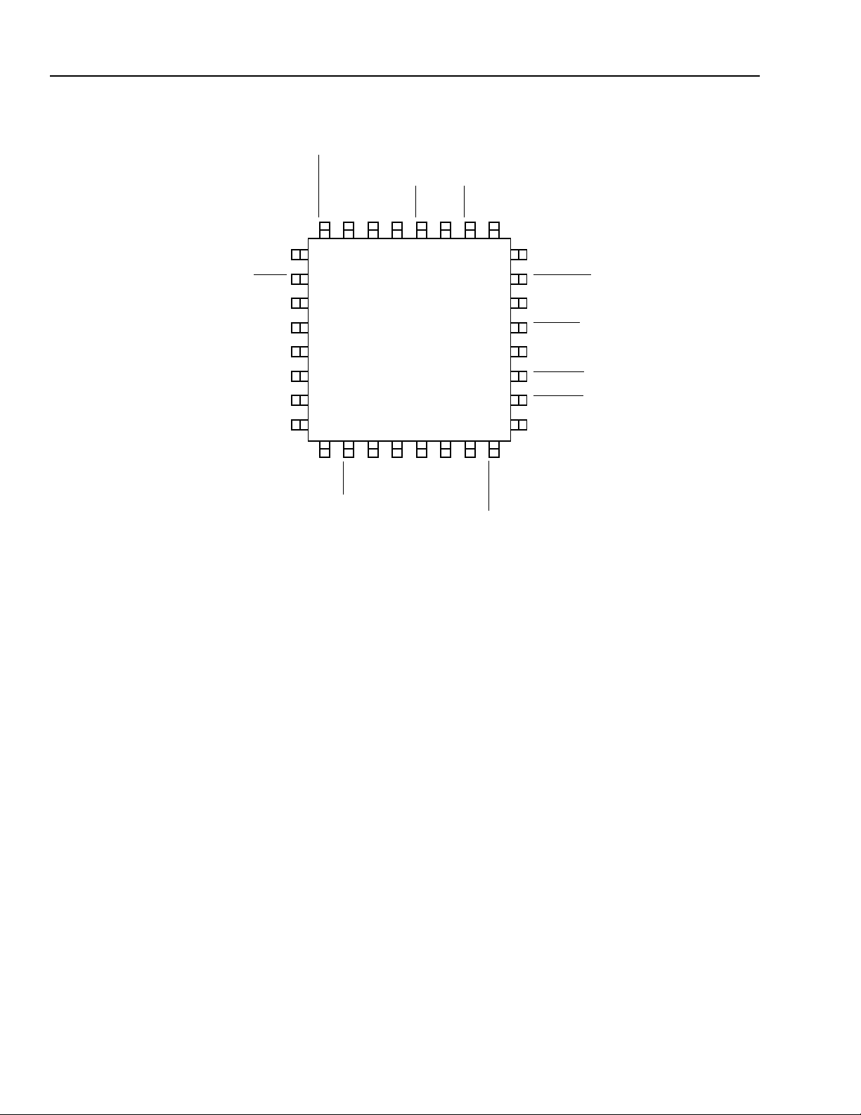
V
RESET
SEL[4]
SEL[3]
SEL[2]
SEL[1]
SEL[0]
DDA
V
PLL_BYPASS
24 1723 22 21 20 19 18
25
SS
26
27
28
29
30
31
32
18234567
DDD
V
DDPECL
PLLREF_EN
V
SS
V
TESTM
PCLK0
PCLK0
PCLK1
PCLK0_EN
REF_SEL
PCLK1_EN
DDPECL
PCLK1
V
EXTFB_OUT
16
EXTFB_OUT
15
V
PECL_CLK
9
DDPECL
EXTFB_IN
EXTFB_IN
EXTFB_EN
PECL_CLK
PECL_CLK
2275 (F)
14
13
12
11
10
PECL_CLK
Figure 2. 32-Pin TQFP
2 Agere Systems Inc.
Preliminary Data Sheet
July 2001
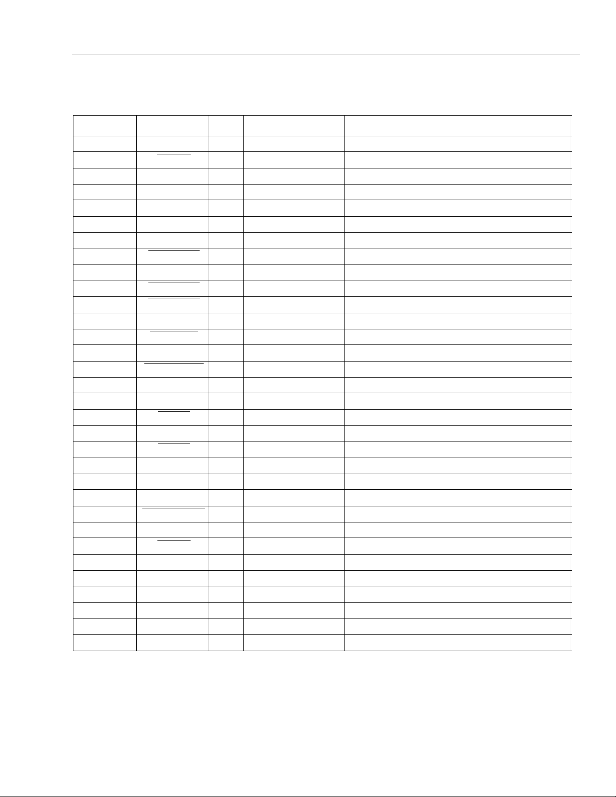
Pin Information
Table 1. Pin Description
Pin Number Pin Name
I/O
LCK4802
Low-Voltage PECL Differential Clock
1
Type Description
1V
DDD
2TESTM
3V
SS
P Power Supply 3.3 V power supply.
I LVCMOS M divider test pins.
G Ground Digital ground.
4 PCLK0_EN I LVCMOS PCLK0 enable.
5 PCLK1_EN I LVCMOS PCLK1 enable.
6 REF_SEL I LVCMOS Selects the PLL input reference clock.
7 PECL_CLK I Differential PECL PLL reference clock input.
8 PECL_CLK
I Differential PECL PLL reference clock input.
9 PECL_CLK I Differential LVPECL PLL reference clock input.
10 PECL_CLK
11 EXTFB_EN
I Differential LVPECL PLL reference clock input.
I LVCMOS External feedback enable.
12 EXTFB_IN I Differential PECL External feedback input.
13 EXTFB_IN
14 V
DDPECL
15 EXTFB_OUT
I Differential PECL External feedback input.
P Power Supply Output buffers power supply.
O Differential PECL External feedback output clock.
16 EXTFB_OUT O Differential PECL External feedback output clock.
17 V
DDPECL
18 PCLK1
P Power Supply Output buffers power supply.
O Differential PECL Output clock 1.
19 PCLK1 O Differential PECL Output clock 1.
20 PCLK0
O Differential PECL Output clock 0.
21 PCLK0 O Differential PECL Output clock 0.
22 VDDPECL
P Power Supply Output buffers power supply.
23 PLLREF_EN I LVCMOS PLL reference enable.
24 PLL_BYPASS
25 V
SS
26 RESET
I LVCMOS Input signal PLL bypass.
P Ground Analog ground for PLL.
I LVCMOS PLL bypass reset (for test use).
27 SEL[4] I LVCMOS Selection of input and feedback frequency.
28 SEL[3] I LVCMOS Selection of input and feedback frequency.
29 SEL[2] I LVCMOS Selection of input and feedback frequency.
30 SEL[1] I LVCMOS Selection of input and feedback frequency.
31 SEL[0] I LVCMOS Selection of input and feedback frequency.
32 V
1. P = power, I = input, G = ground, O = output.
DDA
P Power Supply 3.3 V filtered for PLL (PLL power supply).
Agere Systems Inc. 3
 Loading...