

AGERE LCK4801 Datasheet
LCK4801
Low-Voltage HSTL Differential Clock
Preliminary Data Sheet
July 2001
General
The LCK4801 is a low-voltage, 3.3 V HSTL
differential clock synthesizer. The LCK4801 supports
two differential HSTL output pairs with frequencies
from 336 MHz to 1 GHz. The clock is designed to
support single and multip le proces so r systems that
require HSTL differential inputs. The LCK4801
contains a fully integrated PLL (phase-locked loop)
which multiplies the HSTL_CLK or PECL_CLK input
frequency to match individual processor clock
frequencies. The PLL can be bypassed so that the
PCLK outputs are fed from the HSTL_CLK or
PECL_CLK input for test purposes. All outputs are
powered from a 2 V external supply to reduce onchip power consumption. All outputs are HSTL. The
PLL can operate in the internal feedback mode, or in
the external feedback mode for board level
debugging applications.
Description
Features
■
Two fully selectable clock inputs.
■
Fully integrated PLL.
■
336 MHz to 1 GHz output frequencies.
■
HSTL outputs.
■
HSTL and LVPECL reference clocks.
■
32-pin TQFP package.
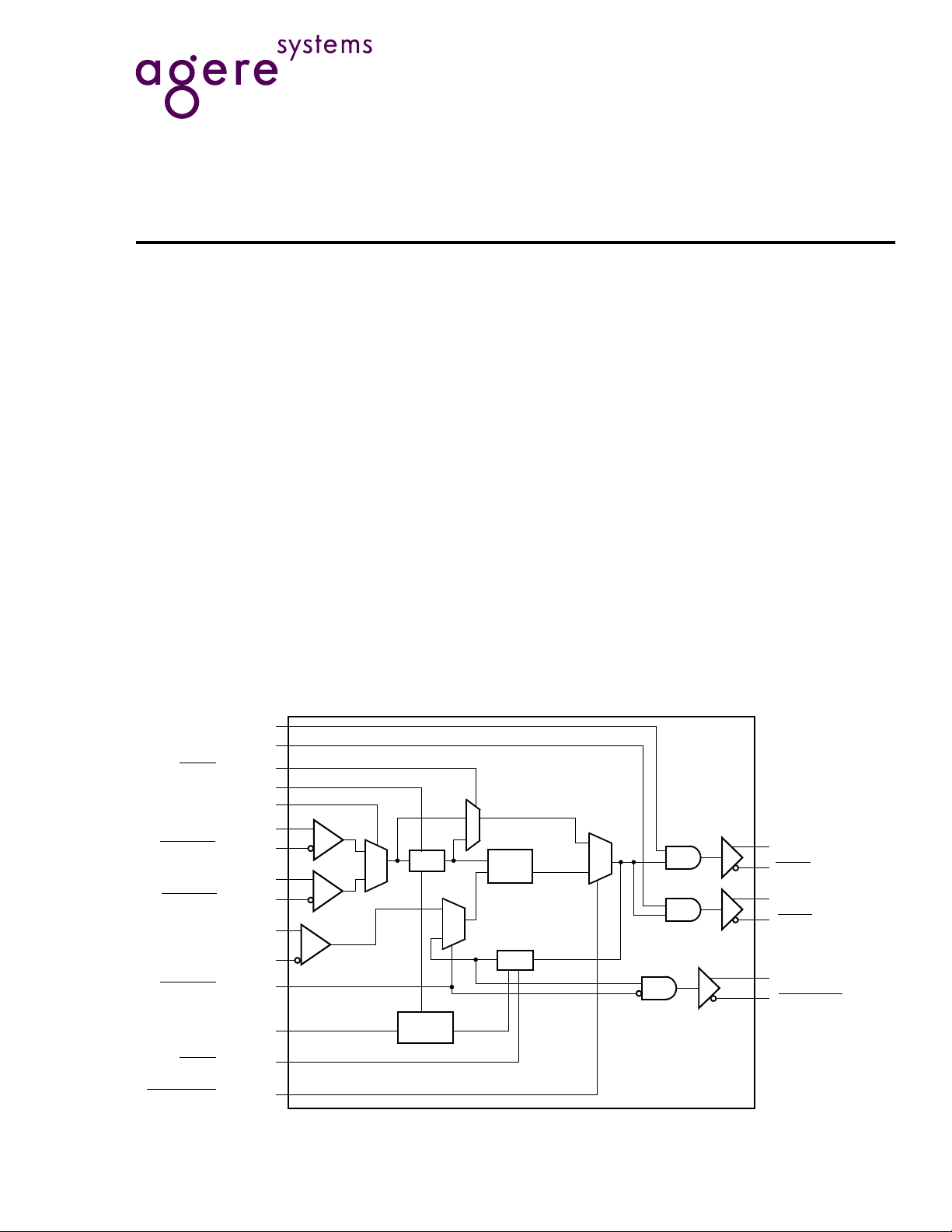
PCLK0_EN (PULL-UP)
PCLK1_EN (PULL-UP)
TESTM
(PULL-UP)
PLLREF_EN (PULL-UP)
REF_SEL (PULL-UP)
HSTL_CLK (PULL-UP)
HSTL_CLK
PECL_CLK (PULL-UP)
PECL_CLK
EXTFB_EN
PLL_BYPASS
(PULL-UP)
(PULL-UP)
(PULL-UP)
EXTFB_IN (HSTL)
(PULL-DOWN)
(PULL-UP)
SEL[4:0] (PULL-UP)
(PULL-UP)
RESET
(PULL-UP)
1
0
1
/M
DECODE
0
PLL
0
1
/N
Figure 1. LCK4801 Logic Diagram
0
1
PCLK0
PCLK0
(HSTL)
PCLK1
(HSTL)
PCLK1
EXTFB_OUT
EXTFB_OUT
(HSTL)
2274.a (F)

LCK4801
Low-Voltage HSTL Differential Clock
Preliminary Data Sheet
July 2001
Description
(continued)
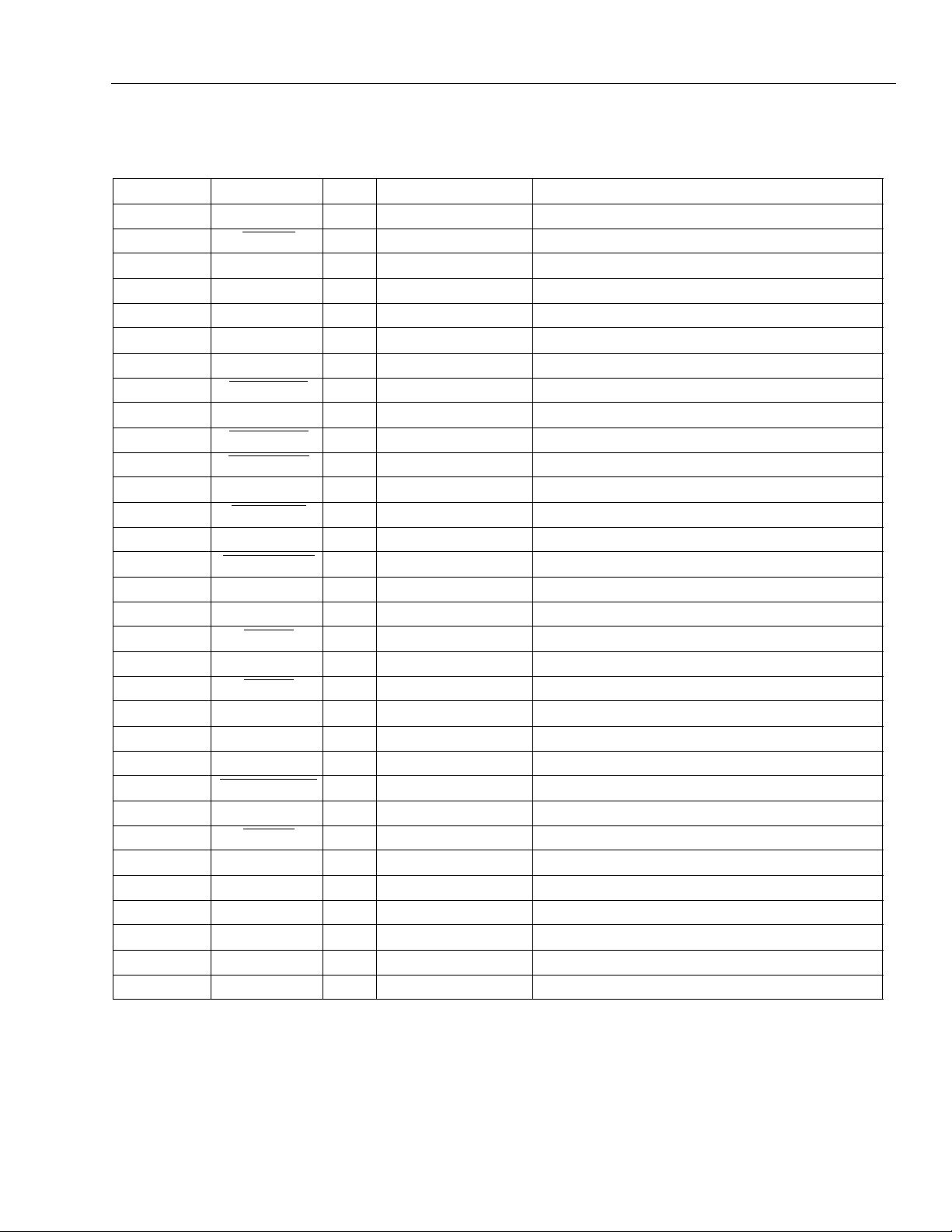
V
RESET
SEL[4]
SEL[3]
SEL[2]
SEL[1]
SEL[0]
DDA
V
PLL_BYPASS
24 1723 22 21 20 19 18
25
SS
26
27
28
29
30
31
32
18234567
DDD
V
DDHSTL
PLLREF_EN
V
SS
V
TESTM
PCLK0
PCLK0
PCLK1
PCLK0_EN
REF_SEL
PCLK1_EN
DDHSTL
PCLK1
V
EXTFB_OUT
16
EXTFB_OUT
15
V
HSTL_CLK
9
DDHSTL
EXTFB_IN
EXTFB_IN
EXTFB_EN
PECL_CLK
PECL_CLK
2275 (F)
14
13
12
11
10
HSTL_CLK
Figure 2. 32-Pin TQFP
2 Agere Systems Inc.
Preliminary Data Sheet
July 2001
Pin Information
Table 1. Pin Description
LCK4801
Low-Voltage HSTL Differential Clock
Pin Number Pin Name I/O
1V
DDD
2TESTM
3V
SS
1
Type Description
P Power Supply 3.3 V power supply.
I LVCMOS M divider test pins.
G Ground Digital ground.
4 PCLK0_EN I LVCMOS PCLK0 enable.
5 PCLK1_EN I LVCMOS PCLK1 enable.
6 REF_SEL I LVCMOS Selects the PLL input reference clock.
7 HSTL_CLK I Differential HSTL PLL reference clock input.
8HSTL_CLK
I Differential HSTL PLL reference clock input.
9 PECL_CLK I Differential LVPECL PLL reference clock input.
10 PECL_CLK
11 EXTFB_EN
I Differential LVPECL PLL reference clock input.
I LVCMOS External feedback enable.
12 EXTFB_IN I Differential HSTL External feedback input.
13 EXTFB_IN
14 V
DDHSTL
15 EXTFB_OUT
I Differential HSTL External feedback input.
P Power Supply Output buffers power supply.
O Differential HSTL External feedback output clock.
16 EXTFB_OUT O Differential HSTL External feedback output clock.
17 VDDHSTL
18 PCLK1
P Power Supply Output buffers power supply.
O Differential HSTL Output clock 1.
19 PCLK1 O Differential HSTL Output clock 1.
20 PCLK0
O Differential HSTL Output clock 0.
21 PCLK0 O Differential HSTL Output clock 0.
22 V
DDHSTL
P Power Supply Output buffers power supply.
23 PLLREF_EN I LVCMOS PLL reference enable.
24 PLL_BYPASS
25 V
SS
26 RESET
I LVCMOS Input signal PLL bypass.
P Ground Analog ground for PLL.
I LVCMOS PLL bypass reset (for test use).
27 SEL[4] I LVCMOS Selection of input and feedback frequency.
28 SEL[3] I LVCMOS Selection of input and feedback frequency.
29 SEL[2] I LVCMOS Selection of input and feedback frequency.
30 SEL[1] I LVCMOS Selection of input and feedback frequency.
31 SEL[0] I LVCMOS Selection of input and feedback frequency.
32 V
1. P = power, I = input, G = ground, O = output.
DDA
P Power Supply 3.3 V filtered for PLL (PLL power supply).
Agere Systems Inc. 3
 Loading...