

AGERE FW801A-DB Datasheet

FW801A Low-Power PHY IEEE 1394A-2000
One-Cable Transceiver/Arbiter Device
Supports connection debounce.
Distinguishing Features
■
Compliant with IEEE Standard 1394a-2000,
IEEE Standard for a High Performance Serial
Bus Amendment 1.
Low power consumption during powerdown or
■
microlow-power sleep mode.
Supports extended BIAS_HANDSHAKE time for
■
enhanced interoperability with camcorders.
While unpowered and connected to the bus, will
■
not drive TPBIAS on the connected port even if
receiving incoming bias voltage on the port.
Does not require external filter capacitors for PLL.
■
Does not require a separate 5 V supply for 5 V link
■
controller interoperability.
Interoperable across 1394 cable with 1394 physi-
■
cal layers (PHY) using 5 V supplies.
Interoperable with 1394 link-layer controllers using
■
5 V supplies.
1394a-2000 compliant common mode noise filter
■
on incoming TPBIAS.
Powerdown features to conserve energy in bat-
■
tery-powered applications include:
— Device powerdown pin.
— Link interface disable using LPS.
— Inactive ports power down.
— Automatic microlow-power sleep mode during
suspend.
Interface to link-layer controller supports Annex J
■
electrical isolation as well as bus-keeper isolation.
Features
Provides one fully compliant cable port at
■
100 Mbits/s, 200 Mbits/s, and 400 Mbits/s.
Fully supports OHCI requirements.
■
Supports arbitrated short bus reset to improve
■
utilization of the bus.
Supports ack-accelerated arbitration and fly-by
■
concatenation.
■
Supports multispeed packet concatenation.
■
Supports PHY pinging and remote PHY access
■
packets.
Fully supports suspend/resume.
■
Supports PHY-link interface initialization and reset.
■
Supports 1394a-2000 register set.
■
Supports LPS/link-on as a part of PHY-link inter-
■
face.
Supports provisions of IEEE 1394-1995 Standard
■
for a High Performance Serial Bus.
Fully interoperable with FireWire† implementation
■
of IEEE 1394-1995.
Reports cable power fail interrupt when voltage at
■
CPS pin falls below 7.5 V.
Separate cable bias and driver termination voltage
■
supply for the port.
Meets Intel‡ Mobile Power Guideline 2000.
■
Other Features
48-pin TQFP package.
■
Single 3.3 V supply operation.
■
Data interface to link-layer controller provided
■
through 2/4/8 parallel lines at 50 Mbits/s.
25 MHz crystal oscillator and PLL provide transmit/
■
receive data at 100 Mbits/s, 200 Mbits/s, and
400 Mbits/s, and link-layer controller clock at
50 MHz.
Node power-class information signaling for system
■
power management.
Multiple separate package signals provided for
■
analog and digital supplies and grounds.
* IEEE is a registered trademark of The Institute of Electrical and
Electronics Engineers, Inc.
† FireWire is a registered trademark of Apple Computer, Inc.
‡ Intel is a registered trademark of Intel Corporation.
Data Sheet, Rev. 1
June 2001

FW801A Low-Power PHY IEEE 1394A-2000 Data Sheet, Rev. 1
One-Cable Transceiver/Arbiter Device June 2001
Table of Contents
Contents Page
Distinguishing Features ............................................................................................................................................ 1
Features ...................................................................................................................................................................1
Other Features ......................................................................................................................................................... 1
Description ................................................................................................................................................................3
Signal Information ..................................................................................................................................................... 6
Application Information ........................................................................................................................................... 10
Crystal Selection Considerations ............................................................................................................................ 11
1394 Application Support Contact Information ....................................................................................................... 12
Absolute Maximum Ratings .................................................................................................................................... 12
Electrical Characteristics ........................................................................................................................................13
Timing Characteristics ............................................................................................................................................ 16
Timing Waveforms .................................................................................................................................................. 17
Internal Register Configuration ............................................................................................................................... 18
Outline Diagrams ....................................................................................................................................................23
Ordering Information ...............................................................................................................................................23
List of Figures
Figures Page
Figure 1. Block Diagram ........................................................................................................................................... 5
Figure 2. Pin Assignments ........................................................................................................................................ 6
Figure 3. Typical External Component Connections ..............................................................................................10
Figure 4. Typical Port Termination Network ........................................................................................................... 11
Figure 5. Dn, CTLn, and LREQ Input Setup and Hold Times Waveforms ............................................................. 17
Figure 6. Dn, CTLn Output Delay Relative to SYSCLK Waveforms .......................................................................17
List of Tables
Table s Page
Table 1. Signal Descriptions ..................................................................................................................................... 7
Table 2. Absolute Maximum Ratings ......................................................................................................................12
Table 3. Analog Characteristics .............................................................................................................................. 13
Table 4. Driver Characteristics ............................................................................................................................... 14
Table 5. Device Characteristics ..............................................................................................................................15
Table 6. Switching Characteristics ......................................................................................................................... 16
Table 7. Clock Characteristics ................................................................................................................................16
Table 8. PHY Register Map for the Cable Environment ........................................................................................18
Table 9. PHY Register Fields for the Cable Environment ...................................................................................... 18
Table 10. PHY Register Page 0: Port Status Page ................................................................................................ 20
Table 11. PHY Register Port Status Page Fields ................................................................................................... 21
Table 12. PHY Register Page 1: Vendor Identification Page .................................................................................22
Table 13. PHY Register Vendor Identification Page Fields .................................................................................... 22
2 Agere Systems Inc.

Data Sheet, Rev. 1 FW801A Low-Power PHY IEEE 1394A-2000
June 2001 One-Cable Transceiver/Arbiter Device
Description
The Agere Systems Inc. FW801A device provides the
analog physical layer functions needed to implement a
one-port node in a cable-based IEEE 1394-1995 and
IEEE 1394a-2000 network.
The cable port incorporates two differential line transceivers. The transceivers include circuitry to monitor
the line conditions as needed for determining connection status, for initialization and arbitration, and for
packet reception and transmission. The PHY is
designed to interface with a link-layer controller (LLC).
The PHY requires either an external 24.576 MHz crystal or crystal oscillator. The internal oscillator drives an
internal phase-locked loop (PLL), which generates the
required 400 MHz reference signal. The 400 MHz reference signal is internally divided to provide the
49.152 MHz, 98.304 MHz, and 196.608 MHz clock signals that control transmission of the outbound encoded
strobe and data information. The 49.152 MHz clock
signal is also supplied to the associated LLC for synchronization of the two chips and is used for resynchronization of the received data. The powerdown function,
when enabled by the PD signal high, stops operation of
the PLL and disables all circuitry except the cable-notactive signal circuitry.
The PHY supports an isolation barrier between itself
and its LLC. When /ISO is tied high, the link interface
outputs behave normally. When /ISO is tied low,
internal differentiating logic is enabled, and the outputs
become short pulses, which can be coupled through a
capacitor or transformer as described in the
IEEE 1394-1995 Annex J. To operate with bus-keeper
isolation, the /ISO pin of the FW801A must be tied
high.
Data bits to be transmitted through the cable ports are
received from the LLC on two, four, or eight data lines
(D[0:7]), and are latched internally in the PHY in
synchronization with the 49.152 MHz system clock.
These bits are combined serially, encoded, and
transmitted at 98.304 Mbits/s, 196.608 Mbits/s, or
393.216 Mbits/s as the outbound data-strobe
information stream. During transmission, the encoded
data information is transmitted differentially on the TPA
and TPB cable pair(s).
During packet reception, the TPA and TPB
transmitters of the receiving cable port are disabled,
and the receivers for that port are enabled. The
encoded data information is received on the TPA and
TPB cable pair. The received data-strobe information
is decoded to recover the receive clock signal and the
serial data bits. The serial data bits are split into two,
four, or eight parallel streams, resynchronized to the
local system clock, and sent to the associated LLC.
The received data is also transmitted (repeated) out of
the other active (connected) cable ports.
Both the TPA and TPB cable interfaces incorporate
differential comparators to monitor the line states
during initialization and arbitration. The outputs of
these comparators are used by the internal logic to
determine the arbitration status. The TPA channel
monitors the incoming cable common-mode voltage.
The value of this common-mode voltage is used during
arbitration to set the speed of the next packet
transmission. In addition, the TPB channel monitors
the incoming cable common-mode voltage for the
presence of the remotely supplied twisted-pair bias
voltage. This monitor is called bias-detect.
The TPBIAS circuit monitors the value of incoming
TPA pair common-mode voltage when local TPBIAS is
inactive. Because this circuit has an internal current
source and the connected node has a current sink, the
monitored value indicates the cable connection status.
This monitor is called connect-detect.
Both the TPB bias-detect monitor and TPBIAS
connect-detect monitor are used in suspend/resume
signaling and cable connection detection.
The PHY provides a 1.86 V nominal bias voltage for
driver load termination. This bias voltage, when seen
through a cable by a remote receiver, indicates the
presence of an active connection. The value of this
bias voltage has been chosen to allow interoperability
between transceiver chips operating from 5 V or 3 V
nominal supplies. This bias voltage source should be
stabilized by using an external filter capacitor of
approximately 0.33 µF.
The transmitter circuitry, the receiver circuitry, and the
twisted-pair bias voltage circuity are all disabled with a
powerdown condition. The powerdown condition
occurs when the PD input is high. The port transmitter
circuitry, the receiver circuitry, and the TPBIAS output
are also disabled when the port is disabled,
suspended, or disconnected.
The line drivers in the PHY operate in a highimpedance current mode and are designed to work
with external 112 Ω line-termination resistor networks.
One network is provided at each end of each twistedpair cable. Each network is composed of a pair of
series-connected 56 Ω resistors. The midpoint of the
pair of resistors that is directly connected to the
twisted-pair A (TPA) signals is connected to the
Agere Systems Inc. 3

FW801A Low-Power PHY IEEE 1394A-2000 Data Sheet, Rev. 1
One-Cable Transceiver/Arbiter Device June 2001
Description
TPBIAS voltage signal. The midpoint of the pair of
resistors that is directly connected to the twisted-pair B
(TPB) signals is coupled to ground through a parallel
RC network with recommended resistor and capacitor
values of 5 kΩ and 220 pF, respectively.
The value of the external resistors are specified to
meet the standard specifications when connected in
parallel with the internal receiver circuits.
The driver output current, along with other internal
operating currents, is set by an external resistor. This
resistor is connected between the R0 and R1 signals
and has a value of 2.49 kΩ ± 1%.
The FW801A supports suspend/resume as defined in
the IEEE 1394a-2000 specification. The suspend
mechanism allows the FW801A port to be put into a
suspended state. In this state, the port is unable to
transmit or receive data packets, however, it remains
capable of detecting connection status changes and
detecting incoming TPBias. When the FW801A port is
suspended, all circuits except the bias voltage
reference generator, and bias detection circuits are
powered down, resulting in significant power savings.
The use of suspend/resume is recommended.
The signal, C/LKON, as an input, indicates whether a
node is a contender for bus manager. When the
C/LKON signal is asserted, it means the node is a contender for bus manager. When the signal is not
asserted, it means that the node is not a contender.
The C bit corresponds to bit 20 in the self-ID packet
(see Table 4-29 of the IEEE 1394-1995 standard for
additional details).
The power-class bits of the self-ID packet do not have
a default value. These bits can be initialized and read/
written through the LLC using Figure 6-1 (PHY Register Map) of the IEEE 1394a-2000 standard. See Table
8 for the address space of the Pwr_class register.
A powerdown signal (PD) is provided to allow a powerdown mode where most of the PHY circuits are
powered down to conserve energy in battery-powered
applications. The internal logic in FW801A is reset as
long as the powerdown signal is asserted. A cable status signal, CNA, provides a high output when none of
the twisted-pair cable ports are receiving incoming
bias voltage. This output is not debounced. The CNA
output can be used to determine when to power the
PHY down or up. In the powerdown mode, all circuitry
is disabled except the CNA circuitry. It should be noted
that when the device is powered down, it does not act
in a repeater mode.
(continued)
When the power supply of the PHY is removed while
the twisted-pair cables are connected, the PHY transmitter and receiver circuitry has been designed to
present a high impedance to the cable in order to not
load the TPBIAS signal voltage on the other end of the
cable.
For reliable operation, the TPBn signals must be terminated using the normal termination network regardless
of whether a cable is connected to a port or not connected to a port. When the port does not have a cable
connected, internal connect-detect circuitry will keep
the port in a disconnected state.
Note: All gap counts on all nodes of a 1394 bus must
be identical. This may be accomplished by using
PHY configuration packets (see Section 4.3.4.3
of IEEE 1394-1995 standard) or by using two
bus resets, which resets the gap counts to the
maximum level (3Fh).
The link power status (LPS) signal works with the
C/LKON signal to manage the LLC power usage of the
node. The LPS signal indicates that the LLC of the
node is powered up or powered down. If LPS is inactive for more than 1.2 µs and less than 25 µs, PHY/link
interface is reset. If LPS is inactive for greater than
25 µs, the PHY will disable the PHY/link interface to
save power. If the PHY then receives a link-on packet,
the C/LKON signal is activated to output a 6.114 MHz
signal, which can be used by the LLC to power itself
up. Once the LLC is powered up, the LPS signal communicates this to the PHY and the PHY/link interface
is enabled. C/LKON signal is turned off when LPS is
active or when a bus reset occurs, provided the interrupt that caused C/LKON is not present.
When the PHY/link interface is in the disabled state,
the FW801A will automatically enter a low-power
mode, if all ports are inactive (disconnected, disabled,
or suspended). In this low-power mode, the FW801A
disables its PLL and also disables parts of reference
circuitry depending on the state of the ports (some reference circuitry must remain active in order to detect
incoming TP bias). The lowest power consumption (the
microlow-power sleep mode) is attained when all ports
are either disconnected or disabled with the ports interrupt enable bit cleared. The FW801A will exit the lowpower mode when the LPS input is asserted high or
when a port event occurs that requires the FW801A to
become active in order to respond to the event or to
notify the LLC of the event (e.g., incoming bias or disconnection is detected on a suspended port, a new
connection is detected on a nondisabled port, etc.).
4 Agere Systems Inc.
Data Sheet, Rev. 1 FW801A Low-Power PHY IEEE 1394A-2000
June 2001 One-Cable Transceiver/Arbiter Device
Description
(continued)
The SYSCLK output will become active (and the PHY/
link interface will be initialized and become operative)
within 3 ms after LPS is asserted high, when the
FW801A is in the low-power mode.
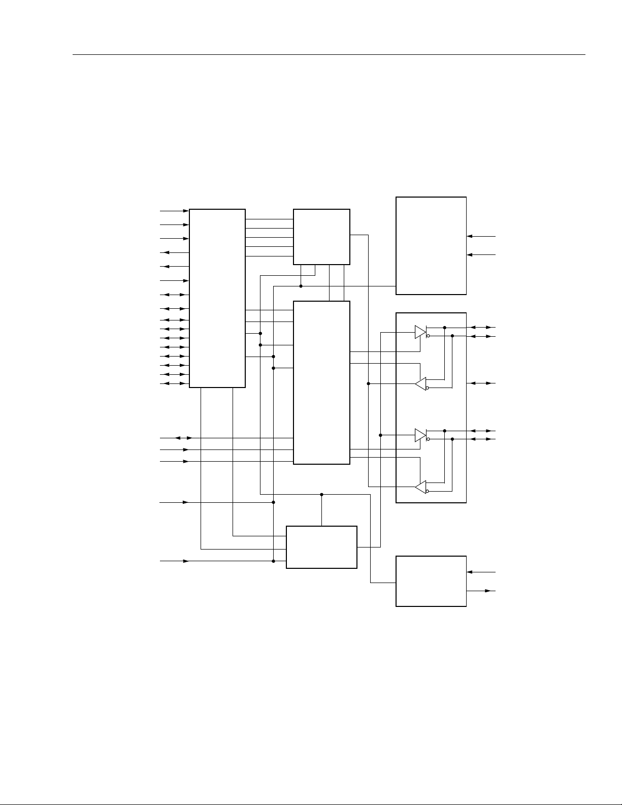
CPS
LPS
/ISO
CNA
SYSCLK
LREQ
CTL0
CTL1
D0
D1
D2
D3
D4
D5
D6
D7
LINK
INTERFACE
I/O
RECEIVED
DATA
DECODER/
RETIMER
ARBITRATION
CONTROL
STATE
MACHINE
LOGIC
Two of the signals are used to set up various test conditions used in manufacturing. These signals (SE and
SM) should be connected to V
BIAS
VOLTAGE
AND
CURRENT
GENERATOR
AND
CABLE PORT 0
SS
for normal operation.
R0
R1
TPA0+
TPA0–
TPBIAS0
C/LKON
SE
SM
PD
/RESET
TRANSMIT
DATA
ENCODER
Figure 1. Block Diagram
CRYSTAL
OSCILLATOR,
PLL SYSTEM,
AND
CLOCK
GENERATOR
TPB0+
TPB0–
XI
XO
5-5459.e (F)r.2
Agere Systems Inc. 5
FW801A Low-Power PHY IEEE 1394A-2000 Data Sheet, Rev. 1
One-Cable Transceiver/Arbiter Device June 2001
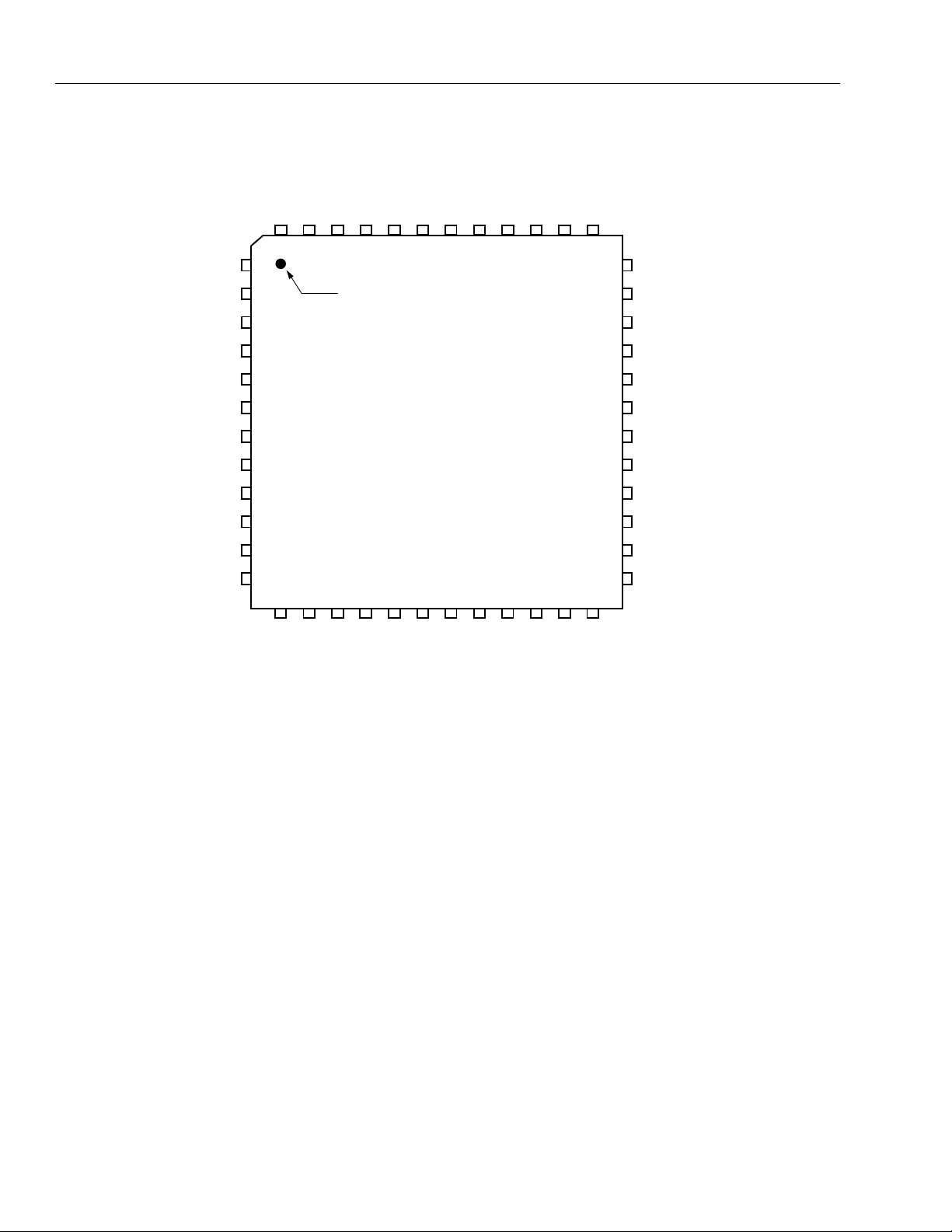
Signal Information
DD
SS
DD
PLLV
41
SS
V
40
V
39
R1
38
R0
37
36
V
SSA
CTL0
LREQ
48
SS
V
47
SYSCLK
46
/RESET
45
XO
44
XI
43
PLLV
42
1
CTL1
2
3
D0
4
D1
5
V
DD
6
D2
PIN #1 IDENTIFIER
AGERE FW801A
7
D3
8
D4
9
D5
10
D6
11
D7
12
V
SS
13
14
15
16
CNA
17
SS
DD
V
LPS
V
18
PD
19
/ISO
20
CPS
21
SS
V
22
DD
V
23
SE
C/LKON
Note: Active-low signals are indicated by “/” at the beginning of signal names, within this document.
35
34
33
32
31
30
29
28
27
26
25
24
SM
V
SSA
V
DDA
V
DDA
TPBIAS0
TPA0+
TPA0–
TPB0+
TPB0–
V
SSA
V
SSA
V
DDA
5-7302.a (F) R.03
Figure 2. Pin Assignments
6 Agere Systems Inc.

Data Sheet, Rev. 1 FW801A Low-Power PHY IEEE 1394A-2000
June 2001 One-Cable Transceiver/Arbiter Device
Signal Information
Table 1. Signal Descriptions
Pin Signal* Type Name/Description
17 C/LKON I/O Bus Manager Capable Input and Link-On Output. On hardware reset,
13 CNA O Cable-Not-Active Output. CNA is asserted high when none of the PHY
20 CPS I Cable Power Status. CPS is normally connected to the cable power
1 CTL0 I/O Control I/O. The CTLn signals are bidirectional communications control
2CTL1
3, 4, 6, 7,
8, 9, 10,
11
19 /ISO I Link Interface Isolation Disable Input (Active-Low). /ISO controls the
D[0:7] I/O Data I/O. The Dn signals are bidirectional and pass data between the
(continued)
this pin is used to set the default value of the contender status indicated
during self-ID. The bit value programming is done by tying the signal
through a 10 kΩ resistor to V
(low, not bus manager capable). Using either the pull-up or pull-down
resistor allows the link-on output to override the input value when necessary.
After hardware reset, this pin is set as an output.
C/LKON indicates one of the following events by asserting a 6.114 MHz
signal.
1. FW801A receives a link-on packet addressed to this node.
2. Port_event register bit is 1.
3. Any of the Timeout, Pwr_Fail, or Loop register bits are 1 and the
Resume_int register bit is also 1. Once activated, the C/LKON output will
continue active until the LPS becomes active. The PHY also deasserts
the C/LKON output when a bus reset occurs, if the C/LKON is active due
solely to the reception of a link-on packet.
Note:
ports are receiving an incoming bias voltage. This circuit remains active
during the powerdown mode.
through a 400 kΩ resistor. This circuit drives an internal comparator that
detects the presence of cable power. This information is maintained in
one internal register and is available to the LLC by way of a register read
(see Table 8, Register 0).
signals between the PHY and the LLC. These signals control the passage
of information between the two devices. Bus-keeper circuitry is built into
these terminals.
PHY and the LLC. Bus-keeper circuitry is built into these terminals.
operation of an internal pulse differentiating function used on the PHYLLC interface signals, CTLn and Dn, when they operate as outputs. When
/ISO is asserted low, the isolation barrier is implemented between PHY
and its LLC (as described in Annex J of IEEE 1394-1995). /ISO is normally tied high to disable isolation differentiation. Bus-keepers are
enabled when /ISO is high (inactive) on CTL, D, and LREQ. When /
ISO is low (active), the bus-keepers are disabled. Please refer to Agere’s
application note AP98-074CMPR for more information on isolation.
If an interrupt condition exists which would otherwise cause the C/
LKON output to be activated if the LPS were inactive, the C/LKON
output will be activated when the LPS subsequently becomes inactive.
DD (high, bus manager capable) or to GND
If the LPS is inactive,
* Active-low signals are indicated by “/ ” at the beginning of signal names, within this document.
Agere Systems Inc. 7

FW801A Low-Power PHY IEEE 1394A-2000 Data Sheet, Rev. 1
One-Cable Transceiver/Arbiter Device June 2001
Signal Information
(continued)
Table 1. Signal Descriptions (continued)
Pin Signal* Type Name/Description
DD
14 LPS I Link Power Status. LPS is connected to either the V
supplying the
LLC or to a pulsed output that is active when the LLC is powered for the
purpose of monitoring the LLC power status. If LPS is inactive for more
than 1.2 µs and less than 25 µs, interface is reset. If LPS is inactive for
greater than 25 µs, the PHY will disable the PHY/Link interface to save
power. FW801A continues its repeater function.
48 LREQ I Link Request. LREQ is an output from the LLC that requests the PHY to
perform some service. Bus-keeper circuitry is built into this terminal.
18 PD I Powerdown. When asserted high, PD turns off all internal circuitry except
the bias-detect circuits that drive the CNA signal. Internal FW801A logic is
kept in the reset state as long as PD is asserted. PD terminal is provided
for backward compatibility. It is recommended that the FW801A be
allowed to manage its own power consumption using suspend/resume in
conjunction with LPS. C/LKON features are defined in 1394a-2000.
41 PLLV
DD — Power for PLL Circuit. PLLVDD
supplies power to the PLL circuitry
portion of the device.
42 PLLV
SS — Ground for PLL Circuit. PLLVSS is tied to a low-impedance ground
plane.
37 R0 I Current Setting Resistor. An internal reference voltage is applied to a
resistor connected between R0 and R1 to set the operating current and
38 R1
the cable driver output current. A low temperature-coefficient resistor
(TCR) with a value of 2.49 kΩ ± 1% should be used to meet the
IEEE 1394-1995 standard requirements for output voltage limits.
45 /RESET I
Reset (Active-Low).
is reset. An internal pull-up resistor, which is connected to V
When /RESET is asserted low (active), the FW801A
DD
, is provided,
so only an external delay capacitor is required. This input is a standard
logic buffer and can also be driven by an open-drain logic output buffer.
23 SE I
24 SM I
46 SYSCLK O
Test Mode Control.
be tied to V
SS
Test Mode Control.
be tied to V
SS
System Clock.
SE is used during the manufacturing test and should
.
SM is used during the manufacturing test and should
.
SYSCLK provides a 49.152 MHz clock signal, which is
synchronized with the data transfers to the LLC.
31 TPA0+ Analog I/O
Portn, Port Cable Pair A.
TPAn is the port A connection to the twisted-pair
cable. Board traces from each pair of positive and negative differential
signal pins should be kept matched and as short as possible to the external
load resistors and to the cable connector.
30 TPA0− Analog I/O
Portn, Port Cable Pair A.
TPAn is the port A connection to the twisted-pair
cable. Board traces from each pair of positive and negative differential
signal pins should be kept matched and as short as possible to the external
load resistors and to the cable connector.
29 TPB0+ Analog I/O
Portn, Port Cable Pair B.
TPBn is the port B connection to the twisted-pair
cable. Board traces from each pair of positive and negative differential
signal pins should be kept matched and as short as possible to the external
load resistors and to the cable connector.
* Active-low signals are indicated by “/ ” at the beginning of signal names, within this document.
8 Agere Systems Inc.
 Loading...