

AGERE FW322 Datasheet

Data Sheet, Rev. 1
February 2001
1394A PCI PHY/Link Open Host Controller Interface
Features
■
1394a-2000 OHCI link and PHY core function in single device:
— Enables smaller, simpler, more efficient mother-
board and add-in card designs by replacing two
components with one
— Enables lower system costs
— Leverages proven 1394a-2000 PHY core design
— Demonstrated compatibility with current Microsoft
Windows* drivers and common applications
— Demonstrated interoperability with existing, as well
as older, 1394 consumer electronics and periph-
erals products
— Feature-rich implementation for high performance
in common applications
— Supports low-power system designs (CMOS
implementation, power management features)
— Provides LPS, LKO N, and CNA outputs to support
legacy power management implementations
■
OHCI:
— Complies with 1394 OHCI specification
revision 1.0
— Supports the following 1394 OHCI revision 1.1
features:
❑
Isochronous receive dual-buffer mode.
❑
Enhanced isochronous transmit skip/overflow
support.
❑
ack_data_error improvememnts for asynchronous and physical requests.
❑
Enhanced CSR control register implementation.
❑
Autonomous configuration ROM updates.
❑
Enhanced power management support,
including ack_tardy event.
❑
Enhanced SelfID protocol, including
selfIDComplete2 event.
— Compatible with Microsoft OHCI, DV, and SBP-2
driver stack in W98, W98SE, W2000, and
MacOS
— 4 Kbyte isochronous transmit FIFO
— 2 Kbyte asynchronous transmit FIFO
— 4 Kbyte isochronous receive FIFO
— 2 Kbyte asychronous receive FIFO
— Dedicated asynchronous and isochronous
descriptor-based DMA engines
— Eight isochronous transmit contexts
— Eight isochronous receive contexts
— Prefetches isochronous transmit data
— Supports posted write transactions
†
operating system
FW322
■
1394a-2000 PHY core:
— Compliant with IEEE
High Performance Serial Bus (S upplement)
— Provides two fully compliant cable ports each
supporting 400 Mbits/s, 200 Mbits/s, and
100 Mbits/s traffic
— Supports extended BIAS_HANDSHAKE time for
enhanced interoperability with camcorders
— While unpowered and connected to the bus, will
not drive TPBIAS on a connected port even if
receiving incoming bias voltage on that port
— Does not require external filter capacitor for PLL
— Supports PHY core-link interface initialization and
reset
— Supports link-on as a part of the internal
PHY core-link interface
— 25 MHz crystal oscillator and internal PLL provide
transmit/receive data at 100 Mbits/s, 200 Mbits/s,
and 400 Mbits/s, and internal link-layer controller
clock at 50 MHz
— Interoperable across 1394 cable with 1394 phys-
ical layers (PHY core) using 5 V supplies
— Node power-class information signaling for
system power management
— Supports ack-accelerated arbitration and fly-by
concatenation
— Supports arbitrated short bus reset to improve
utilization of the bus
— Fully supports suspend/resume
— Supports connection debounce
— Supports multispeed packet concatenation
— Supports PHY pinging and remote PHY access
packets
— Reports cable power fail interrupt when voltage at
CPS pin falls below 7.5 V
— Separate cable bias and driver termination voltage
supply for each port
■
Link:
— Cycle master and isochronous resource manager
capable
— Supports 1394a-2000 acceleration features
* Microsoft and Windows are registered trademarks of Microsoft
Corporation.
† MacOS is a registered trademark of Apple Computer, Inc.
‡ IEEE is a registered trademark of The Institute of Electrical and
Electronics Engineers, Inc.
‡
1394a-2000, Standard for a

FW322 Data Sheet, Rev. 1
1394A PCI PHY/Link Op en Host Controller Interface February 2001
Table of Contents
Contents Page
Features ...................................................................................................................................................................1
FW322 Functional Overview ....................................................................................................................................7
Other Features .........................................................................................................................................................7
FW322 Functional Description .................................................................................................................................7
PCI Core ............................................................................................................................................................7
Isochronous Data Transfer ................................................... ....... ...... ...... ....... ...... ....... ...... ..... ...........................8
Asynchronous Data Transfer ......... ....... ...... ....... ...... ....... ...... ....... ...... ...... ..........................................................8
Asynchronous Register ...................................................................... ................................................................8
Link Core ............................................................................................................................................................9
PHY Core ...........................................................................................................................................................9
Pin Information .......................................................................................................................................................12
Application Schematic ............................................................................................................................................17
Internal Registers ...................................................................................................................................................19
PCI Configuration Registers ............................................................................................................................19
Vendor ID Register ..........................................................................................................................................20
Device ID Register ...........................................................................................................................................21
PCI Command Register ...................................................................................................................................22
PCI Status Register .........................................................................................................................................24
Class Code and Revision ID Register ..............................................................................................................25
Latency Timer and Class Cache Line Size Register ........................................................................................26
Header Type and BIST Register ......................................................................................................................27
OHCI Base Address Register ..........................................................................................................................29
PCI Subsystem Identification Register .............................................................................................................31
PCI Power Management Capabilities Pointer Register ....................................................................................31
Interrupt Line and Pin Register ........................................................................................................................32
MIN_GNT and MAX_LAT Register ..................................................................................................................33
PCI OHCI Control Register ..............................................................................................................................34
Capability ID and Next Item Pointer Register ..................................................................................................36
Power Management Capabilities Register .......................................................................................................37
Power Management Control and Status Register ............................................................................................39
Power Management Extension Register ..........................................................................................................41
OHCI Registers ................................................................................................................................................42
OHCI Version Register ....................................................................................................................................45
GUID ROM Register ........................................................................................................................................47
Asynchronous Transmit Retries Register .........................................................................................................49
CSR Data Register ..........................................................................................................................................51
CSR Compare Register ...................................................................................................................................53
CSR Control Register ......................................................................................................................................55
Configuration ROM Header Register ...............................................................................................................57
Bus Identification Register ...............................................................................................................................59
Bus Options Register .......................................................................................................................................61
GUID High Register .........................................................................................................................................63
GUID Low Register ..........................................................................................................................................65
Configuration ROM Mapping Register .............................................................................................................67
Posted Write Address Low Register ................................................................................................................69
Posted Write Address High Register ...............................................................................................................71
Vendor ID Register ..........................................................................................................................................73
Host Controller Control Register ......................................................................................................................75
Self-ID Count Register .....................................................................................................................................79
Isochronous Receive Channel Mask High Register .........................................................................................81
Isochronous Receive Channel Mask Low Register ..........................................................................................83
2 Lucent Technologies Inc.

Data Sheet, Rev. 1 FW322
February 2001 1394A PCI PHY/Link Open Host Controller Interface
Table of Contents
(continued)
Contents Page
Interrupt Event Register ...................................................................................................................................85
Interrupt Mask Register ....................................................................................................................................88
Isochronous Transmit Interrupt Event Register ................................................................................................90
Isochronous Transmit Interrupt Mask Register ................................................................................................92
Isochronous Receive Interrupt Event Register ... ...... ....... ...... ...... ....... ...... ....................................... .................93
Isochronous Receive Interrupt Mask Register ...................... ...... ....... ...... ....... ...... ....... ...... ..............................95
Fairness Control Register ................................................................................................................................96
Link Control Register ........................................................................................................................................98
Node Identification Register ...........................................................................................................................100
PHY Core Layer Control Register ..................................................................................................................102
Isochronous Cycle Timer Register .................................................................................................................104
Asynchronous Request Filter High Register ..................................................................................................106
Asynchronous Request Filter Low Register ...................................................................................................109
Physical Request Filter High Register ............................................................................................................112
Physical Request Filter Low Register ............................................................................................................115
Asynchronous Context Control Register ........................................................................................................118
Asynchronous Context Command Pointer Register .......................................................................................120
Isochronous Transmit Context Control Register ............................................................................................122
Isochronous Transmit Context Command Pointer Register ...........................................................................124
Isochronous Receive Context Control Regi ster .............. ...... ...... ....... ...... ....... ...............................................126
Isochronous Receive Context Command Pointer Register ............................................................................128
Isochronous Receive Context Match Register ...................................................... ....... ...... ....... ...... ...............130
FW322 Vendor-Specific Registers .................................................................................................................132
Isochronous DMA Control ........................................................... ....... ............................................................133
Asynchronous DMA Control ...........................................................................................................................134
Link Options ...................................................................................................................................................135
Crystal Selection Considerations ..........................................................................................................................137
Load Capacitance ..........................................................................................................................................137
Board Layout ..................................................................................................................................................137
Electrical Characteristics ......................................................................................................................................138
Timing Characteristics ..........................................................................................................................................140
Internal Register Configuration .............................................................................................................................141
PHY Core Register Map for Cable Environment ............................................................................................141
PHY Core Register Fields for Cable Environment .........................................................................................142
Outline Diagrams ..................................................................................................................................................147
120-Pin TQFP ................................................................................................................................................147
Figure Page
Figure 1. FW322 Functional Block Diagram .............................................................................................................7
Figure 2. PHY Core Block Diagram ........................................................................................................................11
Figure 3. Pin Assignments for FW322 ....................................................................................................................12
Figure 4. Application Schematic for FW322 ...........................................................................................................18
Lucent Technologies Inc. 3

FW322 Data Sheet, Rev. 1
1394A PCI PHY/Link Op en Host Controller Interface February 2001
Table of Contents
(continued)
Table Page
Table 1. Pin Descriptions ....................................................................................................................................... 13
Table 2. Bit-Field Access Tag Description ............................................................................................................. 19
Table 3. PCI Configuration Register Map .............................................................................................................. 19
Table 4. Vendor ID Register .................................................................................................................................. 20
Table 5. Device ID Register ................................................................................................................................... 21
Table 6. PCI Command Register ........................................................................................................................... 22
Table 7. PCI Command Register Description ........................................................................................................ 23
Table 8. PCI Status Register ................................................................................................................................. 24
Table 9. Class Code and Revision ID Register .................................................................................................... 25
Table 10. Class Code and Revision ID Register Description ................................................................................ 26
Table 11. Latency Timer and Class Cache Line Size Register ............................................................................. 26
Table 12. Latency Timer and Class Cache Line Size Register Description ......................................................... 27
Table 13. Header Type and BIST Register ........................................................................................................... 27
Table 14. Header Type and BIST Register Description ........................................................................................ 28
Table 15. OHCI Base Address Register ................................................................................................................ 29
Table 16. OHCI Base Address Register Description ............................................................................................. 30
Table 17. PCI Subsystem Identification Register Description ............................................................................... 31
Table 18. PCI Power Management Capabilities Pointer Register ......................................................................... 31
Table 19. Interrupt Line and Pin Register .............................................................................................................. 32
Table 20. Interrupt Line and Pin Register Description ........................................................................................... 32
Table 21. MIN_GNT and MAX_LAT Register ........................................................................................................ 33
Table 22. MIN_GNT and MAX_LAT Register Description ..................................................................................... 33
Table 23. PCI OHCI Control Register ................................................................................................................... 34
Table 24. PCI OHCI Control Register Description ................................................................................................. 35
Table 25. Capability ID and Next Item Pointer Register ........................................................................................ 36
Table 26. Capability ID and Next Item Pointer Register Description ..................................................................... 36
Table 27. Power Management Capabilities Register ............................................................................................ 37
Table 28. Power Management Capabilities Register Description ......................................................................... 38
Table 29. Power Management Control and Status Register ................................................................................ 39
Table 30. Power Management Control and Status Register Description .............................................................. 40
Table 31. Power Management Extension Register ............................................................................................... 41
Table 32. Power Management Extension Register Description ........................................................................... 41
Table 33. OHCI Register Map ............................................................................................................................... 42
Table 34. OHCI Version Register .......................................................................................................................... 45
Table 35. OHCI Version Register Description ....................................................................................................... 46
Table 36. GUID ROM Register ............................................................................................................................. 47
Table 37. GUID ROM Register Description ........................................................................................................... 48
Table 38. Asynchronous Transmit Retries Register ............................................................................................. 49
Table 39. Asynchronous Transmit Retries Register Description ........................................................................... 50
Table 40. CSR Data Register ................................................................................................................................ 51
Table 41. CSR Data Register Description ............................................................................................................. 52
Table 42. CSR Compare Register ......................................................................................................................... 53
Table 43. CSR Compare Register Description ...................................................................................................... 54
Table 44. CSR Control Register ............................................................................................................................ 55
Table 45. CSR Control Register Description ........................................................................................................ 56
Table 46. Configuration ROM Header Register ..................................................................................................... 57
Table 47. Configuration ROM Header Register Description ................................................................................. 58
Table 48. Bus Identification Register ..................................................................................................................... 59
Table 49. Bus Identification Register Description .................................................................................................. 60
Table 50. Bus Options Register ............................................................................................................................. 61
Table 51. Bus Options Register Description .......................................................................................................... 62
44 Lucent Technologies Inc.

Data Sheet, Rev. 1 FW322
February 2001 1394A PCI PHY/Link Open Host Controller Interface
Table of Contents
(continued)
Table Page
Table 52. GUID High Register ............................................................................................................................... 63
Table 53. GUID High Register Description ............................................................................................................ 64
Table 54. GUID Low Register ................................................................................................................................ 65
Table 55. GUID Low Register Description ............................................................................................................. 66
Table 56. Configuration ROM Mapping Register ................................................................................................... 67
Table 57. Configuration ROM Mapping Register Description ................................................................................ 68
Table 58. Posted Write Address Low Register ...................................................................................................... 69
Table 59. Posted Write Address Low Register Description ................................................................................... 70
Table 60. Posted Write Address High Register ..................................................................................................... 71
Table 61. Posted Write Address High Register Description .................................................................................. 72
Table 62. Vendor ID Register ................................................................................................................................ 73
Table 63. Vendor ID Register Description ............................................................................................................. 74
Table 64. Host Controller Control Register ............................................................................................................ 75
Table 65. Host Controller Control Register Description ......................................................................................... 76
Table 66. Self-ID Buffer Pointer Register .............................................................................................................. 77
Table 67. Self-ID Buffer Pointer Register Description ........................................................................................... 78
Table 68. Self-ID Count Register ........................................................................................................................... 79
Table 69. Self-ID Count Register Description ........................................................................................................ 80
Table 70. Isochronous Receive Channel Mask High Register .............................................................................. 81
Table 71. Isochronous Receive Channel Mask High Register Description ...........................................................82
Table 72. Isochronous Receive Channel Mask Low Register ............................................................................... 83
Table 73. Isochronous Receive Channel Mask Low Register Description ...........................................................84
Table 74. Interrupt Event Register ......................................................................................................................... 85
Table 75. Interrupt Event Register Description ...................................................................................................... 86
Table 76. Interrupt Mask Register ......................................................................................................................... 88
Table 77. Interrupt Mask Register Description ...................................................................................................... 89
Table 78. Isochronous Transmit Interrupt Event Register ..................................................................................... 90
Table 79. Isochronous Transmit Interrupt Event Register Description .................................................................. 91
Table 80. Isochronous Transmit Interrupt Mask Register ...................................................................................... 92
Table 81. Isochronous Receive Interrupt Event Register ...................................................................................... 93
Table 82. Isochronous Receive Interrupt Event Description ................................................................................. 94
Table 83. Isochronous Receive Interrupt Mask Register ....................................................................................... 95
Table 84. Fairness Control Register ...................................................................................................................... 96
Table 85. Fairness Control Register Description ................................................................................................... 97
Table 86. Link Control Register ............................................................................................................................ 98
Table 87. Link Control Register Description ......................................................................................................... 99
Table 88. Node Identification Register ................................................................................................................ 100
Table 89. Node Identification Register Description ............................................................................................. 101
Table 90. PHY Core Layer Control Register ....................................................................................................... 102
Table 91. PHY Core Layer Control Register Description .................................................................................... 103
Table 92. Isochronous Cycle Timer Register ...................................................................................................... 104
Table 93. Isochronous Cycle Timer Register Description ................................................................................... 105
Table 94. Asychronous Request Filter High Register ......................................................................................... 106
Table 95. Asynchronous Request Filter High Register Description ..................................................................... 107
Table 96. Asynchronous Request Filter Low Register ....................................................................................... 109
Table 97. Asynchronous Request Filter Low Register Description ..................................................................... 110
Table 98. Physical Request Filter High Register ................................................................................................. 112
Table 99. Physical Request Filter High Register Description .............................................................................. 113
Table 100. Physical Request Filter Low Register ............................................................................................... 115
Table 101. Physical Request Filter Low Register Description ............................................................................. 116
Table 102. Asynchronous Context Control Register ........................................................................................... 118
Lucent Technologies Inc. 5

FW322 Data Sheet, Rev. 1
1394A PCI PHY/Link Op en Host Controller Interface February 2001
Table of Contents
(continued)
Table Page
Table 103. Asynchronous Context Control Register Description ....................................................................... 119
Table 104. Asynchronous Context Command Pointer Register ......................................................................... 120
Table 105. Asynchronous Context Command Pointer Register Description ....................................................... 121
Table 106. Isochronous Transmit Context Control Register ................................................................................ 122
Table 107. Isochronous Transmit Context Control Register Description ............................................................ 123
Table 108. Isochronous Transmit Context Command Pointer Register .............................................................. 124
Table 109. Isochronous Transmit Context Command Pointer Register Description ........................................... 125
Table 110. Isochronous Receive Context Control Register ................................................................................. 126
Table 111. Isochronous Receive Context Control Register Description .............................................................. 127
Table 112. Isochronous Receive Context Command Pointer Register ............................................................... 128
Table 113. Isochronous Receive Context Command Pointer Register Description ............................................ 129
Table 114. Isochronous Receive Context Match Register .................................................................................. 130
Table 115. Isochronous Receive Context Match Register Description ............................................................... 131
Table 116. FW322 Vendor-Specific Registers Description ................................................................................. 132
Table 117. Isochronous DMA Control Registers Description .............................................................................. 133
Table 118. Asynchronous DMA Control Registers Description ........................................................................... 134
Table 119. Link Registers Description ................................................................................................................. 135
Table 120. ROM Format Description ................................................................................................................... 136
Table 121. Analog Characteristics ....................................................................................................................... 138
Table 122. Driver Characteristics ........................................................................................................................ 139
Table 123. Device Characteristics ....................................................................................................................... 139
Table 124. Switching Characteristics .................................................................................................................. 140
Table 125. Clock Characteristics ......................................................................................................................... 140
Table 126. PHY Core Register Map for the Cable Environment ......................................................................... 141
Table 127. PHY Core Register Fields for Cable Environment ............................................................................. 142
Table 128. PHY Core Register Page 0: Port Status Page .................................................................................. 144
Table 129. PHY Core Register Port Status Page Fields .................................................................................... 145
Table 130. PHY Core Register Page 1: Vendor Identification Page ................................................................... 146
Table 131. PHY Core Register Vendor Identification Page Fields ...................................................................... 146
66 Lucent Technologies Inc.
Data Sheet, Rev. 1 FW322
February 2001 1394A PCI PHY/Link Open Host Controller Interface
FW322 Functional Overview
PCI:
■
— Revision 2.2 compliant
— 33 MHz/32-bit operation
— Programmable burst size for PCI data transfer
— Supports PCI Bus Power Management Interface specification v.1.1
— Supports clockrun protocol per PCI Mobile Design Guide
— Global byte swap function
Other Features
I2C serial ROM interface
■
CMOS process
■
3.3 V operation, 5 V tolerant inputs
■
120-pin TQFP package
■
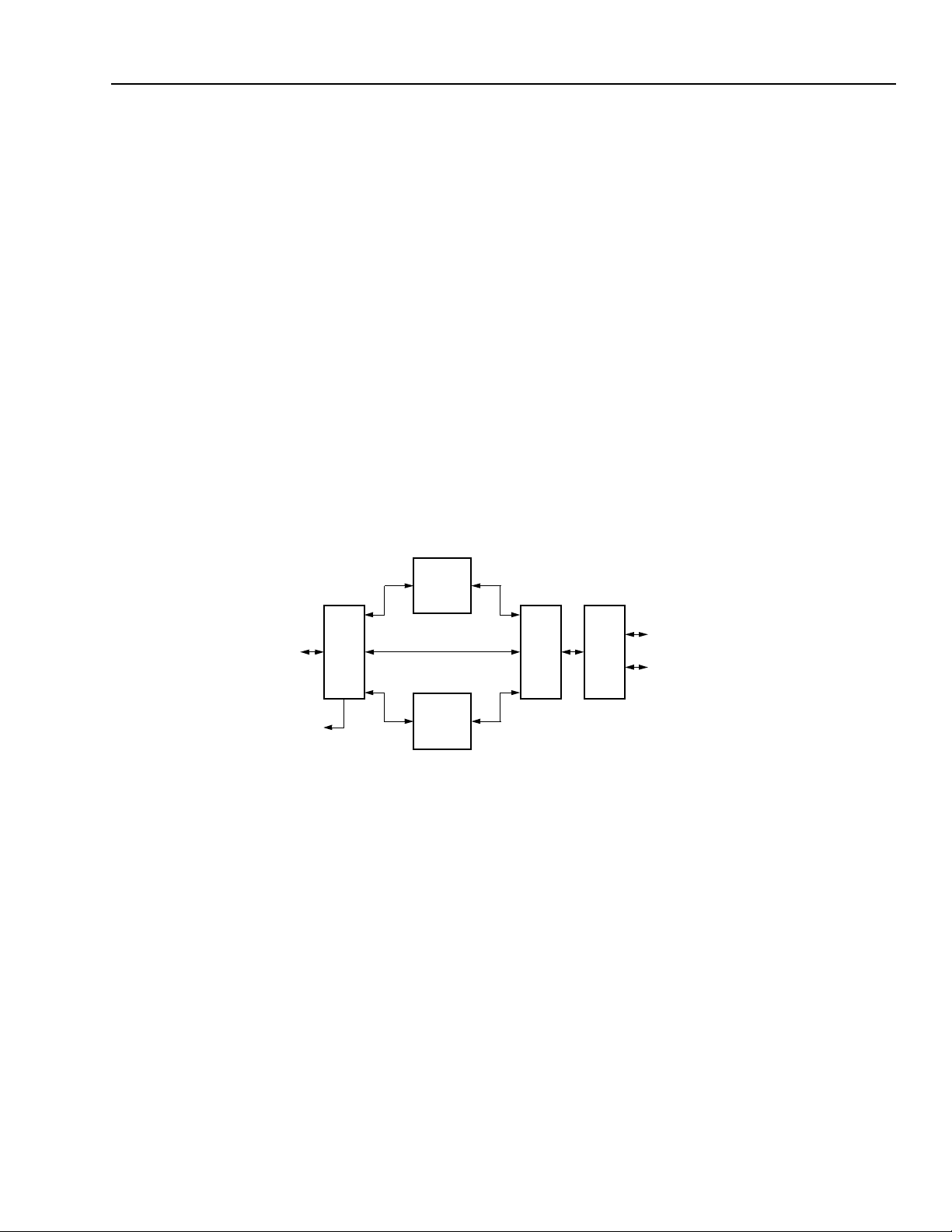
The FW322 is the Lucent Technologies Microelectronics Group implementation of a high-performance, PCI busbased open host controller for implementation of
tions are handled by the FW322 , uti lizing the on-chip 1394 a-200 0 com pliant link co re a nd ph ysical layer core. A hi ghperformance and cost-effective solution for connecting and servicing multiple
1394a-2000) peripheral devices can be realized.
IEEE
1394a-2000 compliant systems and devices. Link-layer func-
IEEE
1394 (both 1394-1995 and
OHCI
ASYNC
PCI
BUS
ROM
I/F
PCI
CORE
OHCI
ISOCH
Figure 1. FW322 Functional Block Diagram
FW322 Functional Description
The FW322 is comprised of five major functional sections (see Figure 1): PCI core, isochronous data transfer, asynchronous data transfer, link core, and PHY
core. The following is a general description of each of
the five major sections.
PCI Core
The PCI core serves as the interface to the PCI bus. It
contains the state machines that allow the F W322 to
respond properly wh en it is t he target o f t he transa ction .
During 1394 packet transmission or reception, the PCI
core arbitrates for the PCI bus and enables the FW322
LINK
CORE
PHY
CORE
CABLE PORT 1
CABLE PORT 0
5-6250 (F)f
to become the bus master for reading the different
buffer descriptors and management of the actual data
transfers to/from host system memory.
The PCI core also supports th e PCI Bus Power
Management Interface specification v.1.1. Included in
this support is a standard power management register
interface accessible through the PCI configuration
space. Through this register interface, software is able
to transition the FW322 into four distinct power
consumption states (D0, D1, D2, and D3). This permits
software to selectively increase/decrease the power
consumption of th e FW 322 for r ea sons such a s pe ri o ds
of system inactivity or power conservation. In addition,
the FW322 also includ es su ppo r t fo r hardware wake-up
mechanisms through power management events
(PMEs). When the FW322 is in a low-power state,
Lucent Technologies Inc. 7

FW322 Data Sheet, Rev. 1
1394A PCI PHY/Link Op en Host Controller Interface February 2001
FW322 Functional Description
PMEs pro vide a hardware mechanism for requ esting a
software wake-up. Together, the power management
register interface and PME support within the FW322
combine to form an efficient means for implementing
power management.
(continued)
Isochronous Data Transfer
The isochronous data tr ansf er log ic handles the tr ansf er
of isochronous data between the link core and the PCI
interface module. It consists of the isochronous registe r
module, the isochronous transmit DMA module, the
isochronous receive DMA module, the isochronous
transmit FIFO, and the isochronous receive FIFO.
Isochronous Register
The isochronous register module operates on PCI slave
accesses to OHCI registers within the isochronous
block. The module also maintains the status of interrupts generated w ithin the isoc hronous b lock and send s
the isochronous interrupt status to the OHCI interrupt
handler block.
Isochronous Transmit DMA (ITDMA)
The isochronous transmit DMA module moves data
from host memory to the link core, which will then send
the data to the 1394 bus. It consists of isochronous
contexts, each of which is independently controlled by
software, and can send data on a 1394 isochronous
channel.
During each 1394 isochronous cycle, the ITDMA
module will serv ice each of the contexts and attempt to
process one 1394 pack et f or each cont ext. If a con tex t is
active, ITDMA will request acce ss to the PCI b us . When
granted PCI access, a descriptor block is fetched from
host memory. This data is decoded by ITDMA to determine how much data is required and where in host
memory the data resides. ITDMA initiates another PCI
access to fetch this data, which is placed into the
transmit FIFO for processing by the link core. If the
context is not active, it is skipped by ITDMA for the
current cycle.
After processing each context, ITDMA writes a cycle
marker word in the transmit FIFO to indicate to the link
core that there is no more data for this isochronous
cycle.
As a summary, the major steps for the FW322 ITDMA to
transmit a packet are the following:
1. Fetch a descriptor block from host memory.
2. Fetch data specified by the descriptor block from
host memory, and place it into the isochronous
transmit FIFO.
3. Data in FIFO is read by the link and sent to the PHY
core device interface.
Isochronous Receive DMA (IRDMA)
The isochronous re ceiv e DMA modu le mo ves data from
the receive FIFO to host memory. It consists of isochronous contexts, each of which is independently
controlled by software. Normally, each context can
process data on a single 1394 isochronous channel.
However, software can select one context to receive
data on multipl e chann el s.
When IRDMA detects t hat the link core ha s p la ced da ta
into the receive FIFO, it immediately reads out the first
word in the FIFO, which makes up the header of the
isochronous packet. IRDMA extracts the channel
number for the packet and packet filtering controls from
the header. This information is compared with the
control registers for each context to determine if any
context is to process this packet.
If a match is found, IRDMA will request access to the
PCI bus. When granted PCI access, a descriptor block
is fetched from host memory. The descriptor provides
information about the host memory block allocated for
the incoming pack et. IRDMA th en reads the pac ket from
the receive F IFO and writes the data to host me mory via
the PCI bus.
If no match is found, IRDMA will read the remainder of
the packet from the receive FIFO, but not process the
data in any way.
Asynchronous Data Transfer
The ASYNC block is functionally partitioned into two
independent logic blocks for transmitting and receiving
1394 packets. The ASYNC_TX unit is responsible for
packet transmission while the ASYNC_RX unit processes received data.
Asynchronous Register
The asynchronous register module operates on PCI
slave accesses to OHCI registers within the asynchronous block. The module also maintains the status ofinterrupts generated within the asynchronous block and
8 Lucent Technologies Inc.

Data Sheet, Rev. 1 FW322
February 2001 1394A PCI PHY/Link Open Host Controller Interface
FW322 Functional Description
sends the asynchronous interrupt status to the OHCI
interrupt handler block.
Asynchronous Transmit (ASYNC_TX)
The ASYNC_TX block of the FW322 manages the
asynchronous transmission of either request or
response packets. The mechanism for asynchronous
transmission of requests and responses are similar.
The only difference is the system memory location of
the buffer descriptor list when processing the two contexts. Therefore, the discussion below, which is for
asynchronous transmit requests, parallels that of the
asynchronous transmit response. The FW322 asynchronous transmission of packets involves the following
steps:
1. Fetch complete buffer descriptor block from host
memory.
2. Get data from system memory and store into
async FIFO.
3. Request transfer of data from FIFO to link device.
4. Handle retr ies, if any.
5. Handle errors in steps 1 to 4.
6. End the transfer if there are no errors.
Asynchronous Receive (ASYNC_RX)
The ASYNC_RX bl ock of the FW322 manages the
processing of received packets. Data packe ts are
parsed and stored in a ded icated asynchro nous re ceive
FIFO. Command descriptors are read through the PCI
interface to determine the disposition of the data
arriving through the 1394 li n k.
The header of the received packet is processed to
determine, among other things, the following:
1. The type of packet received.
2. The source and destinations.
3. The data and size, if any.
4. The operation r equire d, if an y. For e xamp le, co mpare
and sw ap ope r a ti on .
The ASYNC block also handles DMA transfers of selfID packets during the 1394 bus initialization phase and
block transactions associated with physical request.
(continued)
Link Core
It is the responsibility of the link to ascertain if a
received packet is to be forwarded to the OHCI for
processing. If so, the packet is directed to a proper
inbound FIFO for either the isochronous block or the
asynchronous block to process. The link is also
responsible for CRC generation on outgoing packets
and CRC checking on receivi ng packets.
To become aware of data to be sent outbound on
1394 bus, the link must monitor the OHCI FIFOs looking for packets in need of transmission. Based on data
received from the OHCI block, the link will form packet
headers for the 1394 bus. The link will alert the PHY
core as to the availability of the outbound data. It is the
link’s function to generate CRC for the outbound data.
The link also provides PHY core register access for the
OHCI.
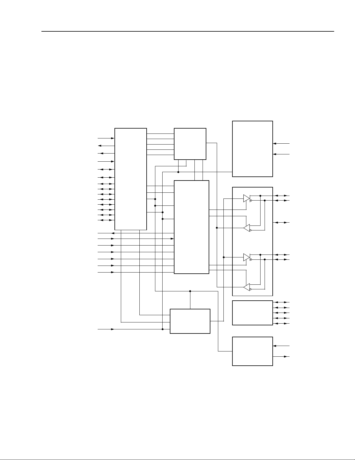
PHY Core
The PHY core provides the analog physical layer functions needed to implement a two-port node in a cable-
IEEE
based
Each cable port incorporates two differential line trans-
ceivers. The transceivers include circuitry to monitor the
line conditions as needed for determining connection
status, for initialization and arbitration, and for packet
reception and transmission. The PHY core interfaces
with the link core.
The PHY core requires either an external 24.576 MHz
crystal or crystal oscillator. The internal oscillator drives
an internal phase-locked loop (PLL), which generates
the required 400 MHz reference s ignal. The 400 M Hz
reference signal is internally divided to provide the
49.152 MHz, 98.304 MHz, and 196.608 MHz clock signals that cont rol transmission of the outbou nd encoded
strobe and data information. The 49.152 MHz clock signal is also supplied to the associated LLC for
synchronization of the two chips and is used for resynchronization of the received data.
The PHY/link interface is a direct connection and does
not provide is olation.
Data bits to be transmitted through the cable ports are
received from the LLC on two, four, or eight data lines
(D[0:7]), and are latched internally in the PHY in synchronization with the 49.152 MHz system clock. These
bits are combined serially, encoded, and transmitted at
98.304 Mbits/s, 196.608 Mbits/s, or 393.216 Mbits/s as
the outbound data-strobe information stream. During
transmission, the encoded data information is transmitted differentially on the TPA and TPB cable pair(s).
During packet reception, the TPA and TPB transmitters
of the receiving cable port are disabled, and the receivers for that port are enabled. The encoded data
information is received on the TPA and TPB cable pair.
The received data-strobe information is decoded to
1394-1995 and
IEEE
1394a-2000 network.
Lucent Technologies Inc. 9

FW322 Data Sheet, Rev. 1
1394A PCI PHY/Link Op en Host Controller Interface February 2001
FW322 Functional Description
recover the receive cl ock si g nal and the serial d ata b it s.
The serial data bits are split into two, four, or eight parallel streams, resynchronized to the local system clock,
and sent to the associated LLC. The received data is
also transmitted (repeated) out of the other active (connected) cabl e ports.
Both the TPA and TPB cable int erfaces incorporate
differential comparators to monitor the line states during
initialization and arbitr a tion. The outputs of these
comparators are used by the internal logic to determine
the arbitration status. The TPA channel monitors the
incoming cable common-mode voltage. The value of
this common-mode voltage is used during arbitration to
set the speed of the next packet transmission. In
addition, the TPB channel monitors the incoming cable
common-mode voltage for the presence of the remotely
supplied twisted-pair bias voltage. This monitor is called
bias-detect.
The TPBIAS circuit monitors the value of in com ing TPA
pair common-mode voltage wh en local TPBIAS is
inactive. Because this circuit has an internal current
source and the connected node has a current sink, the
monitored valu e indicates the cable connection status.
The monitor is called connect- detect.
Both the TPB bias-detect monitor and TPBIAS connectdetect monitor are used in suspend/resume signaling
and cable connection detection.
The PHY core provides a 1.86 V nominal bias voltage
for driver load termination. This bias voltage, when
seen through a cable by a remote recei ver , indi cate s
the presence of an active connection. The value of this
bias voltage has been chosen to allow interopera bility
between transceiver chips operating from 5 V or 3 V
nominal supplies. This bias voltage source should be
stabilized by using an external filter capacitor of
approximately 0.33 µF.
The port transmitter circuitry and the receiver circuitry
are disabled when the port is disabled, suspended, or
disconnected.
The line drivers in the PHY core operate in a highimpedance current m ode an d are designe d to w ork w ith
external 112 Ω line-termination resistor networks. One
network is provided at each end of each twisted-pair
cable. Each network is composed of a pair of seriesconnected 56 Ω resistors. The midpoint of the pair of
resistors that is directly connected to the twisted-pair A
(TPA) signals is connected to the TPBIAS voltage
signal. The midpoint of the pair of resistors that is
directly connected to the twiste d-pair B (TPB) signals is
coupled to ground through a parallel RC network with
recommended resistor and capacitor values of 5 kΩ
(continued)
and 220 pF, respectively. The value of the external
resistors are specified to meet the draft standard
specifications when connected in parallel with the
internal receiver circuits.
The driver output current, along with other internal
operating currents, is set by an external resistor. This
resistor is connected between the R0 and R1 signals
and has a value of 2.49 kΩ ±1%.
Four signals are used as i nputs to se t four co nfigur ation
status bits in the self-identification (self-ID) pa cket.
These signal s are hardwired high or low as a function
of the equipment design. PC[0:2] are the three signals
that indicate eit her t he need for power f ro m the cab l e o r
the ability to supply power to the cable. The fourth
signal (CONTENDER) as an input indicates whether a
node is a contender for bus manager. When the
CONTENDER signal is asserted, it means the node is a
contender for bus manager. When the signal is not
asserted, it means that the node is not a contender.
The contender bit corresponds to bit 20 in th e self-ID
packet, PC0 corresponds to bit 21, PC1 corresponds to
bit 22, and PC2 corresponds to bit 23 (see Table 4-29
IEEE
of the
When the power supply of the PHY core is removed
while the twisted-pair cables are connected, the PHY
core transmitter and receiver circuitry has been
designed to present a high impedance to the cable in
order to not load the TPBIAS signal voltage on the
other end of the cable.
For reliable operation, the TPBn signals must be
terminated using the normal termination netw ork
regardless of whether a cable is connected to port or
not connected to a port. For those applications, when
FW322 is used with one or more of the ports not
brought out to a connector, those unused ports may be
left unconnected without normal termination. When a
port does not have a cable connected, internal connectdetect circuitry will keep the port in a disconnected
state.
Note:
The internal link power status (LPS) signal works with
the internal LinkOn signal to manage the LLC power
usage of the node. The LPS signal indicates that the
LLC of the node is powered up or down. If LPS is
inactive for more than 1.2 µs and less than 25 µs, the
internal PHY/link interface is reset.
If LPS is inactive for greater than 25 µs, the PHY will
disable the internal PHY/link interface to save power.
1394-1995 standard for additional details).
All gap counts on all nodes of a 1394 bus must
be identical. This may be accomplishe d b y usin g
PHY core configuration packets (see Section
4.3.4.3 of
two bus resets, which resets the gap counts to
the maximum level (3Fh).
IEEE
1394-1995 standard) or by usin g
10 Lucent Technologies Inc.
Data Sheet, Rev. 1 FW322
February 2001 1394A PCI PHY/Link Open Host Controller Interface
FW322 Functional Description
(continued)
FW322 continues its repeater function. If the PHY then receives a link-on packet, the internal LinkOn signal is
activated to output a 6.114 MHz signal, which can be used by the LLC to power itself up. Once the LLC is powered
up, the internal LPS signal communicates this to the PHY and the internal PHY/link interface is enabled. Internal
LinkOn signal is turned off when LCtrl bit is set.
Three of the signals are used to set up various test conditions used in manufacturing. These signals (SE, SM, and
PTEST) should be connected to V
CPS
LPS
SYSCLK
LREQ
CTL0
CTL1
D0
D1
D2
D3
D4
D5
D6
D7
LINKON
PC0
PC1
PC2
CONTENDER
SE
SM
SS
for normal operation.
LINK
INTERFACE
I/O
RECEIVED
DATA
DECODER/
RETIMER
ARBITRATION
AND
CONTROL
STATE
MACHINE
LOGIC
BIAS
VOLTAGE
AND
CURRENT
GENERATOR
CABLE PORT 0
R0
R1
TPA0+
TPA0–
TPBIAS0
TPB0+
TPB0–
TPA1+
TPA1–
TPBIAS1
TPB1+
TPB1–
XI
XO
5-5459(F) j
RESETN
TRANSMIT
DATA
ENCODER
CABLE PORT 1
CRYSTAL
OSCILLATOR,
PLL SYSTEM,
AND
CLOCK
GENERATOR
Figure 2. PHY Core Block Diagram
Lucent Technologies Inc. 11
FW322 Data Sheet, Rev. 1
1394A PCI PHY/Link Op en Host Controller Interface February 2001
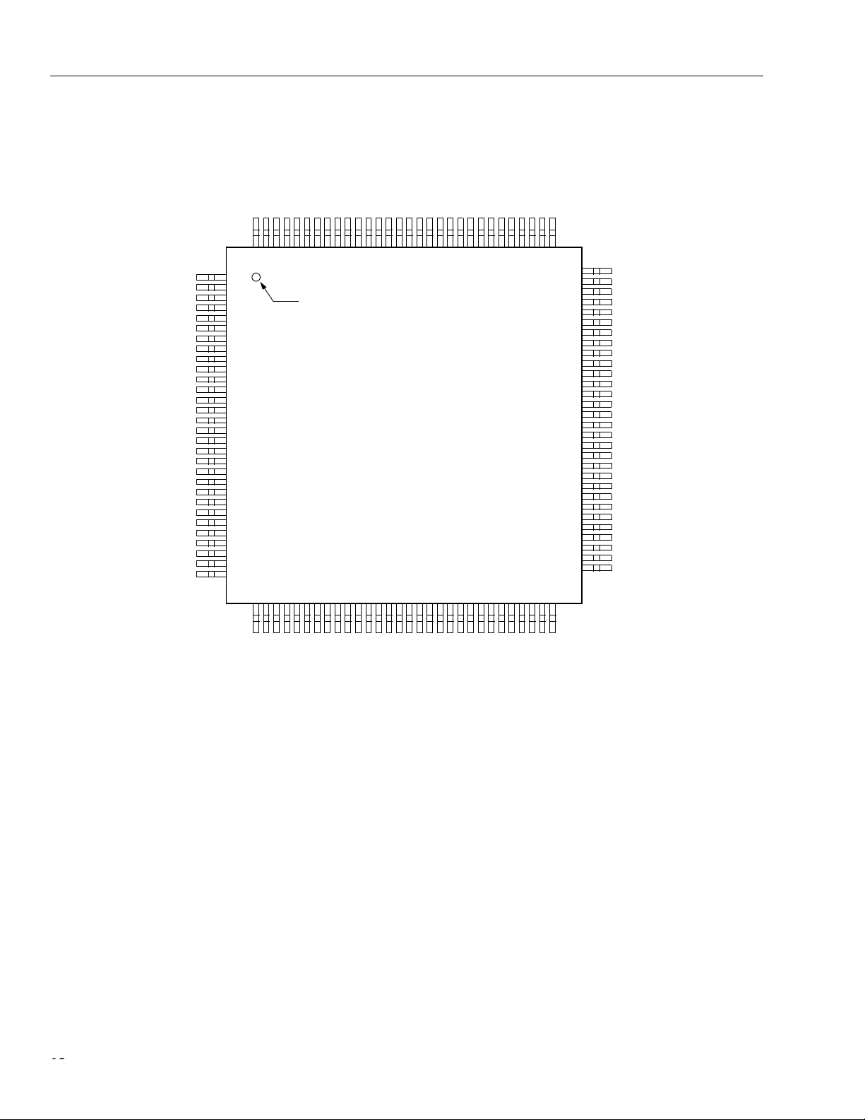
Pin Information
DDA
DDAVSSAVSSA
TPB1–
V
TPA1+
TPA1–
TPB1+
96
97
98
V
91
92
93
94
95
90
89
88
87
86
85
84
83
82
81
80
79
78
77
76
75
74
73
72
71
70
69
68
67
66
65
64
63
62
61
V
SSA
CPS
V
DD
NC
LPS
LKON
PC0
PC1
PC2
CONTENDER
PCI_VIOS
PCI_AD[0]
PCI_AD[1]
V
DD
V
SS
PCI_AD[2]
PCI_AD[3]
PCI_AD[4]
V
SS
PCI_AD[5]
PCI_AD[6]
PCI_AD[7]
PCI_CBEN[0]
V
DD
V
SS
PCI_AD[8]
PCI_AD[9]
PCI_AD[10]
PCI_AD[11]
V
SS
60
CNA
TEST1
ROM_CLK
ROM_AD
TEST0
V
V
CLKRUNN
PCI_INTAN
PCI_RSTN
PCI_GNTN
PCI_REQN
PCI_PMEN
V
PCI_CLK
V
PCI_AD[31]
PCI_AD[30]
PCI_AD[29]
PCI_AD[28]
V
V
PCI_AD[27]
PCI_AD[26]
PCI_AD[25]
PCI_AD[24]
PCI_CBEN[3]
V
PCI_IDSEL
PCI_AD[23]
DDAVSSA
TPA0–
TPB0+
TPB0–
CARDBUSN
VDDNCNCSESMPTEST
118
119
120
1
2
3
4
5
DD
SS
DD
SS
DD
SS
SS
6
7
8
9
10
11
12
13
14
15
16
17
18
19
20
21
22
23
24
25
26
27
28
29
30
31323334353637
RESETNXOXI
111
112
113
114
115
116
117
PIN #1 IDENTIFIER
394041424344454647484950515253545556575859
38
PLLVSSPLLVDDR1R0V
107
108
109
110
TPBIAS0
104
105
106
TPBIAS1
TPA0+
99
103
101
102
100
SS
DD
V
V
PCI_AD[22]
PCI_AD[21]
SS
DD
V
V
PCI_AD[20]
PCI_AD[19]
PCI_AD[18]
PCI_AD[17]
SS
DD
V
V
PCI_AD[16]
PCI_IRDYN
PCI_CBEN[2]
PCI_FRAMEN
PCI_TRDYN
PCI_DEVSELN
SS
DD
V
V
SS
V
PCI_PAR
PCI_STOPN
PCI_PERRN
PCI_SERRN
PCI_CBEN[1]
Note: Active-low signals within this document are indicated by an N following the symbol names.
Figure 3. Pin Assignments for FW322
PCI_AD[15]
PCI_AD[14]
PCI_AD[13]
PCI_AD[12]
1074 (F) R.01
1212 Lucent Technologies Inc.

Data Sheet, Rev. 1 FW322
February 2001 1394A PCI PHY/Link Open Host Controller Interface
Pin Information
(continued)
Table 1. Pin Descriptions
Pin Symbol*
1CNA O
Type Description
Cable Not Active.
legacy power management systems.
2TEST1 I
3 ROM_CLK I/O
4 ROM_AD I/O
5TEST0 I
6V
7V
DD
SS
—
—
8 CLKRUNN I/O
Test.
Used for device testing. Tie to V
ROM Clock.
ROM Address/Data.
Test.
Used for device testing. Tie to V
Power.
Ground.
CLKRUNN (Active-Low).
mobile environment. If not used, CLKRUNN pin needs
to be pulled down to V
9 PCI_INTAN O
10 PCI_RSTN I
11 PCI_GNTN I
12 PCI_REQN O
13 PCI_PMEN O
14 V
DD
—
15 PCI_CLK I
16 V
SS
—
17 PCI_AD[31] I/O
18 PCI_AD[30] I/O
19 PCI_AD[29] I/O
20 PCI_AD[28] I/O
21 V
22 V
DD
SS
—
—
23 PCI_AD[27] I/O
24 PCI_AD[26] I/O
25 PCI_AD[25] I/O
26 PCI_AD[24] I/O
27 V
SS
—
28 PCI_CBEN[3] I/O
29 PCI_IDSEL I
30 PCI_AD[23] I/O
31 PCI_AD[22] I/O
32 V
33 V
DD
SS
—
—
34 PCI_AD[21] I/O
35 PCI_AD[20] I/O
36 PCI_AD[19] I/O
37 PCI_AD[18] I/O
38 V
39 V
DD
SS
—
—
40 PCI_AD[17] I/O
* Active-low signals within this document are indicated by an N following the symbol names.
PCI Interrupt (Active-Low).
PCI Reset (Active-Low).
PCI Grant Signal (Active-Low).
PCI Request Signal (Active-Low).
PCI Power Management Event (Active-Low).
Power.
PCI Clock Input.
Ground.
PCI Address/Data Bit.
PCI Address/Data Bit.
PCI Address/Data Bit.
PCI Address/Data Bit.
Power.
Ground.
PCI Address/Data Bit.
PCI Address/Data Bit.
PCI Address/Data Bit.
PCI Address/Data Bit.
Ground.
PCI Command/Byte Enable (Active-Low).
PCI ID Select.
PCI Address/Data Bit.
PCI Address/Data Bit.
Power.
Ground.
PCI Address/Data Bit.
PCI Address/Data Bit.
PCI Address/Data Bit.
PCI Address/Data Bit.
Power.
Ground.
PCI Address/Data Bit.
CNA output is provided for use in
.
SS
.
SS
Optional signal for PCI
for correct operation.
SS
33 MHz.
Lucent Technologies Inc. 13

FW322 Data Sheet, Rev. 1
1394A PCI PHY/Link Op en Host Controller Interface February 2001
Pin Information
Table 1. Pin Descriptions
Pin Symbol*
41 PCI_AD[16] I/O
42 PCI_CBEN[2] I/O
43 PCI_FRAMEN I/O
44 V
45 V
46 PCI_IRDYN I/O
47 PCI_TRDYN I/O
48 PCI_DEVSELN I/O
49 PCI_STOPN I/O
50 V
51 V
52 PCI_PERRN I/O
53 PCI_SERRN I/O
54 PCI_PAR I/O
55 PCI_CBEN[1] I/O
56 V
57 PCI_AD[15] I/O
58 PCI_AD[14] I/O
59 PCI_AD[13] I/O
60 PCI_AD[12] I/O
61 V
62 PCI_AD[11] I/O
63 PCI_AD[10] I/O
64 PCI_AD[9] I/O
65 PCI_AD[8] I/O
66 V
67 V
68 PCI_CBEN[0] I/O
69 PCI_AD[7] I/O
70 PCI_AD[6] I/O
71 PCI_AD[5] I/O
72 V
73 PCI_AD[4] I/O
74 PCI_AD[3] I/O
75 PCI_AD[2] I/O
76 V
77 V
78 PCI_AD[1] I/O
79 PCI_AD[0] I/O
80 PCI_VIOS —
81 CONTENDER I
(continued)
(continued)
DD
SS
DD
SS
SS
SS
SS
DD
SS
SS
DD
Type Description
PCI Address/Data Bit.
PCI Command/Byte Enable Signal (Active-Low).
PCI Frame Signal (Active-Low).
—
—
Power.
Ground.
PCI Initiator Ready Signal (Active-Low).
PCI Target Ready Signal (Active-Low).
PCI Device Select Signal (Active-Low).
PCI Stop Signal (Active-Low).
—
—
Power.
Ground.
PCI Parity Error Signal (Active-Low).
PCI System Error Signal (Active-Low).
PCI Parity Signal.
PCI Command/Byte Enable Signal (Active-Low).
—
Ground.
PCI Address/Data Bit.
PCI Address/Data Bit.
PCI Address/Data Bit.
PCI Address/Data Bit.
—
Ground.
PCI Address/Data Bit.
PCI Address/Data Bit.
PCI Address/Data Bit.
PCI Address/Data Bit.
—
—
Ground.
Power.
PCI Command/Byte Enable Signal (Active-Low).
PCI Address/Data Bit.
PCI Address/Data Bit.
PCI Address/Data Bit.
—
Ground.
PCI Address/Data Bit.
PCI Address/Data Bit.
PCI Address/Data Bit.
—
—
Ground.
Power.
PCI Address/Data Bit.
PCI Address/Data Bit.
PCI Signaling Indicator.
Contender.
On hardware reset, this input sets the
(5 V or 3.3 V.)
default value of the CONTENDER bit indicated during
self-ID. This bit can be programmed by tying the signal
DD
to V
(high) or to ground (low).
* Active-low signals within this document are indicated by an N following the symbol names.
1414 Lucent Technologies Inc.

Data Sheet, Rev. 1 FW322
February 2001 1394A PCI PHY/Link Open Host Controller Interface
Pin Information
Table 1. Pin Decriptions
Pin Symbol*
82 PC2 I
83 PC1
84 PC0
(continued)
(continued)
Type Description
Power-Class Indicators.
inputs set the default value of the power class indicated
during self-ID. These bits can be programmed by tying
the signals to V
85 LKON O
Link On.
Signal from the internal PHY core to the
internal link core. This signal is provided as an output
for use in legacy power management systems.
86 LPS O
Link Po wer Status.
the internal PHY core. LPS is provided as an output for
use in legacy power management systems.
87 NC —
88 V
DD
—
89 CPS I
No Connect.
Power.
Cable P o wer St atus.
cable power through a 400 kΩ resistor. This circuit
drives an internal comparator that detects the presence
of cable power. This information is maintained in one
internal register and is available to the LLC by way of a
register read (see IEEE 1394a-2000, Standard for a
High Performance Serial Bus (Supplement)).
90 V
SSA
—
Analog Circuit Ground.
tied together to a low-impedance ground plane.
91 V
DDA
—
Analog Circuit Power.
analog portion of the device.
92 V
SSA
—
Analog Circuit Ground.
tied together to a low-impedance ground plane.
93 V
SSA
—
Analog Circuit Ground.
tied together to a low-impedance ground plane.
94 V
DDA
—
Analog Circuit Ground.
analog portion of the device.
95 TPB1– Analog I/O
Port 1, Port Cable Pair B.
tion to the twisted-pair cable. Board traces from each
96 TPB1+
pair of positive and negative differential signal pins
should be kept matched and as short as possible to the
external load resistors and to the cable connector.
97 TPA1– Analog I/O
Port 1, Port Cable Pair A.
tion to the twisted-pair cable. Board traces from each
98 TPA1+
pair of positive and negative differential signal pins
should be kept matched and as short as possible to the
external load resistors and to the cable connector.
99 TPBIAS1 Analog I/O
Port 1, Twisted-Pair Bias.
1.86 V nominal bias voltage needed for proper operation of the twisted-pair cable drivers and receivers and
for sending a valid cable connection signal to the
remote nodes.
* Active-low signals within this document are indicated by an N following the symbol names.
On hardware reset, these
(high) or to ground (low).
DD
Signal fro m the i nternal li nk co re to
CPS is normally connected to the
All V
V
DDA
All V
All V
V
signals should be
SSA
supplies power to the
signals should be
SSA
signals should be
SSA
supplies power to the
DDA
TPB1± is the port B connec-
TPA1± is the port A connec-
TPBIAS1 provides the
Lucent Technologies Inc. 15

FW322 Data Sheet, Rev. 1
1394A PCI PHY/Link Op en Host Controller Interface February 2001
Pin Information
Table 1. Pin Descriptions
Pin Symbol*
100 TPB0– Analog I/O
(continued)
(continued)
Type Description
Port 0, Port Cable Pair B.
tion to the twisted-pair cable. Board traces from each
101 TPB0+
pair of positive and negative differential signal pins
should be kept matched and as short as possible to the
external load resistors and to the cable connector.
102 TPA0– Analog I/O
Port 0, Port Cable Pair A.
tion to the twisted-pair cable. Board traces from each
103 TPA0+
pair of positive and negative differential signal pins
should be kept matched and as short as possible to the
external load resistors and to the cable connector.
104 TPBIAS0 Analog I/O
Port 0, Twisted-Pair Bias.
1.86 V nominal bias voltage needed for proper operation of the twisted-pair cable drivers and receivers and
for sending a valid cable connection signal to the
remote nodes.
105 V
SSA
—
Analog Circuit Ground.
tied together to a low-impedance ground plane.
106 V
DDA
—
Analog Circuit Power.
analog portion of the device.
107 R0 I
Current Setting Resistor.
voltage is applied to a resistor connected between R0
and R1 to set the operating current and the cable driver
108 R1
output current. A low temperature-coefficient resistor
(TCR) with a value of 2.49 kΩ ± 1% should be used to
meet the IEEE 1394-1995 standard requirements for
output voltage limits.
109 PLLV
DD
—
Power for PLL Circuit.
PLL circuitry portion of the device.
110 PLLV
SS
—
Ground for PLL Cir cuit.
ance ground plane.
111 XI —
Crystal Oscillator.
24.576 MHz parallel resonant fundamental mode
crystal. Although when a 24.576 MHz clock source is
used, it can be connected to XI with XO left uncon-
112 XO
nected. The optimum values for the external shunt
capacitors are dependent on the specifications of the
crystal used. The suggested values of 12 pF are appropriate for crystal with 7 pF specified loads. For more
details, see the Crystal Selection Considerations
section.
* Active-low signals within this document are indicated by an N following the symbol names.
TPB0± is the port B connec-
TPA0± is the port A connec-
TPBIAS0 provides the
All V
V
DDA
signals should be
SSA
supplies power to the
An internal reference
PLLV
supplies power to the
DD
PLLVSS is tied to a low-imped-
XI and XO connect to a
1616 Lucent Technologies Inc.

Data Sheet, Rev. 1 FW322
February 2001 1394A PCI PHY/Link Open Host Controller Interface
Pin Information
Table 1. Pin Descriptions
Pin Symbol*
113 RESETN I
(continued)
(continued)
Type Description
Reset (Ac tive-Low).
(active), a bus reset condition is set on the active cable
ports and the internal PHY core logic is reset to the
reset start state. An internal pull-up resistor, which is
connected to V
capacitor and resistor are required. This input is a standard logic buffer and can also be driven by an opendrain logic output buffer.
114 PTEST I
115 SM I
Test.
Used for device testing. Tie to V
Test Mode Control.
turing test and should be tied to V
116 SE I
Test Mode Control.
turing test and should be tied to V
117 NC —
118 NC —
119 V
DD
—
120 CARDBUSN I
No Connect.
No Connect.
Power.
CardBusN.
Selects mode of operation for PCI output
buffers. Tie low for cardbus operation, high for PCI
operation. An internal pull-up is provided to force
buffers to PCI mode, if no connection is made to this
pin.
* Active-low signals within this document are indicated by an N following the symbol names.
When RESETN is asserted low
, is provided, so only an external delay
DD
.
SS
SM is used during the manufac-
.
SS
SE is used during the manufac-
.
SS
Application Schematic
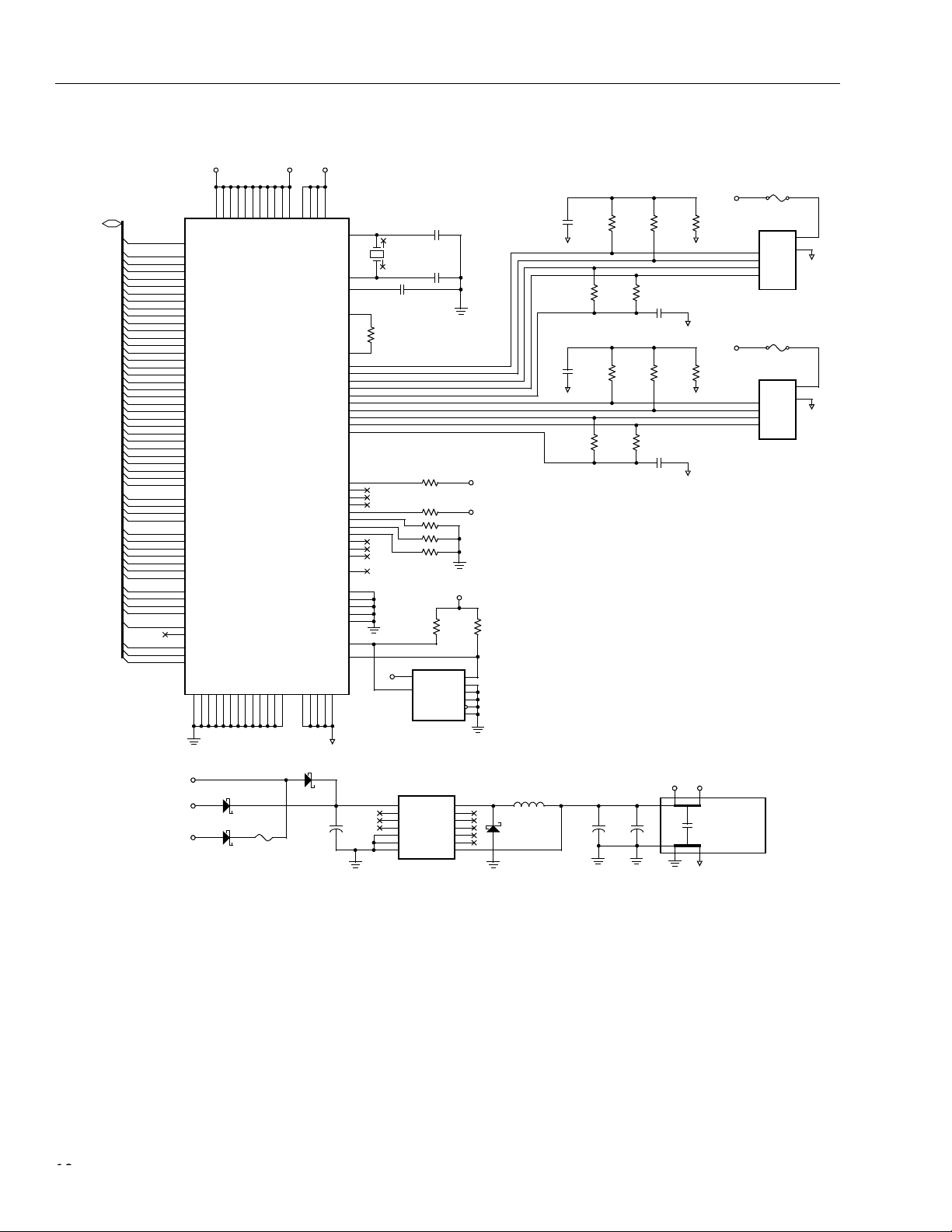
The application schematic presents a complete two-port, 400 Mbits/s IEEE 1394a-2000 design, featuring the
Lucent FW322 PCI bus-based host OHCI controller and 400 Mbits/s PHY core. The FW322 device needs only a
power source (U3), connection to PCI interface, 1394a-2000 terminators and connectors, crystal, and serial
EEPROM. No external PHY is required because the FW322 contains both host controller and PHY core functions.
This design is a secondary (Class 4) power provider to the 1394 bus, and will participate in the required 1394a2000 bus activities, even when power on the PCI bus is not energized.
Lucent Technologies Inc. 17
FW322 Data Sheet, Rev. 1
1394A PCI PHY/Link Op en Host Controller Interface February 2001
Application Schematic
+3.3 V +3.3 V +3.3 VA
11988776750443832211469194
AD0
AD1
AD2
AD3
AD4
AD5
AD6
AD7
AD8
AD9
AD10
AD11
AD12
AD13
AD14
AD15
AD16
AD17
AD18
AD19
AD20
AD21
AD22
AD23
AD24
AD25
AD26
AD27
AD28
AD29
AD30
AD31
PAR
IRDY#
TRDY#
STOP#
IDSEL
REQ#
GNT#
CLK
RST#
INTA#
PME#
BPWR
+5 V PCI
+12 V PCI
80
79
78
75
74
73
71
70
69
65
64
63
62
60
59
58
57
41
40
37
36
35
34
31
30
26
25
24
23
20
19
18
17
55
42
28
54
43
46
47
48
49
29
12
11
52
53
15
8
10
9
13
U1
VDD
VDD
VDD
PCI_VIOS
PCI_AD0
PCI_AD1
PCI_AD2
PCI_AD3
PCI_AD4
PCI_AD5
PCI_AD6
PCI_AD7
PCI_AD8
PCI_AD9
PCI_AD10
PCI_AD11
PCI_AD12
PCI_AD13
PCI_AD14
PCI_AD15
PCI_AD16
PCI_AD17
PCI_AD18
PCI_AD19
PCI_AD20
PCI_AD21
PCI_AD22
PCI_AD23
PCI_AD24
PCI_AD25
PCI_AD26
PCI_AD27
PCI_AD28
PCI_AD29
PCI_AD30
PCI_AD31
PCI_CBEN0
PCI_CBEN1
PCI_CBEN2
PCI_CBEN3
PCI_PAR
PCI_FRAMEN
PCI_IRDYN
PCI_TRDYN
PCI_DEVSELN
PCI_STOPN
PCI_IDSEL
PCI_REQN
PCI_GNTN
PCI_PERRN
PCI_SERRN
PCI_CLK
PCI_CLKRUNN
PCI_RSTN
PCI_INTAN
PCI_PMEN
7
VDD
VSS
VSS
VSS
VSS
VSS
VSS
VSS
1622273339455156616672
CR2
MBRS340T3
CR4
MBRS340T3
1.5 A RESETTABLE
VDD
VSS
VDD
FW322
VSS
F4
PCI BUS
C_BE#0 68
C_BE#1
C_BE#2
C_BE#3
FRAME#
DEVSEL#
PERR#
SERR#
(continued)
106
VDD
VDD
VDD
VDD
VDD
VDDA
VDDA
VDDA
RESETN
TPBIAS0
TPBIAS1
CONTENDER
CARDBUSN
ROM_AD
ROM_CLK
VSS
VSS
VSS
VSS
PLLVSS
VSSA
VSSA
76
939290
110
105
CR1
MBRS340T3
C12
22
µ
50 V
109
111
XI
4
PLLVDD
1
112
XO
113
108
R1
R7
2.49 k
1/10 W
107
R0
100
TPB0–
101
TPB0+
102
TPA0–
103
TPA0+
104
95
TPB1–
96
TPB1+
97
TPA1–
98
TPA1+
99
89
CPS
87
NC
86
LPS
85
LKON
84
PC0
83
PC1
82
PC2
81
117
NC
118
NC
120
1
CNA
5
TEST0
2
TEST1
114
PTEST
116
SE
115
SM
4
3
VSSA
VSSA
AGND
U3 SUPPLIES VDDX POWER; IT IS SOURCE D
BY THE MOST POSITIVE OF PCI +5 V, PCI +12 V,
AND 1394 BUS POWER (BPWR).
PWRSRC 10
+
F
Y1
3
24.576 M H z
2
C5
0.1 µF
Ω
ROM_AD
ROM_CLK
+3.3 V
1
2
7
5
4
6
12 pF
12 pF
1%
R13 402 kΩ 1%
R14 10 k
R18 10 k
R19 10 k
R20 10 k
8
VCC
5
SDATA
AT24C02AN-2.7
U3
VIN
NC
NC
NC
ON/OFF
SIGGND
PWRGND
LM2574HVM -3. 3
C3
C4
U2
VOUT
Ω
Ω
Ω
Ω
10 k
SCLK
NC
NC
NC
NC
NC
FB
GND
+3.3 V
Ω
A0
A1
A2
WP
F1
OMNI-BLOCK FUSE
BPWR
BPWR
1394A PORT 1
J1
VP
3
VG
TPB–
4
TPB+
5
TPA–
6
TPA+
F2
OMNI-BLOCK FUSE
1394A PORT 2
J2
VP
VG
3
TPB–
4
TPB+
5
TPA–
6
TPA+
1
2
AGND
1
2
AGND
R2
1%
R9
1%
0.33
0.33
4.99
C6
µ
4.99
C8
µ
R3
1%
Ω
1/10 W
AGND
F
AGND
R10
1%
Ω
1/10 W
AGND
F
AGND
+3.3 V +3.3 VA
AGND
POWER PLANE
FILTERING
GROUND PLANE
R1
C1
1%
56.2
56.2
Ω
220 pF
1/10 W
AGND
R4
1%
56.2
Ω
1/10 W
C7
56.2
220 pF
1/10 W
AGND
R11
56.2
1%
Ω
1/10 W
BPWR
+3.3 V
R24R23
10 k
Ω
6
1
2
EEPROM
3
7
4
L1
H
680
12
8
9
11
13
14
3
µ
CR3
MBRS1100T3
100
10 V
C13
F
µ
Ω
1/10 W
R5
56.2 Ω 1%
1/10 W
R8
56.2
1%
Ω
Ω
1/10 W
R12
56.2 Ω 1%
1/10 W
++
C14
100 µF
10 V
5-8886 (F)a
Figure 4. Application Schematic for FW322
1818 Lucent Technologies Inc.

Data Sheet, Rev. 1 FW322
February 2001 1394A PCI PHY/Link Open Host Controller Interface
Internal Registers
This section describes the internal registers in FW322, including both PCI configuration registers and OHCI registers. All registers are detailed in the same format; a brief description for each register, followed by the register offset
and a bit table describing the reset state for each register.
A bit description table indicates bit-field names, a detailed field description, and field access tags.
Table 2 describes the field access tags.
Table 2. Bit-Field Access T a g Description
Access Tag Name Description
R Read Field may be read by software.
W Write Field may be written by software to any value.
S Set Field may be set by a write of 1. Writes of 0 have no effect.
C Clear Field may be cleared by a write of 1. Writes of 0 have no effect.
U Update Field may be autonomously updated by the FW322.
PCI Configuration Registers
Table 3 illustrates the PCI configuration header that includes both the predefined portion of the configuration
space and the user-definable registers.
Table 3. PCI Configuration Register Map
Register Name Offset
Device ID Vendor ID 00h
Status Command 04h
Class Code Revision ID 08h
BIST He ade r Type Laten cy Timer Cache Line Size 0Ch
OHCI Registers Base Address 10h
Reserved 14h
Reserved 18h
Reserved 1Ch
Reserved 20h
Reserved 24h
Reserved 28h
Subsystem ID Subsystem Vendor ID 2Ch
Reserved 30h
Reserved Capabilities Pointer 34h
Reserved 38h
Maximum Latency Minimum Grant Interrupt Pin Interrupt Line 3Ch
PCI OHCI Control Register 40h
Power Management Capabilities Next Item Pointer Capability ID 44h
Pm Data Pmcsr_bse Power Management CSR 48h
Reserved 4C—FCh
Lucent Technologies Inc. 19

FW322 Data Sheet, Rev. 1
1394A PCI PHY/Link Op en Host Controller Interface February 2001
Internal Registers
(continued)
Vendor ID Register
The vendor ID register contains a value allocated by the PCI SIG and identifies the manufacturer of the device.
The vendor ID assigned to Lucent Technologies is 11C1h.
Table 4. Vendor ID Register
Bit
15 Vendor ID R 0
14 R 0
13 R 0
12 R 1
11 R 0
10 R 0
9R0
8R1
7R1
6R1
5R0
4R0
3R0
2R0
1R0
0R1
Field
Name
Type Default
Register: Vendor ID register
Type: Read only
Offset: 00h
Default: 11C1h
2020 Lucent Technologies Inc.

Data Sheet, Rev. 1 FW322
February 2001 1394A PCI PHY/Link Open Host Controller Interface
Internal Registers
(continued)
Device ID Regist er
The device ID register contains a value assigned to the FW322 by Lucent Technologies. The device identification
for the FW322 is 5811h.
Table 5. Device ID Register
Bit
15 Device ID R 0
14 R 1
13 R 0
12 R 1
11 R 1
10 R 0
9R0
8R0
7R0
6R0
5R0
4R1
3R0
2R0
1R0
0R1
Field
Name
Type Default
Register: Device ID register
Type: Read only
Offset: 02h
Default: 5811h
Lucent Technologies Inc. 21

FW322 Data Sheet, Rev. 1
1394A PCI PHY/Link Op en Host Controller Interface February 2001
Internal Registers
(continued)
PCI Command Register
The command register provides control over the FW322 interface to the PCI bus. All bit functions adhere to the
definitions in the PCI local bus specification, as in the following bit descriptions.
Table 6. PCI Command Register
Bit
15 Reserved R 0
14 R 0
13 R 0
12 R 0
11 R 0
10 R 0
9FBB_ENB R 0
8SERR_ENBRW 0
7STEP_ENB R 0
6PERR_ENBRW 0
5VGA_ENB R 0
4MWI_ENBRW0
3SPECIAL R 0
2MASTER_ENBRW 0
1 MEMORY_ENB RW 0
0IO_ENB R0
Field
Name
Type Default
Register: PCI command register
Type: Read/Write
Offset: 04h
Default: 0000h
2222 Lucent Technologies Inc.

Data Sheet, Rev. 1 FW322
February 2001 1394A PCI PHY/Link Open Host Controller Interface
Internal Registers
Table 7. PCI Command Register Description
Bit Field Name Type Description
15:10 Reserved R
9FBB_ENBR
8 SERR_ENB RW
7 STEP_ENB R
6 PERR_ENB RW
5VGA_ENBR
4MWI_ENBRW
3SPECIALR
2 MASTER_ENB RW
1 MEMORY_ENB RW
0IO_ENBR
(continued)
Reserved.
Fast Back-to-Bac k Enable.
back transactions; thus, this bit returns 0 when read.
SERR Enable.
SERR can be asserted after detecting an address parity error on the PCI
bus.
Address/Data Stepping Control.
address/data stepping; thus, this bit is hardwired to 0.
Parity Er ror Enable.
PERR response to parity errors through the PERR signal.
VGA Palette Snoop Enable.
snooping. This bit returns 0 when read.
Memory Write and Invalidate Enable.
is enabled to generate MWI PCI bus commands. If this bit is reset, then
the FW322 generates memory write commands instead.
Special Cycle Enable.
cycle transactions. This bit returns 0 when read.
Bus Master Enable.
initiate cycles on the PCI bus.
Memory Response Enable.
respond to memory cycles on the PCI bus. This bit must be set to access
OHCI registers.
I/O Space Enable.
functionality; thus, this bit returns 0 when read.
Bits 15:10 return 0s when read.
The FW322 does not generate fast back-to-
When this bit is set, the FW322 SERR driver is enabled.
When this bit is set, the FW322 is enabled to drive
The FW322 does not feature VGA palette
The FW322 function does not respond to special
When this bit is set, the FW322 is enabled to
Setting this bit enables the FW322 to
The FW322 does not implement any I/O mapped
The FW322 does not support
When this bit is set, the FW322
Lucent Technologies Inc. 23

FW322 Data Sheet, Rev. 1
1394A PCI PHY/Link Op en Host Controller Interface February 2001
Internal Registers
(continued)
PCI Status Register
The status register provides status over the FW322 interface to the PCI bus. All bit functions adhere to the
definitions in the PCI local bus specification, as in the following bit descriptions.
Table 8. PCI Status Register
Bit
15 PAR_ERR RCU 0
14 SYS_ERR RCU 0
13 MABORT RCU 0
12 TABORT_REC RCU 0
11 TABORT_SIG RCU 0
10 PCI_SPEED R 0
9R1
8 DATAPAR RCU 0
7FBB_CAP R 0
6 UDF R 0
5 66MHZ R 0
4CAPLIST R 1
3 Reserved R 0
2R0
1R0
0R0
Field
Name
Type Default
Register: PCI status register
Type: Read/Clear/Update
Offset: 06h
Default: 0210h
2424 Lucent Technologies Inc.

Data Sheet, Rev. 1 FW322
February 2001 1394A PCI PHY/Link Open Host Controller Interface
Internal Registers
(continued)
Class Code and Revision ID Register
The class code register and revision ID register categorizes the FW322 as a serial bus controller (0Ch),
controlling an IEEE 1394 bus (00h), with an OHCI programming model (10h). Furthermore, the chip revision is
indicated in the lower byte.
Table 9. Class Code and Revision ID Register
Bit
31 BASECLASS R 0
30 R 0
29 R 0
28 R 0
27 R 1
26 R 1
25 R 0
24 R 0
23 SUBCLASS R 0
22 R 0
21 R 0
20 R 0
19 R 0
18 R 0
17 R 0
16 R 0
15 PGMIF R 0
14 R 0
13 R 0
12 R 1
11 R 0
10 R 0
9R0
8R0
7 CHIPREV R 0
6R0
5R0
4R0
3R0
2R0
1R0
0R0
Field
Name
Type Default
Register: Class code and revision ID register
Type: Read only
Offset: 08h
Default: 0C00 1000h
Lucent Technologies Inc. 25

FW322 Data Sheet, Rev. 1
1394A PCI PHY/Link Op en Host Controller Interface February 2001
Internal Registers
Table 10. Class Code and Revision ID Register Description
Bit Field Name Type Description
31:24 BASECLASS R
23:16 SUBCLASS R
15:8 PGMIF R
7:0 CHIPREV R
(continued )
Base Class.
tion as a serial bus controller.
Subclass.
the function as an IEEE 1394 serial bus controller.
Programming Interface.
that the programming model is compliant with the 1394 Open Host
Controller Interface Specification.
Silicon Revision.
revision of the FW322.
This field returns 0Ch when read, which classifies the func-
This field returns 00h when read, which specifically classifies
This field returns 10h when read, indicating
This field returns 04h when read, indicating the silicon
Latency Ti mer and Class Cache Line Size Register
The latency timer and class cache line size register is programmed by host BIOS to indicate system cache line
size and the latency timer associated with the FW322.
Table 11. Latency Timer and Class Cache Line Size Register
Bit
15 LATENCY_TIMER RW 0
14 RW 0
13 RW 0
12 RW 0
11 RW 0
10 RW 0
9RW0
8RW0
7 CACHELINE_SZ RW 0
6RW0
5RW0
4RW0
3RW0
2RW0
1RW0
0RW0
Field
Name
Type Default
Register: Latency timer and class cache line size register
Type: Read/Write
Offset: 0Ch
Default: 0000h
2626 Lucent Technologies Inc.

Data Sheet, Rev. 1 FW322
February 2001 1394A PCI PHY/Link Open Host Controller Interface
Internal Registers
Table 12. Latency Timer and Class Cache Line Size Register Description
Bit Field Name Type Description
15:8 LATENCY_TIMER RW
7:0 CACHELINE_SZ RW
(continued)
PCI Latency Timer.
timer for the FW322, in units of PCI clock cycles. When the FW322 is
a PCI bus initiator and asserts FRAME, the latency timer begins
counting from zero. If the latency timer expires before the FW322
transaction has terminated, then the FW322 terminates the transaction when its GNT is deasserted.
Cache Line Size.
write and invalidate, memory read line, and memory read multiple
transactions.
The value in this register specifies the latency
This value is used by the FW322 during memory
Header Type and BIST Register
The header type and BIST register indicates the FW322 PCI header type and indicates no built-in self-test.
Table 13. Header Type and BIST Register
Bit
15 BIST R 0
14 R 0
13 R 0
12 R 0
11 R 0
10 R 0
9R0
8R0
7 HEADER_TYPE R 0
6R0
5R0
4R0
3R0
2R0
1R0
0R0
Field
Name
Type Default
Register: Header type and BIST register
Type: Read only
Offset: 0Eh
Default: 0000h
Lucent Technologies Inc. 27

FW322 Data Sheet, Rev. 1
1394A PCI PHY/Link Op en Host Controller Interface February 2001
Internal Registers
Table 14. Header Type and BIST Register Description
Bit Field Name Type Description
15:8 BIST R
7:0 HEADER_TYPE R
(continued)
Built-In Self-Test.
thus, this field returns 00h when read.
PCI Header Type.
this is communicated by returning 00h when this field is read.
The FW322 does not include a built-in self-test;
The FW322 includes the standard PCI header, and
2828 Lucent Technologies Inc.

Data Sheet, Rev. 1 FW322
February 2001 1394A PCI PHY/Link Open Host Controller Interface
Internal Registers
(continued)
OHCI Base Address Register
The OHCI base address register is programmed with a base address referencing the memory-mapped OHCI control. When BIOS writes all 1s to this register, the value read back is FFFF F000h, indicating that 4 Kbytes of memory address space are required for the OHCI registers.
Table 15. OHCI Base Address Register
Field
Bit
Name
31 RW OHCIREG_PTR 0
30 RW 0
29 RW 0
28 RW 0
27 RW 0
26 RW 0
25 RW 0
24 RW 0
23 RW 0
22 RW 0
21 RW 0
20 RW 0
19 RW 0
18 RW 0
17 RW 0
16 RW 0
15 RW 0
14 RW 0
13 RW 0
12 RW 0
11 RW OHCI_SZ 0
10 R 0
9R 0
8R 0
7R 0
6R 0
5R 0
4R 0
3 R OHCI_PF 0
2 R OHCI_MEMTYPE 0
1R 0
0 R OHCI_MEM 0
Type Default
Register: OHCI base address register
Type: Read/Write
Offset: 10h
Default: 0000 0000h
Lucent Technologies Inc. 29

FW322 Data Sheet, Rev. 1
1394A PCI PHY/Link Op en Host Controller Interface February 2001
Internal Registers
Table 16. OHCI Base Address Register Description
Bit Field Name T ype Description
31:12 OHCIREG_PTR RW
11:4 OHCI_SZ R
3 OHCI_PF R
2:1 OHCI_MEMTYPE R
0 OHCI_MEM R
(continued)
OHCI Regi ster P oin ter.
base address register.
OHCI Register Size.
the OHCI registers require a 4 Kbyte region of memory.
OHCI Register Prefetch.
the OHCI registers are nonprefetchable.
OHCI Memory Type.
the OHCI base address register is 32 bits wide and mapping can be
done anywhere in the 32-bit memory space.
OHCI Memory Indicator
the OHCI registers are mapped into system memory space.
Specifies the upper 20 bits of the 32-bit OHCI
This field returns 0s when read, indicating that
This bit returns 0 when read, indicating that
This field returns 0s when read, indicating that
. This bit returns 0 when read, indicating that
3030 Lucent Technologies Inc.
 Loading...