

AGERE DSP1628 Datasheet
Advisory
May 1999
Clarification to the Serial I/O Control Register
Description for the DSP1620/27/28/29 Devices
Active Clock Frequency
The purpose of this advisory is to clarify the function of the serial I/O control registers in the DSP1620/27/28/29
devices. Specifically, it clarifies the function of the control register field that specifies the active clock frequency .
The device data sheets state that the active clock frequency is a ratio of the
pin (DSP1627/28/29 devices) or the output clock frequency on the CKO pin (DSP1620 device). For all four
devices, the actual active clock frequency is a ratio of the
as either the input clock frequency on the CKI pin or the output of an internal clock synthesizer (PLL).
Table 1 summarizes information for each of the four devices. It lists the document number for each device data
sheet. For example, the data sheet for the DSP1620, entitled
ment number DS97-321WDSP. Table 1 also lists the name of each serial I/O unit on each device, the corresponding control register, the data sheet page number that describes the register, and the corresponding field
within the register that specifies the active clock frequency. For e xample, the DSP1620 contains two serial I/O
units named SIO and SSIO. The control register for SIO is
Bits 8—7 within
sioc
(CLK1 field) specify the active clock frequency of the SIO.
internal
clock frequency, which can be programmed
DSP1620 Digital Signal Processor
sioc
described on page 94 of the data sheet.
input
clock frequency on the CKI
, has the docu-
Table 1. Data Sheet and Serial I/O Information for the DSP1620/27/28/29 Devices
Device Data Sheet
Document Number
DSP1620 DS97-321WDSP SIO
DSP1627 DS96-188WDSP SIO
DSP1628 DS97-040WDSP SIO
DSP1629 DS96-039WDSP SIO
Table 2 shows a corrected description of the CLK/CLK1/CLK2 field of the serial I/O control register. The
specific correction is shown in bold type—the active clock frequency is a ratio of f
Table 2. Corrected Description of CLK/CLK1/CLK2 Field
Field Value Description
CLK
CLK1
CLK2
Active clock frequency =
00
01
Active clock frequency =
10
Active clock frequency =
11
Active clock frequency =
Name Control
Register
sioc
SSIO
SIO2
SIO2
SIO2
SSIOC
sioc
sioc
sioc
f
internal clock
f
internal clock
f
internal clock
f
internal clock
Serial I/O Units
Data Sheet
Page No.
94 8—7 CLK1
96 8—7 CLK2
45 8—7 CLK
55 8—7 CLK
46 8—7 CLK
÷ 2
÷ 6
÷ 8
÷ 10
Active Clock Frequency
Control Field
Bits Name
internal clock
, not of CKI or CKO.
DRAFT COPY

For additional information, contact your Microelectronics Group Account Manager or the following:
INTERNET:
E-MAIL:
N. AMERICA: Microelectronics Group, Lucent Tech nologies Inc., 555 Union Boulevard, Room 30L-15P-BA, Allentown, PA 1 81 03
ASIA PACIFIC: Microelectronics Group, Lucent Technologies Singap ore Pte. Ltd., 77 Science Park Drive, #03-18 Cintech III, Singapore 118256
CHINA: Microelectr on ic s G r ou p, Lucent Technologies (China) Co., Ltd., A-F2, 23/F, Zao Fong Uni verse Buildin g, 1800 Zhong Shan Xi Ro ad, Shanghai
JAPAN: Microelectronics Group, Lucent Technologies Japan Ltd., 7-18, Higashi-Gotanda 2-chome, Shinagawa-ku, Tokyo 141, Japan
EUROPE: Data Requests: MICROELECTRONICS GROUP DATALINE:
Lucent Technologies Inc. reserves the right to make changes to the product(s) or information contained herein without notice. No liability is assumed as a result of their use or application. No
rights under any patent accompany the sale of any such product(s) or information.
http://www.lucent.com/micro
docmaster@micro.lucent.com
1-800-372-2447
Tel. (65) 778 8833
200233 P. R. China
Tel. (81) 3 5421 1600
Techni cal Inquiries: GERMANY:
, FAX 610-712-4106 (In CANADA:
, FAX (65) 777 7495
Tel . ( 86) 21 6440 0468, ext. 316
, FAX (81) 3 5421 1700
FRANCE:
(39) 02 6608131
ITAL Y:
(49) 89 95086 0
(33) 1 40 83 68 00
(Milan), SPAIN:
1-800-553-2448
, F A X ( 86) 21 6440 0652
(Munich), UNITED KINGDOM:
(Paris), SWEDEN:
, FAX 610-712-4106)
Tel. (44) 1189 324 299
(46) 8 594 607 00
(34) 1 807 1441
(Madrid)
, FAX (44) 1189 328 148
(44) 1344 865 900
(Stockholm), FINLAND:
(Ascot),
(358) 9 4354 2800
(Helsinki),
Copyright © 1999 Lucent Technologies Inc.
All Rights Reserved
May 1999
AY99-001WDSP
(must accompany DS97-321WDSP, DS96-188WDSP, DS97-040WDSP, and DS96-039WDSP)

Preliminary Data Sheet
February 1997
DSP1628 Digital Signal Processor
1 Features
■
Optimized for digital cellular applications with a bit
manipulation unit for higher coding efficiency and
an error correction coprocessor for equalization
and channel coding support.
■
On-chip, programmable, PLL clock synthesizer.
■
19.2 ns and 12.5 ns instruction cycle times at
2.7 V.
■
Mask-programmable memory map option: The
DSP1628x16 features 16 Kwords on-chip dualport RAM. The DSP1628x08 features 8 Kwords
on-chip dual-port RAM. Both feature 48 Kwords
on-chip ROM with a secure option.
■
Low power consumption:
— <1.9 mW/MIPS typical at 2.7 V.
■
Flexible power management modes:
—Standard sleep: 0.2 mW/MIPS at 2.7 V.
—Sleep with slow internal clock: 0.7 mW at 2.7 V.
—Hardware STOP (pin halts DSP): <20 µA.
■
Mask-programmable clock options: small signal,
and CMOS.
■
144 PBGA package (13 mm x 13 mm) available.
■
Sequenced accesses to X and Y external
memory.
■
Object code compatible with the DSP1618.
■
Single-cycle squaring.
■
16 x 16-bit multiplication and 36-bit accumulation
in one instruction cycle.
■
Instruction cache for high-speed, programefficient, zero-overhead looping.
■
Dual 25 Mbit/s serial I/O ports with multiprocessor
capability—16-bit data channel, 8-bit protocol
channel.
■
8-bit parallel host interface
— Supports 8- or 16-bit transfers.
—
Motorola
■
8-bit control I/O interface.
■
256 memory-mapped I/O ports.
■
■
‡
IEEE
Full-speed in-circuit emulation hardware development system on-chip.
Supported by DSP1628 software and hardware
■
development tools.
*
or
Intel
†
compatible.
P1149.1 test port (JTAG boundary scan).
2 Description
The DSP1628 digital signal processor offers 80 MIPS
and 52 MIPS operation at 2.7 V. Designed specifically
for applications requiring low power dissipation in digital cellular systems, the DSP1628 is a signal-coding
device that can be programmed to perform a wide
variety of fixed-point signal processing functions. The
device is based on the DSP1600 core with a bit
manipulation unit for enhanced signal coding efficiency, an external memory sequencer, an error correction coprocessor (ECCP) for more efficient Viterbi
decoding, and an 8-bit parallel host interface for hardware flexibility. The DSP1628 includes a mix of
peripherals specifically intended to support processing-intensive but cost-sensitive applications in the
area of digital wireless communications.
The DSP1628x16 contains 16 Kwords of internal
dual-port RAM (DPRAM), which allows simultaneous
access to two RAM locations in a single instruction cycle. The DSP1628x08 supports the use of 8 Kwords
of DPRAM. Both devices contain 48 Kwords of internal ROM (IROM).
The DSP1628 is object code compatible with the
DSP1618, while providing more memory. The
DSP1628 is pin compatible with the DSP1627. Note
that TRST (JTAG test reset), replaces a VDD pin.
The DSP1628 supports 2.7 V operation with flexible
power management modes required for portable cellular terminals. Several control mechanisms achieve
low-power operation, including a STOP pin for placing
the DSP into a fully static, halted state and a programmable power control register used to power down unused on-chip I/O units. These power management
modes allow for trade-offs between power reduction
and wake-up latency requirements. During system
standby, power consumption is reduced to less than
20 µA.
The on-chip clock synthesizer can be driven by an
external clock whose frequency is a fraction of the
instruction rate.
The device is packaged in a 144-pin PBGA, a 100-pin
BQFP, or a 100-pin TQFP and is available with
19.2 ns and 12.5 ns instruction cycle times at 2.7 V.
*
Motorola
†
‡
is a registered trademark of Motorola, Inc.
Intel
is a registered trademark of Intel Corporation.
IEEE
is a registered trademark of The Institute of Electrical
and Electronics Engineers, Inc.

Preliminary Data Sheet
DSP1628 Digital Signal Processor February 1997
Table of Contents
Contents Page
1 Features...................................................................1
2 Description ...............................................................1
3 Pin Information.........................................................3
4 Hardware Architecture..............................................8
4.1 DSP1628 Architectural Overview.......................8
4.2 DSP1600 Core Architectural Overview............12
4.3 Interrupts and Trap...........................................13
4.4 Memory Maps and Wait-States........................18
4.5 External Memory Interface (EMI).....................21
4.6 Bit Manipulation Unit (BMU).............................22
4.7 Serial I/O Units (SIOs)......................................22
4.8 Parallel Host Interface (PHIF)..........................24
4.9 Bit Input/Output Unit (BIO)...............................25
4.10 Timer..............................................................26
4.11 Error Correction Coprocessor (ECCP)...........26
4.12 JTAG Test Port ..............................................34
4.13 Clock Synthesis..............................................36
4.14 Power Management.......................................39
5 Software Architecture.............................................46
5.1 Instruction Set..................................................46
5.2 Register Settings..............................................55
5.3 Instruction Set Formats....................................66
6 Signal Descriptions.................................................72
6.1 System Interface..............................................72
6.2 External Memory Interface...............................74
6.3 Serial Interface #1............................................75
6.4 Parallel Host Interface or Serial
Interface #2 and Control I/O Interface..............76
6.5 Control I/O Interface.........................................76
6.6 JTAG Test Interface.........................................77
7 Mask-Programmable Options.................................78
7.1 Input Clock Options..........................................78
7.2 Memory Map Options.......................................78
7.3 ROM Security Options .....................................78
8 Device Characteristics............................................79
8.1 Absolute Maximum Ratings .............................79
8.2 Handling Precautions.......................................79
8.3 Recommended Operating Conditions..............79
8.4 Package Thermal Considerations....................80
9 Electrical Characteristics and Requirements..........81
9.1 Power Dissipation ............................................84
Contents Page
10 Timing Characteristics for 2.7 V Operation...........86
10.1 DSP Clock Generation...................................87
10.2 Reset Circuit...................................................88
10.3 Reset Synchronization ...................................89
10.4 JTAG I/O Specifications.................................90
10.5 Interrupt..........................................................91
10.6 Bit Input/Output (BIO).....................................92
10.7 External Memory Interface.............................93
10.8 PHIF Specifications........................................97
10.9 Serial I/O Specifications...............................103
10.10 Multiprocessor Communication..................108
11 Outline Diagrams................................................109
11.1 100-Pin BQFP (Bumpered Quad
Flat Pack) ....................................................109
11.2 100-Pin TQFP (Thin Quad Flat Pack)..........110
11.3 144-Pin PBGA (Plastic Ball Grid Array)........111
2 Lucent Technologies Inc.
Preliminary Data Sheet
February 1997 DSP1628 Digital Signal Processor
3 Pin Information
V
DB4
DB3
DB2
DB1
DB0
ERAMHI
V
ERAMLO
EROM
RWN
V
EXM
AB15
AB14
VDD
AB13
AB12
AB11
AB10
AB9
AB8
AB7
V
IO
DD
DD
V
20
21
22
23
24
25
26
27
28
29
30
31
32
33
34
35
36
37
38
13
14
15
16
17
18
19
39
SS
SS
SS
DB5
12
40
DB6
11
41
DB7
10
42
DB8
9
43
DB9
8
44
DB10
7
45
VSS
6
46
DB11
5
47
DB13
DB12
4
321
DSP1628
48
49
VDDIBF1
DB15
DB14
100
PIN #1
IDENTIFIER
ZONE
50
515253545556575859
OBE1
99
SS
V
97
98
DI1
96
ILD1
95
ICK1
94
OCK1
93
OLD1
92
60
DO1
SYNC1
90
91
616263
VSS
89
88
87
86
85
84
83
82
81
80
79
78
77
76
75
74
73
72
71
70
69
68
67
66
65
64
DD
V
SADD1
DOEN1
OCK2/PCSN
DO2/PSTAT
SYNC2/PBSEL
ILD2/PIDS
OLD2/PODS
IBF2/PIBF
OBE2/POBE
ICK2/PB0
DI2/PB1
V
SS
DOEN2/PB2
SADD2/PB3
*
TRST
IOBIT0/PB4
IOBIT1/PB5
IOBIT2/PB6
IOBIT3/PB7
VEC3/IOBIT4
VEC2/IOBIT5
VEC1/IOBIT6
VEC0/IOBIT7
V
SS
VDD
AB6
AB5
AB4
AB3
AB2
AB1
AB0
INT1
INT0
SS
V
IACK
TRAP
STOP
RSTB
CKO
DD
V
TCK
TMS
TDO
TDI
DDA
V
CKI
CKI2
VSSA
5-4218 (F).c
* Note the difference from the DSP1627 pinout.
Figure 1. DSP1628 BQFP Pin Diagram
Lucent Technologies Inc. 3

Preliminary Data Sheet
DSP1628 Digital Signal Processor February 1997
3 Pin Information
VDD
DB5
99
1
2
3
4
5
6
7
8
9
10
11
12
13
14
15
16
17
18
19
20
21
22
23
24
25
100
26
27
V
DB4
DB3
DB2
DB1
DB0
ERAMHI
V
ERAMLO
ERAM
RWN
V
EXM
AB15
AB14
V
AB13
AB12
AB11
AB10
AB9
AB8
AB7
V
SS
IO
DD
SS
DD
SS
(continued)
DB6
DB7
DB8
96
97
98
30
29
28
DB9
95
31
DB10
94
32
VSSDB11
92
93
33
34
DB12
91
35
DB13
90
36
DB14
DB15
88
89
DSP1628
37
38
VDDOBE1
IBF1
VSSDI1
ILD1
82
83
84
85
86
87
40
414243444546474849
39
ICK1
81
OCK1
80
OLD1
79
DO1
78
SS
SYNC1
V
76
77
75
74
73
72
71
70
69
68
67
66
65
64
63
62
61
60
59
58
57
56
55
54
53
52
51
50
V
DD
SADD1
DOEN1
OCK2/PCSN
DO2/PSTAT
SYNC2/PBSEL
ILD2/PIDS
OLD2/PODS
IBF2/PIBF
OBE2/POBE
ICK2/PB0
DI2/PB1
V
SS
DOEN2/PB2
SADD2/PB3
*
TRST
IOBIT0/PB4
IOBIT1/PB5
IOBIT2/PB6
IOBIT3/PB7
VEC3/IOBIT4
VEC2/IOBIT5
VEC1/IOBIT6
VEC0/IOBIT7
V
SS
DD
V
AB6
AB5
AB4
AB3
AB2
AB1
AB0
INT1
INT0
SS
V
IACK
TRAP
STOP
RSTB
DD
V
TCK
CKO
TMS
TDO
TDI
DDA
V
CKI
CKI2
SSA
V
5-4219 (F).c
* Note the difference from the DSP1627 pinout.
Figure 2. DSP1628 TQFP Pin Diagram
4 Lucent Technologies Inc.
Preliminary Data Sheet
February 1997 DSP1628 Digital Signal Processor
3 Pin Information
VSS
VDD
VDDA
VSSA
SPARE PACKAGE BALLS
SHOULD BE TIED TO
"SOFT GND" OR "SIG GND"
(continued)
1 2 3 4 5 6 7 8 9 10 11 12
A
B
C
D
E
F
G
H
J
K
L
Note: Solder balls viewed thru package.
Figure 3. 144-Pin Plastic Ball Grid Array (Top View)
M
5-5224 (C)
Lucent Technologies Inc. 5

Preliminary Data Sheet
DSP1628 Digital Signal Processor February 1997
3 Pin Information
(continued)
Functional descriptions of pins 1—100 are found in Section 6, Signal Descriptions. The functionality of CKI and CKI2
pins are mask-programmable (see Section 7, Mask-Programmable Options). Input levels on all I and I/O type pins
are designed to remain at full CMOS levels when not driven by the DSP.
Table 1. Pin Descriptions
PBGA Pin BQFP Pin TQFP Pin Symbol Type Name/Function
B6, A6, B5,
A5, B4, A4,
B3, A3, B2,
A2, A1, B1,
C2, C1, C3,
1, 2, 3, 4,
5, 7, 8, 9,
10, 11, 12,
15, 16, 17,
18, 19
88, 89, 90,
91, 92, 94,
95, 96, 97,
98, 99, 2,
3, 4, 5, 6
DB[15:0] I/O* External Memory Data Bus 15—0.
D1
D2 20 7 IO
E1 21 8 ERAMHI
E2 23 10 ERAMLO
F1 24 11 EROM
F2 25 12 RWN
†
Data Address 0x4000 to 0x40FF I/O Enable.
O
†
Data Address 0x8000 to 0xFFFF External RAM
O
Enable.
†
Data Address 0x4100 to 0x7FFF External RAM
O
Enable.
†
Program Address External ROM Enable.
O
†
Read/Write Not.
O
G1 27 14 EXM I External ROM Enable.
G2, H1, H2,
J1, J2, K1,
K2, L1, L2,
M1, K3, M2,
L3, M3, L4,
M4
28, 29, 31,
32, 33, 34,
35, 36, 37,
40, 41, 42,
43, 44, 45,
46
15, 16, 18,
19, 20, 21,
22, 23, 24,
27, 28, 29,
30, 31, 32,
33
AB[15:0] O* External Memory Address Bus 15—0.
L5 47 34 INT1 I Vectored Interrupt 1.
M5 48 35 INT0 I Vectored Interrupt 0.
L6 50 37 IACK O* Interrupt Acknowledge.
M6 51 38 STOP I STOP Input Clock.
L7 52 39 TRAP I/O* Nonmaskable Program Trap/Breakpoint Indication.
M7 53 40 RSTB I Reset Bar.
L8 54 41 CKO
†
Processor Clock Output.
O
M8 56 43 TCK I JTAG Test Clock.
L9 57 44 TMS
M9 58 45 TDO
L10 59 46 TDI
‡
JTAG Test Mode Select.
I
§
JTAG Test Data Output.
O
‡
JTAG Test Data Input.
I
Mask-Programmable Input Clock Option
CMOS Small Signal
L11 61 48 CKI** I CKI VAC
M11 62 49 CKI2** I V
SSA
VCM
K10 65 52 VEC0/IOBIT7 I/O* Vectored Interrupt Indication 0/Status/Control Bit 7.
L12 66 53 VEC1/IOBIT6 I/O* Vectored Interrupt Indication 1/Status/Control Bit 6.
K11 67 54 VEC2/IOBIT5 I/O* Vectored Interrupt Indication 2/Status/Control Bit 5.
K12 68 55 VEC3/IOBIT4 I/O* Vectored Interrupt Indication 3/Status/Control Bit 4.
J11 69 56 IOBIT3/PB7 I/O* Status/Control Bit 3/PHIF Data Bus Bit 7.
J12 70 57 IOBIT2/PB6 I/O* Status/Control Bit 2/PHIF Data Bus Bit 6.
* 3-states when RSTB = 0, or by JTAG control.
† 3-states when RSTB = 0 and INT0 = 1. Output = 1 when RSTB = 0 and INT0 = 0, except CKO which is free-running.
‡ Pull-up devices on input.
§ 3-states by JTAG control.
** See Section 7, Mask-Programmable Options.
†† For SIO multiprocessor applications, add 5 kΩ external pull-up resistors to SADD1 and/or SADD2 for proper initialization.
6 Lucent Technologies Inc.

Preliminary Data Sheet
February 1997 DSP1628 Digital Signal Processor
3 Pin Information
(continued)
Functional descriptions of pins 1—100 are found in Section 6, Signal Descriptions.
Table 1. Pin Descriptions
(continued)
PBGA Pin BQFP Pin TQFP Pin Symbol Type Name/Function
H11 71 58 IOBIT1/PB5 I/O* Status/Control Bit 1/PHIF Data Bus Bit 5.
H12 72 59 IOBIT0/PB4 I/O* Status/Control Bit 0/PHIF Data Bus Bit 4.
††
‡
JTAG Test Reset.
I
SIO2 Multiprocessor Address/PHIF Data Bus
I/O*
Bit 3.
G11 73 60 TRST
G12 74 61
SADD2/PB3
F11 75 62 DOEN2/PB2 I/O* SIO2 Data Output Enable/PHIF Data Bus Bit 2.
F12 77 64 DI2/PB1 I/O* SIO2 Data Input/PHIF Data Bus Bit 1.
E11 78 65 ICK2/PB0 I/O* SIO2 Input Clock/PHIF Data Bus Bit 0.
E12 79 66 OBE2/POBE O*
SIO2 Output Buffer Empty/PHIF Output Buffer
Empty.
D11 80 67 IBF2/PIBF O* SIO2 Input Buffer Full/PHIF Input Buffer Full.
D12 81 68 OLD2/PODS I/O* SIO2 Output Load/PHIF Output Data Strobe.
C11 82 69 ILD2/PIDS I/O* SIO2 Input Load/PHIF Input Data Strobe.
C12 83 70 SYNC2/PBSEL I/O*
SIO2 Multiprocessor Synchronization/PHIF
Byte Select.
C10 84 71 DO2/PSTAT I/O* SIO2 Data Output/PHIF Status Register Select.
B12 85 72 OCK2/PCSN I/O* SIO2 Output Clock/PHIF Chip Select Not.
B11 86 73 DOEN1 I/O* SIO1 Data Output Enable.
A12 87 74
SADD1
††
I/O* SIO1 Multiprocessor Address.
A11 90 77 SYNC1 I/O* SIO1 Multiprocessor Synchronization.
B10 91 78 DO1 O* SIO1 Data Output.
A10 92 79 OLD1 I/O* SIO1 Output Load.
B9 93 80 OCK1 I/O* SIO1 Output Clock.
A9 94 81 ICK1 I/O* SIO1 Input Clock.
B8 95 82 ILD1 I/O* SIO1 Input Load.
A8 96 83 DI1 I SIO1 Data Input.
B7 98 85 IBF1 O* SIO1 Input Buffer Full.
A7 99 86 OBE1 O* SIO1 Output Buffer Empty.
D4, D5, D6, D7, D8,
E4, E5, E6, E7, E8,
E9, F4, F5, F6, F7,
6, 14, 26,
38, 49, 64,
76, 89, 97
93, 1, 13,
25, 36, 51,
63, 76, 84
V
SS
P
Ground.
F8, F9, G4, G5, G6,
G7, G8, G9, H4,
H5, H6, H7, H8, H9,
J4, J5, J6, J7, J8, J9
C4, C5, C6, C7, C8,
D3, D9, D10, E3,
E10, F3, F10, G3,
13, 22, 30,
39, 55, 88,
100
100, 9, 17,
26, 42, 75,
87
V
DD
Power Supply.
P
G10, H3, H10, J3,
J10, K4, K5, K6, K7,
K8, K9,
M10 60 47 V
M12 63 50 V
DDA
SSA
P Analog Power Supply.
P Analog Ground.
C9 — — — — No Die Connect—unused.
* 3-states when RSTB = 0, or by JTAG control.
† 3-states when RSTB = 0 and INT0 = 1. Output = 1 when RSTB = 0 and INT0 = 0, except CKO which is free-running.
‡ Pull-up devices on input.
§ 3-states by JTAG control.
** See Section 7, Mask-Programmable Options.
†† For SIO multiprocessor applications, add 5 kΩ external pull-up resistors to SADD1 and/or SADD2 for proper initialization.
Lucent Technologies Inc. 7

Preliminary Data Sheet
DSP1628 Digital Signal Processor February 1997
4 Hardware Architecture
The DSP1628 device is a 16-bit, fixed-point programmable digital signal processor (DSP). The DSP1628
consists of a DSP1600 core together with on-chip memory and peripherals. Added architectural features give
the DSP1628 high program efficiency for signal coding
applications.
4.1 DSP1628 Architectural Overview
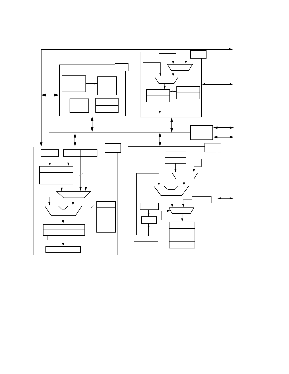
Figure 4 shows a block diagram of the DSP1628. The
following modules make up the DSP1628.
DSP1600 Core
The DSP1600 core is the heart of the DSP1628 chip.
The core contains data and address arithmetic units,
and control for on-chip memory and peripherals. The
core provides support for external memory wait-states
and on-chip dual-port RAM and features vectored interrupts and a trap mechanism.
Dual-Port RAM (DPRAM)
The DSP1628x16 contains 16 banks of zero wait-state
memory and the DSP1628x08 contains 8 banks of zero
wait-state memory. Each bank consists of 1K 16-bit
words and has separate address and data ports to the
instruction/coefficient and data memory spaces. A program can reference memory from either space. The
DSP1600 core automatically performs the required multiplexing. If references to both ports of a single bank are
made simultaneously, the DSP1600 core automatically
inserts a wait-state and performs the data port access
first, followed by the instruction/coefficient port access.
A program can be downloaded from slow, off-chip memory into DPRAM, and then executed without wait-states.
DPRAM is also useful for improving convolution performance in cases where the coefficients are adaptive.
Since DPRAM can be downloaded through the JTAG
port, full-speed remote in-circuit emulation is possible.
DPRAM can also be used for downloading self-test
code via the JTAG port.
Read-Only Memory (ROM)
The DSP1628 contains 48K 16-bit words of zero waitstate mask-programmable ROM for program and fixed
coefficients.
External Memory Multiplexer (EMUX)
The EMUX is used to connect the DSP1628 to external
memory and I/O devices. It supports read/write operations from/to instruction/coefficient memory (X memory
space) and data memory (Y memory space). The
DSP1600 core automatically controls the EMUX. Instructions can transparently reference external memory
from either set of internal buses. A sequencer allows a
single instruction to access both the X and the Y external memory spaces.
Clock Synthesis
The DSP powers up with a 1X input clock (CKI/CKI2) as
the source for the processor clock. An on-chip clock
synthesizer (PLL) can also be used to generate the system clock for the DSP, which will run at a frequency multiple of the input clock. The clock synthesizer is
deselected and powered down on reset. For low-power
operation, an internally generated slow clock can be
used to drive the DSP. If both the clock synthesizer and
the internally generated slow clock are selected, the
slow clock will drive the DSP; however, the synthesizer
will continue to run.
The clock synthesizer and other programmable clock
sources are discussed in Section 4.13. The use of these
programmable clock sources for power management is
discussed in Section 4.14.
8 Lucent Technologies Inc.

Preliminary Data Sheet
February 1997 DSP1628 Digital Signal Processor
4 Hardware Architecture (continued)
Bit Manipulation Unit (BMU)
The BMU extends the DSP1600 core instruction set to
provide more efficient bit operations on accumulators.
The BMU contains logic for barrel shifting, normalization, and bit field insertion/extraction. The unit also contains a set of 36-bit alternate accumulators. The data in
the alternate accumulators can be shuffled with the data
in the main accumulators. Flags returned by the BMU
mesh seamlessly with the DSP1600 conditional instructions.
Error Correction Coprocessor (ECCP)
The ECCP performs full Viterbi decoding with instructions for MLSE equalization and convolutional decoding. It is designed for 2-tap to 6-tap MLSE equalization
with Euclidean branch metrics and rate 1/1 to 1/6 convolutional decoding using constraint lengths from 2 to 7
with Euclidean or Manhattan branch metrics. Two variants of soft-decoded symbols, as well as hard-decoded
symbols may be programmed. The ECCP operates in
parallel with the DSP1600 core, increasing the throughput rate. Single instruction Viterbi decoding provides
significant code compression required for single DSP
solutions in modern digital cellular applications. The
ECCP is the source of two interrupts and one flag to the
DSP1600 core.
Bit Input/Output (BIO)
The BIO provides convenient and efficient monitoring
and control of eight individually configurable pins. When
configured as outputs, the pins can be individually set,
cleared, or toggled. When configured as inputs, individual pins or combinations of pins can be tested for patterns. Flags returned by the BIO mesh seamlessly with
conditional instructions.
Serial Input/Output Units (SIO and SIO2)
SIO and SIO2 offer asynchronous, full-duplex, doublebuffered channels that operate at up to 25 Mbits/s (for
20 ns instruction cycle in a nonmultiprocessor configuration), and easily interface with other Lucent Technologies fixed-point DSPs in a multiple-processor
environment. Commercially available codecs and timedivision multiplex (TDM) channels can be interfaced to
the serial I/O ports with few, if any, additional components. SIO2 is identical to SIO.
An 8-bit serial protocol channel may be transmitted in
addition to the address of the called processor in multiprocessor mode. This feature is useful for transmitting
high-level framing information or for error detection and
correction. SIO2 and BIO are pin-multiplexed with the
PHIF.
Lucent Technologies Inc. 9
Preliminary Data Sheet
DSP1628 Digital Signal Processor February 1997
4 Hardware Architecture (continued)
CKI
CKI2
CKO
RSTB
STOP
TRAP
INT[1:0]
IACK
VEC[3:0] OR IOBIT[7:4]
DO2 OR PSTAT
OLD2 OR PODS
OCK2 OR PCSN
OBE2 OR POBE
SYNC2 OR PBSEL
ICK2 OR PB0
ILD2 OR PIDS
DI2 OR PB1
IBF2 OR PIBF
DOEN2 OR PB2
SADD2 OR PB3
IO BIT[3:0] OR PB[7:4]
AB[15:0]DB[15:0]
ioc
ROM
48K x 16
DUAL-PORT
RAM
[16/8:5,3:1]
15/7K x 16
M
U
X
RWN EXM EROM ERAMHI
EXTERNAL MEMORY INTERFACE & EMUX
†
DSP1600 CORE
PHIF
phifc
*
PSTAT
pdx0(IN)
pdx0(OUT)
I/O
YAB YDBXDBXAB
IDB
powerc
BIO
sbit
cbit
pllc
RAM4
1K x 16
ECCP
eir
ear
edr
BMU
aa0
aa1
ar0
ar1
ar2
ar3
ERAMLO
†
sdx2(OUT)
sdx2(IN)
saddx2
SIO2
srta2
tdms2
sioc2
JTAG
BOUNDARY SCAN
jtag
*
JCON
*
ID
*
BYPASS
HDS
BREAK POINT
*
TRACE
TIMER
timerc
timer0
SIO
sdx(OUT)
srta
tdms
sdx(IN)
sioc
saddx
*
TDO
TDI
TCK
TMS
TRST
*
DI1
ICK1
ILD1
IBF1
DO1
OCK1
OLD1
OBE1
SYNC1
SADD1
DOEN1
5-4142 (F).f
* These registers are accessible through the pins only.
† 16K x 16 for the DSP1628x16, 8K x 16 for the DSP1628x08.
Figure 4. DSP1628 Block Diagram
10 Lucent Technologies Inc.

Preliminary Data Sheet
February 1997 DSP1628 Digital Signal Processor
4 Hardware Architecture (continued)
Table 2. DSP1628 Block Diagram Legend
Symbol Name
aa<0—1> Alternate Accumulators.
ar<0—3> Auxiliary BMU Registers.
BIO Bit Input/Output Unit.
BMU Bit Manipulation Unit.
BREAKPOINT Four Instruction Breakpoint Registers.
BYPASS JTAG Bypass Register.
cbit Control Register for BIO.
Dual-Port RAM Internal RAM (16 Kwords for DSP1628x16, 8 Kwords for DSP1628x08).
ECCP Error Correction Coprocessor.
ear Error Correction Coprocessor Address Register.
edr Error Correction Coprocessor Data Register.
eir Error Correction Coprocessor Instruction Register.
EMUX External Memory Multiplexer.
HDS Hardware Development System.
ID JTAG Device Identification Register.
IDB Internal Data Bus.
ioc I/O Configuration Register.
JCON JTAG Configuration Registers.
jtag 16-bit Serial/Parallel Register.
pdx0(in) Parallel Data Transmit Input Register 0.
pdx0(out) Parallel Data Transmit Output Register 0.
PHIF Parallel Host Interface.
phifc Parallel Host Interface Control Register.
pllc Phase-Locked Loop Control Register.
powerc Power Control Register.
PSTAT Parallel Host Interface Status Register.
saddx Multiprocessor Protocol Register.
saddx2 Multiprocessor Protocol Register for SIO2.
sbit Status Register for BIO.
sdx(in) Serial Data Transmit Input Register.
sdx2(in) Serial Data Transmit Input Register for SIO2.
sdx(out) Serial Data Transmit Output Register.
sdx2(out) Serial Data Transmit Output Register for SIO2.
SIO Serial Input/Output Unit.
SIO2 Serial Input/Output Unit #2.
sioc Serial I/O Control Register.
sioc2 Serial I/O Control Register for SIO2.
srta Serial Receive/Transmit Address Register.
srta2 Serial Receive/Transmit Address Register for SIO2.
tdms Serial I/O Time-division Multiplex Signal Control Register.
tdms2 Serial I/O Time-division Multiplex Signal Control Register for SIO2.
TIMER Programmable Timer.
timer0 Timer Running Count Register.
timerc Timer Control Register.
TRACE Program Discontinuity Trace Buffer.
XAB Program Memory Address Bus.
XDB Program Memory Data Bus.
YAB Data Memory Address Bus.
YDB Data Memory Data Bus.
Lucent Technologies Inc. 11

Preliminary Data Sheet
DSP1628 Digital Signal Processor February 1997
4 Hardware Architecture (continued)
Parallel Host Interface (PHIF)
The PHIF is a passive, 8-bit parallel port which can interface to an 8-bit bus containing other Lucent Technologies DSPs (e.g., DSP1620, DSP1627, DSP1628,
DSP1629, DSP1611, DSP1616, DSP1617, DSP1618),
microprocessors, or peripheral I/O devices. The PHIF
port supports either
as 8-bit or 16-bit transfers, configured in software. The
port data rate depends upon the instruction cycle rate.
A 25 ns instruction cycle allows the PHIF to support
data rates up to 11.85 Mbytes/s, assuming the external
host device can transfer 1 byte of data in 25 ns.
The PHIF is accessed in two basic modes, 8-bit or
16-bit mode. In 16-bit mode, the host determines an access of the high or low byte. In 8-bit mode, only the low
byte is accessed. Software-programmable features allow for a glueless host interface to microprocessors
(see Section 4.8, Parallel Host Interface).
Timer
The timer can be used to provide an interrupt at the expiration of a programmed interval. The interrupt may be
single or repetitive. More than nine orders of magnitude
of interval selection are provided. The timer may be
stopped and restarted at any time.
Hardware Development System (HDS) Module
The on-chip HDS performs instruction breakpointing
and branch tracing at full speed without additional offchip hardware. Using the JTAG port, the breakpointing
is set up, and the trace history is read back. The port
works in conjunction with the HDS code in the on-chip
ROM and the hardware and software in a remote computer. The HDS code must be linked to the user's application code and reside in the first 4 Kwords of ROM.
The on-chip HDS cannot be used with the secure ROM
masking option (see Section 7.2, ROM Security Options).
Four hardware breakpoints can be set on instruction addresses. A counter can be preset with the number of
breakpoints to receive before trapping the core. Breakpoints can be set in interrupt service routines. Alternately, the counter can be preset with the number of cache
instructions to execute before trapping the core.
Every time the program branches instead of executing
the next sequential instruction, the addresses of the instructions executed before and after the branch are
caught in circular memory. The memory contains the
last four pairs of program discontinuities for hardware
tracing.
In systems with multiple processors, the processors
may be configured such that any processor reaching a
breakpoint will cause all the other processors to be
trapped (see Section 4.3, Interrupts and Trap).
12 Lucent Technologies Inc.
Motorola
or
Intel
protocols, as well
Pin Multiplexing
In order to allow flexible device interfacing while maintaining a low package pin count, the DSP1628 multiplexes 16 package pins between BIO, PHIF, VEC[3:0],
and SIO2.
Upon reset, the vectored interrupt indication signals,
VEC[3:0], are connected to the package pins while
IOBIT[4:7] are disconnected. Setting bit 12, EBIOH, of
the ioc register connects IOBIT[4:7] to the package pins
and disconnects VEC[3:0].
Upon reset, the parallel host interface (PHIF) is connected to the package pins while the second serial port
(SIO2) and IOBIT[3:0] are disconnected. Setting bit 10,
ESIO2, of the ioc register connects the SIO2 and
IOBIT[3:0] and disconnects the PHIF.
Power Management
Many applications, such as portable cellular terminals,
require programmable sleep modes for power management. There are three different control mechanisms for
achieving low-power operation: the powerc control
register, the STOP pin, and the AWAIT bit in the alf register. The AWAIT bit in the alf register allows the processor to go into a power-saving standby mode until an
interrupt occurs. The powerc register configures various power-saving modes by controlling internal clocks
and peripheral I/O units. The STOP pin controls the internal processor clock. The various power management
options may be chosen based on power consumption
and/or wake-up latency requirements.
4.2 DSP1600 Core Architectural Overview
Figure 5 shows a block diagram of the DSP1600 core.
System Cache and Control Section (SYS)
This section of the core contains a 15-word cache memory and controls the instruction sequencing. It handles
vectored interrupts and traps, and also provides decoding for registers outside of the DSP1600 core. SYS
stretches the processor cycle if wait-states are required
(wait-states are programmable for external memory accesses). SYS sequences downloading via JTAG of selftest programs to on-chip, dual-port RAM.
The cache loop iteration count can be specified at run
time under program control as well as at assembly time.

Preliminary Data Sheet
February 1997 DSP1628 Digital Signal Processor
4 Hardware Architecture (continued)
Data Arithmetic Unit (DAU)
The data arithmetic unit (DAU) contains a 16 x 16-bit
parallel multiplier that generates a full 32-bit product in
one instruction cycle. The product can be accumulated
with one of two 36-bit accumulators. The accumulator
data can be directly loaded from, or stored to, memory
in two 16-bit words with optional saturation on overflow.
The arithmetic logic unit (ALU) supports a full set of
arithmetic and logical operations on either 16- or 32-bit
data. A standard set of flags can be tested for conditional ALU operations, branches, and subroutine calls. This
procedure allows the processor to perform as a powerful 16- or 32-bit microprocessor for logical and control
applications. The available instruction set is compatible
with the DSP1618 instruction set. See Section 5.1 for
more information on the instruction set.
The user also has access to two additional DAU registers. The psw register contains status information from
the DAU (see Table 30, Processor Status Word Register). The arithmetic control register, auc, is used to configure some of the features of the DAU (see Table 31)
including single-cycle squaring. The auc register alignment field supports an arithmetic shift left by one and
left or right by two. The auc register is cleared by reset.
The counters c0 to c2 are signed, 8 bits wide, and may
be used to count events such as the number of times
the program has executed a sequence of code. They
are controlled by the conditional instructions and provide a convenient method of program looping.
The YAAU allows direct (or indexed) addressing of data
memory. In direct addressing, the 16-bit base register
(ybase) supplies the 11 most significant bits of the address. The direct data instruction supplies the remaining
5 bits to form an address to Y memory space and also
specifies one of 16 registers for the source or destination.
X Space Address Arithmetic Unit (XAAU)
The XAAU supports high-speed, register-indirect, instruction/coefficient memory addressing with postmodification of the register. The 16-bit pt register is used for
addressing coefficients. The signed register i holds a
user-defined postincrement. A fixed postincrement of
+1 is also available. Register PC is the program
counter. Registers pr and pi hold the return address for
subroutine calls and interrupts, respectively.
The XAAU decodes the 16-bit instruction/coefficient address and produces enable signals for the appropriate
X memory segment. The addressable X segments are
48 Kwords of internal ROM, up to 16 Kwords of DPRAM
for the DSP1628x16 or up to 8 Kwords of DPRAM for
the DSP1628x08, and external ROM.
The locations of these memory segments depend upon
the memory map selected (see Table 5). A security
mode can be selected by mask option. This prevents
unauthorized access to the contents of on-chip ROM
(see Section 7, Mask-Programmable Options).
4.3 Interrupts and Trap
Y Space Address Arithmetic Unit (YAAU)
The YAAU supports high-speed, register-indirect, compound, and direct addressing of data (Y) memory. Four
general-purpose, 16-bit registers, r0 to r3, are available
in the YAAU. These registers can be used to supply the
read or write addresses for Y space data. The YAAU
also decodes the 16-bit data memory address and outputs individual memory enables for the data access.
The YAAU can address the six 1 Kword banks of onchip DPRAM or three external data memory segments.
Up to 48 Kwords of off-chip RAM are addressable, with
16K addresses reserved for internal RAM.
Two 16-bit registers, rb and re, allow zero-overhead
modulo addressing of data for efficient filter implementations. Two 16-bit signed registers, j and k, are used to
hold user-defined postmodification increments. Fixed
increments of +1, –1, and +2 are also available. Four
compound-addressing modes are provided to make
read/write operations more efficient.
The DSP1628 supports prioritized, vectored interrupts
and a trap. The device has eight internal hardware
sources of program interrupt and two external interrupt
pins. Additionally, there is a trap pin and a trap signal
from the hardware development system (HDS). A software interrupt is available through the icall instruction.
The icall instruction is reserved for use by the HDS.
Each of these sources of interrupt and trap has a unique
vector address and priority assigned to it. DSP16A interrupt compatibility is not maintained.
The software interrupt and the traps are always enabled
and do not have a corresponding bit in the ins register.
Other vectored interrupts are enabled in the inc register
(see Table 33, Interrupt Control (inc) Register) and
monitored in the ins register (see Table 34, Interrupt
Status (ins) Register). When the DSP1628 goes into an
interrupt or trap service routine, the IACK pin is asserted. In addition, pins VEC[3:0] encode which interrupt/
trap is being serviced. Table 4 details the encoding
used for VEC[3:0].
Lucent Technologies Inc. 13
Preliminary Data Sheet
DSP1628 Digital Signal Processor February 1997
4 Hardware Architecture (continued)
CONTROL
x (16)
16 x 16 MPY
SHIFT (–2, 0, 1, 2)
EXTRACT/SAT
yh (16)
p (32)
ALU/SHIFT
a0 (36)
a1 (36)
16
MUX
ins (16)
inc (16)
32
yl (16)
36
CACHE
cloop (7)
alf (16)
mwait (16)
DAU
c0 (8)
c1 (8)
c2 (8)
auc (16)
psw (16)
SYS
re (16)
CMP
ybase (16)
ADDER
pc (16)
pt (16)
i (16)
k (16)
ADDER
j (16)
MUX
pr (16)
pi (16)
MUX
MUX
r0 (16)
r1 (16)
r2 (16)
r3 (16)
1
XAAU
BRIDGE
–1, 0, 1, 2
rb (16)
XDB
XAB
IDB
YDB
YAAU
YAB
5-1741 (F).b
Figure 5. DSP1600 Core Block Diagram
14 Lucent Technologies Inc.

Preliminary Data Sheet
February 1997 DSP1628 Digital Signal Processor
4 Hardware Architecture (continued)
Table 3. DSP1600 Core Block Diagram Legend
Symbol Name
16 x 16 MPY 16-bit x 16-bit Multiplier.
a0—a1 Accumulators 0 and 1 (16-bit halves specified as a0, a0l, a1, and a1l)*.
alf AWAIT, LOWPR, Flags.
ALU/SHIFT Arithmetic Logic Unit/Shifter.
auc Arithmetic Unit Control.
c0—c2 Counters 0—2.
cloop Cache Loop Count.
CMP Comparator.
DAU Digital Arithmetic Unit.
i Increment Register for the X Address Space.
IDB Internal Data Bus.
inc Interrupt Control.
ins Interrupt Status.
j Increment Register for the Y Address Space.
k Increment Register for the Y Address Space.
MUX Multiplexer.
mwait External Memory Wait-states Register.
p Product Register (16-bit halves specified as p, pl).
PC Program Counter.
pi Program Interrupt Return Register.
pr Program Return Register.
psw Processor Status Word.
pt X Address Space Pointer.
r0—r3 Y Address Space Pointers.
rb Modulo Addressing Register (begin address).
re Modulo Addressing Register (end address).
SYS System Cache and Control Section.
x Multiplier Input Register.
XAAU X Space Address Arithmetic Unit.
XAB X Space Address Bus.
XDB X Space Data Bus.
YAAU Y Space Address Arithmetic Unit.
YAB Y Space Address Bus.
YDB Y Space Data Bus.
ybase Direct Addressing Base Register.
y DAU Register (16-bit halves specified as y, yl).
* F3 ALU instructions with immediates require specifying the high half of the accumulators as a0h and a1h.
Lucent Technologies Inc. 15

Preliminary Data Sheet
DSP1628 Digital Signal Processor February 1997
4 Hardware Architecture (continued)
Interruptibility
Vectored interrupts are serviced only after the execution
of an interruptible instruction. If more than one
vectored interrupt is asserted at the same time, the interrupts are serviced sequentially according to their assigned priorities. See Table 4 for the priorities assigned
to the vectored interrupts. Interrupt service routines,
branch and conditional branch instructions, cache
loops, and instructions that only decrement one of the
RAM pointers, r0 to r3 (e.g., *r3− −), are not interruptible.
A trap is similar to an interrupt, but it gains control of the
processor by branching to the trap service routine even
when the current instruction is noninterruptible. It may
not be possible to return to normal instruction execution
from the trap service routine since the machine state
cannot always be saved. In particular, program execution cannot be continued from a trapped cache loop or
interrupt service routine. While in a trap service routine,
another trap is ignored.
When set to 1, the status bits in the ins register indicate
that an interrupt has occurred. The processor must
reach an interruptible state (completion of an interruptible instruction) before an enabled vectored interrupt will
be acted on. An interrupt will not be serviced if it is not
enabled. Polled interrupt service can be implemented
by disabling the interrupt in the inc register and then
polling the ins register for the expected event.
Vectored Interrupts
Tables 33 and 34 show the inc and ins registers. A logic
1 written to any bit of inc enables (or unmasks) the associated interrupt. If the bit is cleared to a logic 0, the interrupt is masked. Note that neither the software
interrupt nor traps can be masked.
The occurrence of an interrupt that is not masked will
cause the program execution to transfer to the memory
location pointed to by that interrupt's vector address,
assuming no other interrupt is being serviced (see
Table 4, Interrupt Vector Table). The occurrence of an
interrupt that is masked causes no automatic processor
action, but will set the corresponding status bit in the ins
register. If a masked interrupt occurs, it is latched in the
ins register, but the interrupt is not taken. When unlatched, this latched interrupt will initiate automatic processor interrupt action. See the
Digital Signal Processor Information Manual
detailed description of the interrupts.
DSP1611/17/18/27
for a more
Signaling Interrupt Service Status
Five pins of DSP1628 are devoted to signaling interrupt
service status. The IACK pin goes high while any interrupt or user trap is being serviced, and goes low when
the ireturn instruction from the service routine is issued.
Four pins, VEC[3:0], carry a code indicating which of the
interrupts or trap is being serviced. Table 4 contains the
encodings used by each interrupt.
Traps due to HDS breakpoints have no effect on either
the IACK or VEC[3:0] pins. Instead, they show the interrupt state or interrupt source of the DSP when the trap
occurred.
Clearing Interrupts
The PHIF interrupts (PIBF and POBE) are cleared by
reading or writing the parallel host interface data transmit registers pdx0[in] and pdx0[out], respectively. The
SIO and SIO2 interrupts (IBF, IBF2, OBE, and OBE2)
are cleared one instruction cycle AFTER reading or writing the serial data registers, (sdx[in], sdx2[in], sdx[out],
or sdx2[out]). To account for this added latency, the
user must ensure that a single instruction (NOP or any
other valid DSP16XX instruction) follows the sdx register read or write instruction prior to exiting an interrupt
service routine (via an ireturn or goto pi instruction) or
before checking the ins register for the SIO flag status.
Adding this instruction ensures that interrupts are not
reported incorrectly following an ireturn or that stale
flags are not read from the ins register.The JTAG interrupt (JINT) is cleared by reading the jtag register.
Five of the vectored interrupts are cleared by writing to
the ins register. Writing a 1 to the INT0, INT1, EREADY,
EOVF, or TIME bits in the ins will cause the corresponding interrupt status bit to be cleared to a logic 0.
The status bit for these vectored interrupts is also
cleared when the ireturn instruction is executed, leaving
set any other vectored interrupts that are pending.
Traps
The TRAP pin of the DSP1628 is a bidirectional signal.
At reset, it is configured as an input to the processor.
Asserting the TRAP pin will force a user trap. The trap
mechanism is used for two purposes. It can be used by
an application to rapidly gain control of the processor for
asynchronous time-critical event handling (typically for
catastrophic error recovery). It is also used by the HDS
for breakpointing and gaining control of the processor.
Separate vectors are provided for the user trap (0x46)
and the HDS trap (0x3). Traps are not maskable.
16 Lucent Technologies Inc.

Preliminary Data Sheet
February 1997 DSP1628 Digital Signal Processor
4 Hardware Architecture (continued)
Table 4. Interrupt Vector Table
Source Vector Priority VEC[3:0] Issued by
No Interrupt — — 0x0 —
Software Interrupt 0x2 1 0x1 icall
INT0 0x1 2 0x2 pin
JINT 0x42 3 0x8 jtag in
INT1 0x4 4 0x9 pin
TIME 0x10 7 0xc timer
IBF2 0x14 8 0xd SIO2 in
OBE2 0x18 9 0xe SIO2 out
Reserved 0x1c 10 0x0 —
EREADY 0x20 11 0x1 ECCP ready
EOVF 0x24 12 0x2 ECCP overflow
IBF 0x2c 14 0x3 SIO in
OBE 0x30 15 0x4 SIO out
PIBF 0x34 16 0x5 PHIF in
POBE 0x38 17 0x6 PHIF out
TRAP from HDS 0x3 18 * breakpoint, jtag, or pin
TRAP from User 0x46 19 = highest 0x7 pin
* Traps due to HDS breakpoints have no effect on VEC[3:0] pins.
A trap has four cycles of latency. At most, two instructions will execute from the time the trap is received at
the pin to when it gains control. An instruction that is executing when a trap occurs is allowed to complete before the trap service routine is entered. (Note that the
instruction could be lengthened by wait-states.) During
normal program execution, the pi register contains either the address of the next instruction (two-cycle instruction executing) or the address following the next
instruction (one-cycle instruction executing). In an interrupt service routine, pi contains the interrupt return address. When a trap occurs during an interrupt service
routine, the value of the pi register may be overwritten.
Specifically, it is not possible to return to an interrupt
service routine from a user trap (0x46) service routine.
Continuing program execution when a trap occurs during a cache loop is also not possible.
The HDS trap causes circuitry to force the program
memory map to MAP1 (with on-chip ROM starting at address 0x0) when the trap is taken. The previous memory map is restored when the trap service routine exits by
issuing an ireturn. The map is forced to MAP1 because
the HDS code, if present, resides in the on-chip ROM.
Using the Lucent Technologies development tools, the
TRAP pin may be configured to be an output, or an input
vectoring to address 0x3. In a multiprocessor environment, the TRAP pins of all the DSPs present can be tied
together. During HDS operations, one DSP is selected
by the host software to be the master. The master processor's TRAP pin is configured to be an output.
The TRAP pins of the slave processors are configured
as inputs. When the master processor reaches a breakpoint, the master's TRAP pin is asserted. The slave processors will respond to their TRAP input by beginning to
execute the HDS code.
AWAIT Interrupt (Standby or Sleep Mode)
Setting the AWAIT bit (bit 15) of the alf register
(alf = 0x8000) causes the processor to go into a powersaving standby or sleep mode. Only the minimum circuitry on the chip required to process an incoming interrupt remains active. After the AWAIT bit is set, one
additional instruction will be executed before the standby power-saving mode is entered. A PHIF or SIO word
transfer will complete if already in progress. The AWAIT
bit is reset when the first interrupt occurs. The chip then
wakes up and continues executing.
Two nop instructions should be programmed after the
AWAIT bit is set. The first nop (one cycle) will be executed before sleeping; the second will be executed after
the interrupt signal awakens the DSP and before the interrupt service routine is executed.
Lucent Technologies Inc. 17

Preliminary Data Sheet
DSP1628 Digital Signal Processor February 1997
4 Hardware Architecture (continued)
The AWAIT bit should be set from within the cache if the
code which is executing resides in external ROM where
more than one wait-state has been programmed. This
ensures that an interrupt will not disturb the device from
completely entering the sleep state.
For additional power savings, set ioc = 0x0180 and tim-
erc = 0x0040 in addition to setting alf = 0x8000. This
will hold the CKO pin low and shut down the timer and
prescaler (see Table 42 and Table 35).
For a description of the control mechanisms for putting
the DSP into low-power modes, see Section 4.13, Power Management.
4.4 Memory Maps and Wait-States
The DSP1600 core implements a modified Harvard architecture that has separate on-chip 16-bit address and
data buses for the instruction/coefficient (X) and data
(Y) memory spaces. Table 5 shows the instruction/coefficient memory space maps for both the DSP1628x16
and DSP1628x08.
The DSP1628 provides a multiplexed external bus
which accesses external RAM (ERAM) and ROM (EROM). Programmable wait-states are provided for external memory accesses. The instruction/coefficient
memory map is configurable to provide application flexibility. Table 6 shows the data memory space, which
has one map.
Instruction/Coefficient Memory Map Selection
In determining which memory map to use, the processor evaluates the state of two parameters. The first is
the LOWPR bit (bit 14) of the alf register. The LOWPR
bit of the alf register is initialized to 0 automatically at reset. LOWPR controls the starting address in memory
assigned to 1K banks of dual-port RAM. If LOWPR is
low, internal dual-port RAM begins at address 0xC000.
If LOWPR is high, internal dual-port RAM begins at address 0x0. LOWPR also moves IROM from 0x0 in
MAP1 to 0x4000 in MAP3, and EROM from 0x0 in
MAP2 to 0x4000 in MAP4.
The second parameter is the value at reset of the EXM
pin (pin 27 or pin 14, depending upon the package
type). EXM determines whether the internal 48 Kwords
ROM (IROM) will be addressable in the memory map.
The Lucent Technologies development system tools,
together with the on-chip HDS circuitry and the JTAG
port, can independently set the memory map. Specifically, during an HDS trap, the memory map is forced to
MAP1. The user's map selection is restored when the
trap service routine has completed execution.
MAP1
MAP1 has the IROM starting at 0x0 and 1 Kword banks
of DPRAM starting at 0xC000. MAP1 is used if
DSP1628 has EXM low at reset and the LOWPR parameter is programmed to zero. It is also used during an
HDS trap.
MAP2
MAP2 differs from MAP1 in that the lowest 48 Kwords
reference external ROM (EROM). MAP2 is used if EXM
is high at reset, the LOWPR parameter is programmed
to zero, and an HDS trap is not in progress.
MAP3
MAP3 has the 1 Kword banks of DPRAM starting at
address 0x0. In MAP3, the 48 Kwords of IROM start at
0x4000. MAP3 is used if EXM is low at reset, the
LOWPR bit is programmed to 1, and an HDS trap is not
in progress. Note that this map is not available if the
secure mask-programmable option has been ordered.
MAP4
MAP4 differs from MAP3 in that addresses above
0x4000 reference external ROM (EROM). This map is
used if the LOWPR bit is programmed to 1, an HDS trap
is not in progress, and, either EXM is high during reset,
or the secure mask-programmable option has been ordered.
Whenever the chip is reset using the RSTB pin, the default memory map will be MAP1 or MAP2, depending
upon the state of the EXM pin at reset. A reset through
the HDS will not reinitialize the alf register, so the previous memory map is retained.
Boot from External ROM
After RSTB goes from low to high, the DSP1628 comes
out of reset and fetches an instruction from address
zero of the instruction/coefficient space. The physical
location of address zero is determined by the memory
map in effect. If EXM is high at the rising edge of RSTB,
MAP2 is selected. MAP2 has EROM at location zero;
thus, program execution begins from external memory.
If EXM is high and INT1 is low when RSTB rises, the
mwait register defaults to 15 wait-states for all external
memory segments. If INT1 is high, the mwait register
defaults to 0 wait-states.
18 Lucent Technologies Inc.

Preliminary Data Sheet
February 1997 DSP1628 Digital Signal Processor
4 Hardware Architecture (continued)
Table 5. Instruction/Coefficient Memory Maps
DSP1628x16
MAP 3
EXM = 0
DPRAM
(16K)
IROM
(48K)
‡
MAP 4
EXM = 1
LOWPR = 1
DPRAM
(16K)
EROM
(48K)
X Address AB[0:15]
0 0x0000
4K 0x1000
8K 0x2000
12K 0x3000
16K 0x4000
20K 0x5000
24K 0x6000
28K 0x7000
32K 0x8000
36K 0x9000
40K 0xA000
44K 0xB000
48K 0xC000
52K 0xD000
54K 0xD800
56K 0xE000
60K—64K 0xFFFF
MAP 1*
EXM = 0
LOWPR = 0
IROM
(48K)
DPRAM
(16K)
†
MAP 2
EXM = 1
LOWPR = 0
EROM
(48K)
DPRAM
(16K)
LOWPR = 1
DSP1628x08
MAP 1*
X Address AB[0:15]
0 0x0000
4K 0x1000
6K 0x1800
8K 0x2000
12K 0x3000
16K 0x4000
20K 0x5000
24K 0x6000
28K 0x7000
32K 0x8000
36K 0x9000
40K 0xA000
44K 0xB000
48K 0xC000
52K 0xD000
54K 0xD800
56K 0xE000
58K 0xE800
60K—64K 0xFFFF
* MAP1 is set automatically during an HDS trap. The user-selected map is restored at the end of the HDS trap service routine.
† LOWPR is an alf register bit. The Lucent Technologies development system tools can independently set the memory map.
‡ MAP3 is not available if the secure mask-programmable option is selected.
EXM = 0
LOWPR = 0
IROM
(48K)
DPRAM
(8K)
Reserved
(8K)
†
MAP 2
EXM = 1
LOWPR = 0
EROM
(48K)
DPRAM
(8K)
Reserved
(8K)
LOWPR = 1
Reserved
MAP 3
EXM = 0
DPRAM
(8K)
(8K)
IROM
(48K)
‡
MAP 4
EXM = 1
LOWPR = 1
DPRAM
(8K)
Reserved
(8K)
EROM
(48K)
Lucent Technologies Inc. 19

Preliminary Data Sheet
DSP1628 Digital Signal Processor February 1997
4 Hardware Architecture (continued)
Table 6. Data Memory Maps
1628x16 Data Memory Map (Not to Scale)
1628x08 Data Memory Map (Not to Scale)
Decimal
Address
0 0x0000 DPRAM[1:16]
16K 0x4000 IO
16,640 0x4100 ERAMLO
32K 0x8000 ERAMHI
Address in
r0, r1, r2, r3
Segment
Decimal
Address
0 0x0000 DPRAM[1:8]
8K 0x2000 Reserved
16K 0x4000 IO
16,640 0x4100 ERAMLO
32K 0x8000 ERAMHI
Address in
r0, r1, r2, r3
Segment
64K – 1 0xFFFF
On the data memory side (see Table ), the 1K banks of
dual-port RAM are located starting at address 0. Addresses from 0x4000 to 0x40FF reference a 256-word
memory-mapped I/O segment (IO). Addresses from
0x4100 to 0x7FFF reference the low external data RAM
segment (ERAMLO). Addresses above 0x8000 reference high external data RAM (ERAMHI).
20 Lucent Technologies Inc.
64K – 1 0xFFFF
Wait-States
The number of wait-states (from 0 to 15) used when accessing each of the four external memory segments
(ERAMLO, IO, ERAMHI, and EROM) is programmable
in the mwait register (see Table 40). When the program
references memory in one of the four external segments, the internal multiplexer is automatically switched
to the appropriate set of internal buses, and the associated external enable of ERAMLO, IO, ERAMHI, or
EROM is issued. The external memory cycle is automatically stretched by the number of wait-states configured in the appropriate field of the mwait register.

Preliminary Data Sheet
February 1997 DSP1628 Digital Signal Processor
4 Hardware Architecture (continued)
4.5 External Memory Interface (EMI)
The external memory interface supports read/write operations from instruction/coefficient memory, data
memory, and memory-mapped I/O devices. The
DSP1628 provides a 16-bit external address bus,
AB[15:0], and a 16-bit external data bus, DB[15:0].
These buses are multiplexed between the internal buses for the instruction/coefficient memory and the data
memory. Four external memory segment enables,
ERAMLO, IO, ERAMHI, and EROM, select the external
memory segment to be addressed.
If a data memory location with an address between
0x4100 and 0x7FFF is addressed, ERAMLO is asserted
low.
If one of the 256 external data memory locations, with
an address greater than or equal to 0x4000, and less
than or equal to 0x40FF, is addressed, IO is asserted
low. IO is intended for memory-mapped I/O.
If a data memory location with an address greater than
or equal to 0x8000 is addressed, ERAMHI is asserted
low. When the external instruction/coefficient memory is
addressed, EROM is asserted low.
The flexibility provided by the programmable options of
the external memory interface (see Table 40, mwait
Register and Table 42, ioc Register) allows the
DSP1628 to interface gluelessly with a variety of commercial memory chips.
Each of the four external memory segments, ERAMLO,
IO, ERAMHI, and EROM, has a number of wait-states
that is programmable (from 0 to 15) by writing to the
mwait register. When the program references memory
in one of the four external segments, the internal multiplexer is automatically switched to the appropriate set of
internal buses, and the associated external enable of
ERAMLO, IO, ERAMHI, or EROM is issued. The external memory cycle is automatically stretched by the number of wait-states in the appropriate field of the mwait
register.
When writing to external memory, the RWN pin goes
low for the external cycle. The external data bus,
DB[15:0], is driven by the DSP1628 starting halfway
through the cycle. The data driven on the external data
bus is automatically held after the cycle for one additional clock period unless an external read cycle immediately follows.
The DSP1628 has one external address bus and one
external data bus for both memory spaces. Since some
instructions provide the capability of simultaneous access to both X space and Y space, some provision must
be made to avoid collisions for external accesses. The
DSP1628 has a sequencer that does the external X access first, and then the external Y access, transparently
to the programmer. Wait-states are maintained as programmed in the mwait register. For example, let two in-
structions be executed: the first reads a coefficient from
EROM and writes data to ERAM; the second reads a
coefficient from EROM and reads data from ERAM. The
sequencer carries out the following steps at the external
memory interface: read EROM, write ERAM, read EROM, and read ERAM. Each step is done in sequential
one-instruction cycle steps, assuming zero wait-states
are programmed. Note that the number of instruction
cycles taken by the two instructions is four. Also, in this
case, the write hold time is zero.
The DSP1628 allows writing into external instruction/
coefficient memory. By setting bit 11, WEROM, of the
ioc register (see Table 42), writing to (or reading from)
data memory or memory-mapped I/O asserts the
EROM strobe instead of ERAMLO, IO, or ERAMHI.
Therefore, with WEROM set, EROM appears in both Y
space (replacing ERAM) and X space, in its normal position.
Bit 14 of the ioc register (see Table 42), EXTROM, may
be used with WEROM to download to a full 64K of external memory. When WEROM and EXTROM are both
asserted, address bit 15 (AB15) is held low, aliasing the
upper 32K of external memory into the lower 32K.
When an access to internal memory is made, the
AB[15:0] bus holds the last valid external memory address. Asserting the RSTB pin low 3-states the AB[15:0]
bus. After reset, the AB[15:0] value is undefined.
The leading edge of the memory segment enables can
be delayed by approximately one-half a CKO period by
programming the ioc register (see Table 42). This is
used to avoid a situation in which two devices drive the
data bus simultaneously.
Bits 7, 8, and 13 of the ioc register select the mode of
operation for the CKO pin (see Table 42). Available options are a free-running unstretched clock, a wait-stated
sequenced clock (runs through two complete cycles
during a sequenced external memory access), and a
wait-stated clock based on the internal instruction cycle.
These clocks drop to the low-speed internal ring oscillator when SLOWCKI is enabled (see 4.13, Power Management). The high-to-low transitions of the wait-stated
clock are synchronized to the high-to-low transition of
the free-running clock. Also, the CKO pin provides either a continuously high level, a continuously low level,
or changes at the rate of the internal processor clock.
This last option, only available with the small-signal input clock options, enables the DSP1628 CKI input buffer to deliver a full-rate clock to other devices while the
DSP1628 itself is in one of the low-power modes.
Lucent Technologies Inc. 21

Preliminary Data Sheet
DSP1628 Digital Signal Processor February 1997
4 Hardware Architecture (continued)
4.6 Bit Manipulation Unit (BMU)
The BMU interfaces directly to the main accumulators in
the DAU providing the following features:
■ Barrel shifting—logical and arithmetic, left and right
shift
■ Normalization and extraction of exponent
■ Bit-field extraction and insertion
These features increase the efficiency of the DSP in applications such as control or data encoding and decoding. For example, data packing and unpacking, in which
short data words are packed into one 16-bit word for
more efficient memory storage, is very easy.
In addition, the BMU provides two auxiliary accumulators, aa0 and aa1. In one instruction cycle, 36-bit data
can be shuffled, or swapped, between one of the main
accumulators and one of the alternate accumulators.
The ar<0—3> registers are 16-bit registers that control
the operations of the BMU. They store a value that determines the amount of shift or the width and offset
fields for bit extraction or insertion. Certain operations in
the BMU set flags in the DAU psw register and the alf
register (see Table 30, Processor Status Word (psw)
Register, and Table 39, alf Register). The ar<0—3>
registers can also be used as general-purpose registers.
The BMU instructions are detailed in Section 5.1. For a
thorough description of the BMU, see the
18/27 Digital Signal Processor Information Manual
4.7 Serial I/O Units (SIOs)
DSP1611/17/
.
ercise loopback, the SIO clocks (ICK1, ICK2, OCK1,
and OCK2) should either all be in the active mode,
16-bit condition, or each pair should be driven from one
external source in passive mode. Similarly, pins ILD1
(ILD2) and OLD1 (OLD2) must both be in active mode
or tied together and driven from one external frame
clock in passive mode. During loopback, DO1, DO2,
DI1, DI2, ICK1, ICK2, OCK1, OCK2, ILD1, ILD2, OLD1,
OLD2, SADD1, SADD2, SYNC1, SYNC2, DOEN1, and
DOEN2 are 3-stated.
Setting DODLY = 1 (sioc and sioc2) delays DO by one
phase of OCK so that DO changes on the falling edge
of OCK instead of the rising edge (DODLY = 0). This reduces the time available for DO to drive DI and to be valid for the rising edge of ICK, but increases the hold time
on DO by half a cycle on OCK.
Programmable Modes
Programmable modes of operation for the SIO and
SIO2 are controlled by the serial I/O control registers
(sioc and sioc2). These registers, shown in Table 26,
are used to set the ports into various configurations.
Both input and output operations can be independently
configured as either active or passive. When active, the
DSP1628 generates load and clock signals. When passive, load and clock signal pins are inputs.
Since input and output can be independently configured, each SIO has four different modes of operation.
Each of the sioc registers is also used to select the frequency of active clocks for that SIO. Finally, these registers are used to configure the serial I/O data formats.
The data can be 8 or 16 bits long, and can also be input/
output MSB first or LSB first. Input and output data formats can be independently configured.
Multiprocessor Mode
The serial I/O ports on the DSP1628 device provide a
serial interface to many codecs and signal processors
with little, if any, external hardware required. Each highspeed, double-buffered port (sdx and sdx2) supports
back-to-back transmissions of data. SIO and SIO2 are
identical. The output buffer empty (OBE and OBE2) and
input buffer full (IBF and IBF2) flags facilitate the reading and/or writing of each serial I/O port by programor interrupt-driven I/O. There are four selectable active
clock speeds.
A bit-reversal mode provides compatibility with either
the most significant bit (MSB) first or least significant bit
(LSB) first serial I/O formats (see Table 26, Serial I/O
Control Registers (sioc and sioc2)). A multiprocessor
I/O configuration is supported. This feature allows up to
eight DSP161X devices to be connected together on an
SIO port without requiring external glue logic.
The serial data may be internally looped back by setting
the SIO loopback control bit, SIOLBC, of the ioc register. SIOLBC affects both the SIO and SIO2. The data
output signals are wrapped around internally from the
output to the input (DO1 to DI1 and DO2 to DI2). To ex-
22 Lucent Technologies Inc.
The multiprocessor mode allows up to eight devices
that support multiprocessor mode (codecs or DSP16XX
devices) to be connected together to provide data transmission among any of the multiprocessor devices in the
system. Either of the DSP1628’s SIO ports (SIO or
SIO2) may be independently used for the multiprocessor mode. The multiprocessor interface is a four-wire interface, consisting of a data channel, an address/
protocol channel, a transmit/receive clock, and a sync
signal (see Figure 6). The DI1 and DO1 pins of all the
DSPs are connected to transmit and receive the data
channel. The SADD1 pins of all the DSPs are connected to transmit and receive the address/protocol channel. ICK1 and OCK1 should be tied together and driven
from one source. The SYNC1 pins of all the DSPs are
connected.
In the configuration shown in Figure 6, the master DSP
(DSP0) generates active SYNC1 and OCK1 signals
while the slave DSPs use the SYNC1 and OCK1 signals
in passive mode to synchronize operations. In addition,
all DSPs must have their ILD1 and OLD1 signals in active mode.

Preliminary Data Sheet
February 1997 DSP1628 Digital Signal Processor
4 Hardware Architecture (continued)
While ILD1 and OLD1 are not required externally for
multiprocessor operation, they are used internally in the
DSP's SIO. Setting the LD field of the master's sioc register to a logic level 1 will ensure that the active generation of SYNC1, ILD1, and OLD1 is derived from OCK1
(see Table 26). With this configuration, all DSPs should
use ICK1 (tied to OCK1) in passive mode to avoid conflicts on the clock (CK) line (see the
Digital Signal Processor Information Manual
information).
Four registers (per SIO) configure the multiprocessor
mode: the time-division multiplexed slot register (tdms
or tdms2), the serial receive and transmit address register (srta or srta2), the serial data transmit register
(sdx or sdx2), and the multiprocessor serial address/
protocol register (saddx or saddx2).
Multiprocessor mode requires no external logic and
uses a TDM interface with eight 16-bit time slots per
frame. The transmission in any time slot consists of
16 bits of serial data in the data channel and 16 bits of
address and protocol information in the address/protocol channel. The address information consists of the
transmit address field of the srta register of the transmitting device. The address information is transmitted
concurrently with the transmission of the first 8 bits of
data. The protocol information consists of the transmit
protocol field written to the saddx register and is transmitted concurrently with the last 8 bits of data (see
Table 29, Multiprocessor Protocol Register). Data is received or recognized by other DSP(s) whose receive
address matches the address in the address/protocol
channel. Each SIO port has a user-programmable receive address and transmit address associated with it.
The transmit and receive addresses are programmed in
the srta register.
In multiprocessor mode, each device can send data in
a unique time slot designated by the tdms register
transmit slot field (bits 7—0). The tdms register has a
fully decoded transmit slot field in order to allow one
DSP1628 device to transmit in more than one time slot.
This procedure is useful for multiprocessor systems
with less than eight DSP1628 devices when a higher
bandwidth is necessary between certain devices in that
system. The DSP operating during time slot 0 also
drives SYNC1.
DSP1611/17/18/27
for more
In order to prevent multiple bus drivers, only one DSP
can be programmed to transmit in a particular time slot.
In addition, it is important to note that the address/protocol channel is 3-stated in any time slot that is not being
driven.
Therefore, to prevent spurious inputs, the address/protocol channel should be pulled up to VDD with a 5 kΩ resistor, or it should be guaranteed that the bus is driven
in every time slot. (If the SYNC1 signal is externally generated, then this pull-up is required for correct initialization.)
Each SIO also has a fully decoded transmitting address
specified by the srta register transmit address field (bits
7—0). This is used to transmit information regarding the
destination(s) of the data. The fully decoded receive address specified by the srta register receive address field
(bits 15—8) determines which data will be received. The
SIO protocol channel data is controlled via the saddx
register. When the saddx register is written, the lower 8
bits contain the 8-bit protocol field. On a read, the highorder 8 bits read from saddx are the most recently received protocol field sent from the transmitting DSP's
saddx output register. The low-order 8 bits are read as
0s.
An example use of the protocol channel is to use the top
3 bits of the saddx value as an encoded source address
for the DSPs on the multiprocessor bus. This leaves the
remaining 5 bits available to convey additional control
information, such as whether the associated field is an
opcode or data, or whether it is the last word in a transfer, etc. These bits can also be used to transfer parity information about the data. Alternatively, the entire field
can be used for data transmission, boosting the bandwidth of the port by 50%.
Using SIO2
The SIO2 functions the same as the SIO. Please refer
to Pin Multiplexing in Section 4.1 for a description of pin
multiplexing of BIO, PHIF, VEC[3:0], and SIO2.
Lucent Technologies Inc. 23
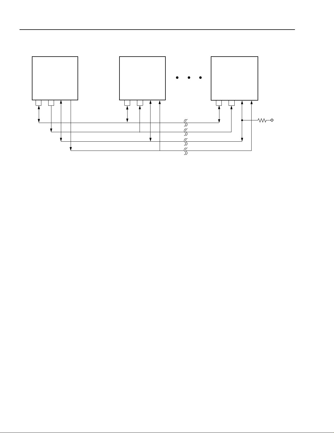
Preliminary Data Sheet
DSP1628 Digital Signal Processor February 1997
4 Hardware Architecture (continued)
DO
DI
DSP 0
ICK
OCK
SADD
SYNC
DATA CHANNEL
CLOCK
ADDRESS/PROTOCOL CHANNEL
SYNC SIGNAL
DO
DI
DSP 1
ICK
OCK
Figure 6. Multiprocessor Communication and Connections
4.8 Parallel Host Interface (PHIF)
The DSP1628 has an 8-bit parallel host interface for
rapid transfer of data with external devices. This parallel
port is passive (data strobes provided by an external
device) and supports either
controller protocols. The PHIF also provides for 8-bit or
16-bit data transfers. As a flexible host interface, it requires little or no glue logic to interface to other devices
(e.g., microcontrollers, microprocessors, or another
DSP).
The data path of the PHIF consists of a 16-bit input buffer, pdx0(in), and a 16-bit output buffer, pdx0(out). Two
output pins, parallel input buffer full (PIBF) and parallel
output buffer empty (POBE), indicate the state of the
buffers. In addition, there are two registers used to control and monitor the PHIF's operation: the parallel host
interface control register (phifc, see Table 32), and the
PHIF status register (PSTAT, see Table 8). The PSTAT
register, which reflects the state of the PIBF and POBE
flags, can only be read by an external device when the
PSTAT input pin is asserted. The phifc register defines
the programmable options for this port.
The function of the pins, PIDS and PODS, is programmable to support both the
The pin, PCSN, is an input that, when low, enables
PIDS and PODS (or PRWN and PDS, depending on the
protocol used). While PCSN is high, the DSP1628 ignores any activity on PIDS and/or PODS. If a DSP1628
is intended to be continuously accessed through the
PHIF port, PCSN should be grounded. If PCSN is low
and their respective bits in the inc register are set, the
assertion of PIDS and PODS by an external device
causes the DSP1628 device to recognize an interrupt.
Motorola
Intel
and
or
Intel
Motorola
micro-
protocols.
DSP 7
SADD
SYNC
DO
ICK
SADD
DI
OCK
SYNC
5 kΩ
5-4181 (F).a
Programmability
The parallel host interface can be programmed for 8-bit
or 16-bit data transfers using bit 0, PMODE, of the phifc
register. Setting PMODE selects 16-bit transfer mode.
An input pin controlled by the host, PBSEL, determines
an access of either the high or low bytes. The assertion
level of the PBSEL input pin is configurable in software
using bit 3 of the phifc register, PBSELF. Table 7 summarizes the port's functionality as controlled by the
PSTAT and PBSEL pins and the PBSELF and PMODE
fields.
For 16-bit transfers, if PBSELF is zero, the PIBF and
POBE flags are set after the high byte is transferred. If
PBSELF is one, the flags are set after the low byte is
transferred. In 8-bit mode, only the low byte is accessed, and every completion of an input or output access
sets PIBF or POBE.
Bit 1 of the phifc register, PSTROBE, configures the
port to operate either with an
Intel
protocol where only
the chip select (PCSN) and either of the data strobes
(PIDS or PODS) are needed to make an access, or with
a
Motorola
protocol where the chip select (PCSN), a
data strobe (PDS), and a read/write strobe (PRWN) are
needed. PIDS and PODS are negative assertion data
strobes while the assertion level of PDS is programmable through bit 2, PSTRB, of the phifc register.
DD
V
24 Lucent Technologies Inc.
Preliminary Data Sheet
February 1997 DSP1628 Digital Signal Processor
4 Hardware Architecture (continued)
Finally, the assertion level of the output pins, PIBF and POBE, is controlled through bit 4, PFLAG. When PFLAG is
set low, PIBF and POBE output pins have positive assertion levels. By setting bit 5, PFLAGSEL, the logical OR of
PIBF and POBE flags (positive assertion) is seen at the output pin PIBF. By setting bit 7 in phifc, PSOBEF, the
polarity of the POBE flag in the status register, PSTAT, can be changed. PSOBEF has no effect on the POBE pin.
Pin Multiplexing
Please refer to Pin Multiplexing in Section 4.1 for a description of BIO, PHIF, VEC[3:0], and SIO2 pins.
Table 7. PHIF Function (8-bit and 16-bit Modes)
PMODE Field PSTAT Pin PBSEL Pin PBSELF Field = 0 PBSELF Field = 1
0 (8-bit) 0 0 pdx0 low byte reserved
0 0 1 reserved pdx0 low byte
0 1 0 PSTAT reserved
0 1 1 reserved PSTAT
1 (16-bit) 0 0 pdx0 low byte pdx0 high byte
1 0 1 pdx0 high byte pdx0 low byte
1 1 0 PSTAT reserved
1 1 1 reserved PSTAT
Table 8. pstat Register as Seen on PB[7:0]
Bit 76543 2 1 0
Field RESERVED PIBF POBE
4.9 Bit Input/Output Unit (BIO)
The BIO controls the directions of eight bidirectional
control I/O pins, IOBIT[7:0]. If a pin is configured as an
output, it can be individually set, cleared, or toggled. If a
pin is configured as an input, it can be read and/or tested.
The lower half of the sbit register (see Table 37) contains current values (VALUE[7:0]) of the eight bidirectional pins IOBIT[7:0]. The upper half of the sbit register
(DIREC[7:0]) controls the direction of each of the pins.
A logic 1 configures the corresponding pin as an output;
a logic 0 configures it as an input. The upper half of the
sbit register is cleared upon reset.
The cbit register (see Table 38) contains two 8-bit
fields, MODE/MASK[7:0] and DATA/PAT[7:0]. The values of DATA/PAT[7:0] are cleared upon reset. The
meaning of a bit in either field depends on whether it has
been configured as an input or an output in sbit. If a pin
has been configured to be an output, the meanings are
MODE and DATA. For an input, the meanings are
MASK and PAT(tern). Table 9 shows the functionality of
the MODE/MASK and DATA/PAT bits based on the direction selected for the associated IOBIT pin.
Those bits that have been configured as inputs can be
individually tested for 1 or 0. For those inputs that are
being tested, there are four flags produced: allt (all true),
allf (all false), somet (some true), and somef (some
false). These flags can be used for conditional branch or
special instructions. The state of these flags can be
saved and restored by reading and writing bits 0 to 3 of
the alf register (see Table 39).
Table 9. BIO Operations
DIREC[n]*
1 (Output) 0 0 Clear
1 (Output) 0 1 Set
1 (Output) 1 0 No Change
1 (Output) 1 1 Toggle
0 (Input) 0 0 No Test
0 (Input) 0 1 No Test
0 (Input) 1 0 Test for Zero
0 (Input) 1 1 Test for One
*0 ≤ n ≤ 7.
If a BIO pin is switched from being configured as an output to being configured as an input and then back to being configured as an output, the pin retains the previous
output value.
Pin Multiplexing
Please refer to Pin Multiplexing in Section 4.1 for a
description of BIO, PHIF, VEC[3:0], and SIO2 pins.
MODE/
MASK[n]
PAT[n]
DATA/
Action
Lucent Technologies Inc. 25

Preliminary Data Sheet
DSP1628 Digital Signal Processor February 1997
4 Hardware Architecture (continued)
4.10 Timer
The interrupt timer is composed of the timerc (control)
register, the timer0 register, the prescaler, and the
counter itself. The timer control register (see Table 35,
timerc Register) sets up the operational state of the timer and prescaler. The timer0 register is used to hold the
counter reload value (or period register) and to set the
initial value of the counter. The prescaler slows the
clock to the timer by a number of binary divisors to allow
for a wide range of interrupt delay periods.
The counter is a 16-bit down counter that can be loaded
with an arbitrary number from software. It counts down
to 0 at the clock rate provided by the prescaler. Upon
reaching 0 count, a vectored interrupt to program address 0x08 is issued to the DSP1628, providing the interrupt is enabled (bit 8 of inc and ins registers). The
counter will then either wait in an inactive state for another command from software, or will automatically repeat the last interrupting period, depending upon the
state of the RELOAD bit in the timerc register.
When RELOAD is 0, the counter counts down from its
initial value to 0, interrupts the DSP1628, and then
stops, remaining inactive until another value is written to
the timer0 register. Writing to the timer0 register causes both the counter and the period register to be written
with the specified 16-bit number. When RELOAD is 1,
the counter counts down from its initial value to 0, interrupts the DSP1628, automatically reloads the specified
initial value from the period register into the counter,
and repeats indefinitely. This provides for either a single
timed interrupt event or a regular interrupt clock of arbitrary period.
The timer can be stopped and started by software, and
can be reloaded with a new period at any time. Its count
value, at the time of the read, can also be read by software. Due to pipeline stages, stopping and starting the
timer may result in one inaccurate count or prescaled
period. When the DSP1628 is reset, the bottom 6 bits of
the timerc register and the timer0 register and counter
are initialized to 0. This sets the prescaler to CKO/2
turns off the reload feature, disables timer counting, and
initializes the timer to its inactive state. The act of resetting the chip does not cause a timer interrupt. Note that
the period register is not initialized on reset.
The T0EN bit of the timerc register enables the clock to
the timer. When T0EN is a 1, the timer counts down towards 0. When T0EN is a 0, the timer holds its current
count.
The PRESCALE field of the timerc register selects one
of 16 possible clock rates for the timer input clock (see
Table 35, timerc Register).
Setting the DISABLE bit of the timerc register to a logic
*
,
1 shuts down the timer and the prescaler for power savings. Setting the TIMERDIS, bit 4, in the powerc register has the same effect of shutting down the timer. The
DISABLE bit and the TIMERDIS bit are cleared by writing a 0 to their respective registers to restore the normal
operating mode.
4.11 Error Correction Coprocessor
The error correction coprocessor (ECCP) performs full
Viterbi decoding with single instructions for a wide
range of maximum likelihood sequence estimation
(MLSE) equalization and convolutional decoding. The
ECCP operates in parallel with the DSP core, increasing the throughput rate, and single-instruction Viterbi
decoding provides significant code compression required for a single DSP solution for modern digital cellular applications.
System Description
The ECCP is a loosely coupled, programmable, internal
coprocessor that operates in parallel with the DSP1600
core. A complete Viterbi decoding for MLSE equalization or convolutional decoding is performed with a single
DSP instruction.
The core communicates with the ECCP module via
three interface registers. An address register, ear, is
used to indirectly access the ECCP internal memorymapped registers. A data register, edr, works in concert
with the address register to indirectly read from or write
to an ECCP internal memory-mapped register addressed by the contents of the address register. After
each edr access, the contents of the address register is
postincremented by one. Upon writing an ECCP op
code to instruction register, eir, either MLSE equalization, convolutional decoding, a simple traceback operation, or ECCP reset is invoked.
The mode of operation of the ECCP is set up by writing
appropriate fields of a memory-mapped control register.
In MLSE equalization, the control register may be configured for 2-tap to 6-tap equalization. In convolutional
decoding, the control register may be configured for
constraint lengths 2 through 7 and code rates 1/1
through 1/6. One of two variants of the soft-decoded
output may be programmed, or a hard-decoded output
may be chosen.
Usually, convolutional decoding is performed after
MLSE equalization. For receiver configuration with
MLSE equalization followed by convolutional decoding,
a Manhattan branch metric computation for convolutional decoding may be selected by setting a branch
metric select bit in the control register.
* Frequency of CKO/2 is equivalent to either CKI/2 for the PLL by-
passed or related to CKI by the PLL multiplying factors. See
Section 4.13, Clock Synthesis.
26 Lucent Technologies Inc.
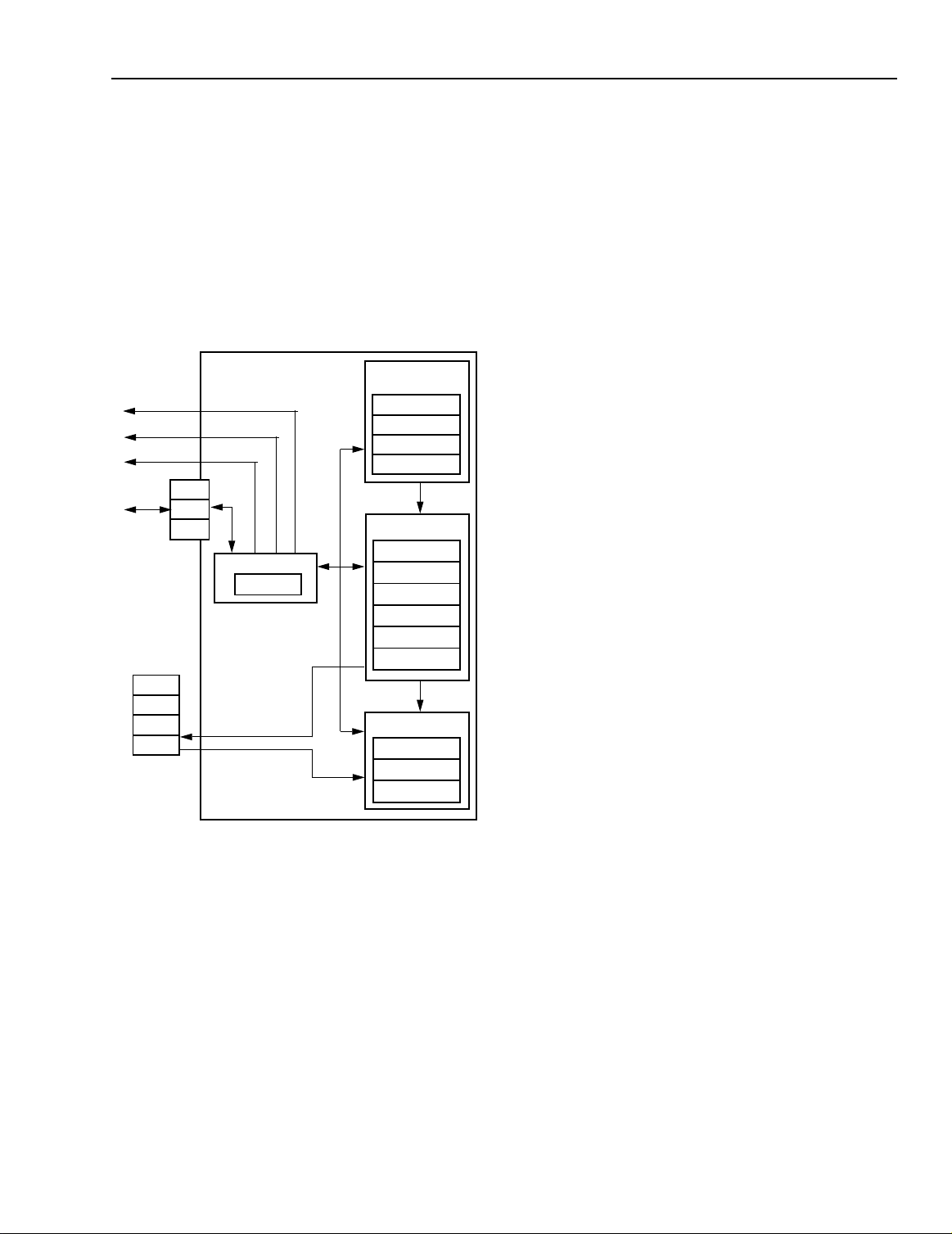
Preliminary Data Sheet
February 1997 DSP1628 Digital Signal Processor
4 Hardware Architecture (continued)
multaneous DSP-ECCP activity, however, ECCP internal edr registers as well as the shared bank of RAM,
In wideband low data rate applications, additive white
Gaussian noise (AWGN) is the principle channel impairment, and Euclidean branch metric computation for
convolutional decoding is selected by resetting the
branch metric select bit to zero.
A traceback-length register is provided for programming
the traceback decode length.
A block diagram of the coprocessor and its interface to
the DSP1600 core is shown in the following figure:
RAM4, are not accessible to the user's DSP code.
Branch Metric Unit: The branch metric unit of the
ECCP performs full-precision real and complex arithmetic for computing 16-bit incremental branch metrics
required for MLSE equalization and convolutional decoding.
MLSE Branch Metric Unit: To generate the estimated
received complex signal at instance n, E(n, k) = EI(n, k)
+ j EQ(n, k), at the receiver, all possible states, k = 0 to
2C – 1 – 1, taking part in the Viterbi state transition are
convolved with the estimated channel impulse response, H(n) = [h(n), h(n – 1), h(n – 2), . . . , h(n – C +
1)] T, where the constraint length C = {2 to 6}. Each inphase and quadrature-phase part of the channel tap,
h(n) = hI(n) + j hQ(n), is quantized to an 8-bit 2's complement number.
The channel estimates are normalized prior to loading
into the ECCP such that the worst-case summation of
the hI(n) or hQ(n) are confined within a 10-bit 2's complement number. The in-phase and quadrature-phase
parts of the received complex signal Z(n) = ZI(n) + j
ZQ(n) are also confined within a10-bit 2's complement
number. The Euclidean branch metric associated with
each of the 2C state transitions is calculated as:
BM(n, k) = XI(n, k)2 + XQ(n, k)2
where
XI(n, k) = abs{ZI(n) – EI(n, k)}
EOVF
EREADY
EBUSY
IDB
ear
edr
eir
CONTROL UNIT
ECON
ECCP
BRANCH METRIC
UNIT
SiHi, i = 0, . . . ,5
ZIG10
ZQG32
G54
UPDATE UNIT
NS[63:0]
PS[63:0]
SYC
MDX
MACH
MACL
and
XQ(n, k) = abs{ZQ(n) – EQ(n, k)}
RAM4
TRACEBACK UNIT
TBLR
DSR
TBSR
The absolute values of the difference signal are saturated at level 0xFF. The sixteen most significant bits of this
17-bit incremental branch metric are retained for the
add-compare-select operation of the Viterbi algorithm.
The in-phase and quadrature-phase parts of the re-
5-4500 (F)
ceived complex signal are stored in ZIG10 and ZQG32
registers, respectively. The complex estimated channel
taps H5 through H0 are stored in S5H5 through S0H0
Figure 7. Error Correction Coprocessor Block
Diagram/Programming Model
registers, such that the in-phase part of the channel occupies the upper byte and the quadrature-phase part of
the channel occupies the lower byte.
The ECCP internal registers are accessed indirectly
through the address and data registers, ear and edr.
The control register, ECON, and the traceback length
register, TBLR, are used to program the operating
mode of the ECCP. The symbol registers (S0H0—
S5H5, ZIG10, ZQG32), the generating polynomial registers (ZIG10, ZQG32, G54), and the channel impulse
registers (S0H0—S5H5) are used as input to the ECCP
for MLSE or convolutional decoding. Following a Viterbi
Convolutional Branch Metric Unit: Two types of distance
computation are implemented for convolutional decoding. Convolutional decoding over a Gaussian channel is
supported with Euclidean distance measure for rate 1/1
and 1/2 convolutional encoding. Convolutional decoding preceded by the MLSE equalization or other linear/
nonlinear equalization is supported with Manhattan distance measure for rate 1/1 through 1/6 convolutional
encoding.
decoding operation, the decoded symbol is read out of
the decoded symbol register, DSR. All internal states of
these memory-mapped registers are accessible and
controllable by the DSP program. During periods of siLucent Technologies Inc. 27

Preliminary Data Sheet
DSP1628 Digital Signal Processor February 1997
4 Hardware Architecture (continued)
Generating polynomials, G(0), . . . , G(5), up to six-delays corresponding to a constraint length of seven, may take
part in computing the estimated received signals, E(0, k), . . . , E(5, k), within the ECCP associated with all possible
state transitions, k = 0, 1, 2C – 1.
Six 8-bit soft symbols, S(0), . . . , S(5), are loaded into the ECCP. The incremental branch metrics associated with
all 2C state transitions are calculated as indicated in Table 10:
Table 10. Incremental Branch Metrics
Distance Measure Code Rate 16-bit Incremental Branch Metric
Euclidean 1/1
Euclidean 1/2
Manhattan 1/1 [S(i) – E(i)] << 8, i = 0
Manhattan 1/2 [(S(i) – E(i))] << 7, i = 0, 1
Manhattan 1/3 or 1/4 [(S(i) – E(i))] << 6, i = 0, 1, 2, or 3
Manhattan 1/5 or 1/6 [(S(i) – E(i))] << 5, i = 0, 1, . . . , 4 or 5
The received 8-bit signals S(5) through S(0) are stored in the S5H5 through S0H0 registers. The generating polynomials G(1) and G(0) are stored in the upper and lower bytes of the ZIG10 register, respectively. The generating
polynomials G(3) and G(2) are stored in the upper and lower bytes of the ZQG32 register, respectively. The generating polynomials G(5) and G(4) are stored in the upper and lower bytes of the G54 register, respectively.
Update Unit: The add-compare-select operation of the Viterbi algorithm is performed in this unit. At every time instant, there are 2C state transitions of which 2C – 1 state transitions survive. The update unit selects and updates
2C – 1 surviving sequences in the traceback RAM that consists of the 4th bank of the internal RAM, RAM4. The
accumulated cost of the path p at the Jth instant, ACC(J, p), is the sum of the incremental branch metrics belonging
to the path p up to the time instant J:
The update unit computes and stores full precision 24-bit resolution path metrics of the bit sequence. To assist the
detection of a near overflow in the accumulated path cost, an internal vectored interrupt, EOVF, is provided.
Traceback Unit: The traceback unit selects a path with the smallest path metric among 2C – 1 survivor paths at
every instant. The last signal of the path corresponding to the maximum likelihood sequence is delivered to the
decoder output. The depth of this last signal is programmable at the symbol rate. The traceback decoding starts
from the minimum cost index associated with the state with the minimum cost, min {Acc(j, p1), . . . , Acc(j, p2C – 1)}.
If the end state is known, the traceback decoding may be forced in the direction of the right path by writing the desired end state into the minimum cost index register, MIDX.
Interrupts and Flags: The ECCP interrupts the DSP1600 core when the ECCP has completed an instruction,
EREADY, or when an overflow in the accumulated cost is imminent, EOVF. Also, an EBUSY flag is provided to the
core to indicate when the ECCP is in operation.
Traceback RAM: The fourth 1 Kword bank of dual-port RAM is shared between the DSP1600 core and the ECCP.
RAM4, located in the Y memory space in the address range 0x0C00 to 0x0FFF, is used by the ECCP for storing
traceback information. When the ECCP is active, i.e., the EBUSY flag is asserted, the DSP core cannot access this
traceback RAM.
(S(0) – E(0))
[∑(S(i) – E(i))
ACC(J, p) = ∑BM(j, p), j = 1, . . . , J
2
2
] >> 1, i = 0, 1
28 Lucent Technologies Inc.
 Loading...