

AGERE DSP1627 Datasheet

Data Sheet
March 2000
DSP1627 Digital Signal Processor
1 Features
■ Optimized for digital cellular applications with a bit mani p-
ulation unit for higher coding efficiency.
■ On-chip, programmable, PLL clock synthesizer.
■ 14 ns and 11 ns instruction cycle times at 5 V, 10 ns in-
struction cycle time at 3.0 V, and 20 ns and 12.5 ns instruction cycle times at 2.7 V, respectively.
■ Mask-programmable memory map option: The
DSP1627x36 features 36 Kwords on-chip ROM. The
DSP1627x32 features 32 Kwords on-chip ROM and access to 16 Kwords external ROM in the same map. Both
feature 6 Kwords on-chip, dual-port RAM and a secure
option for on-chip ROM.
■ Low power consumption:
— <5.5 mW/MIPS typical at 5 V.
— <1.5 mW/MIPS typical at 2.7 V.
■ Flexible power management modes:
— Standard sleep: 0.5 mW/MIPS at 5 V.
0.12 mW/MIPS at 2.7 V.
— Sleep with slow internal clock: 1.4 mW at 5 V.
0.4 mW at 2.7 V.
— Hardware STOP (pin halts DSP): <20 µA.
■ Mask-programmable clock options: crystal oscillator,
small signal, and CMOS.
■ Low-profile TQFP package (1.5 mm) available.
■ Sequenced accesses to X and Y external memory.
■ Object code compatible with the DSP1617.
■ Single-cycle squaring.
■ 16 x 16-bit multiplication and 36-bit accumulation in one
instruction cycle.
■ Instruction cache for high-speed, program-efficient, zero-
overhead looping.
■ Dual 25 Mbits/s serial I/O ports with multiprocessor capa-
bility—16-bit data channel, 8-bit protocol channel.
■ 8-bit parallel host interface:
— Supports 8- or 16-bit transfers.
—
Motorola
■ 8-bit control I/O interface.
■ 256 memory-mapped I/O ports.
■
IEEE
*
Motorola
Intel
is a registered trademark of Intel Corp.
†
‡
IEEE
and Electronics Engineers, Inc.
*
or
‡
P1149.1 test port (JTAG boundary scan).
is a registered trademark of Motorola, Inc.
is a registered trademark of The Institute of Electrical
Intel
†
compatible.
■ Full-speed in-circuit emulation hardware development
system on-chip.
■ Supported by DSP1627 software and hardware develop-
ment tools.
2 Description
The DSP1627 is Lucent Technologies Microelectronics
Group first digital signal processor offering 100 MIPS operation at 3.0 V and 80 MIPS operation at 2.7 V with a reduction in power consumption. Designed specifically for
applications requiring low power dissipation in digital cellular systems, the DSP1627 is a signal-coding device that can
be programmed to perform a wide variety of fixed-point signal processing functions. The device is based on the
DSP1600 core with a bit manipulation unit for enhanced signal coding efficiency. The DSP1627 includes a mix of peripherals specifically intended to support processingintensive but cost-sensitive applications in the area of digital
wireless communications.
The DSP1627x36 contains 36 Kwords of internal ROM
(IROM), but it doesn’t support the use of IROM and external
ROM (EROM) in the same memory map. The DSP1627x32
supports the use of 32 Kwords of IROM with 16 Kwords of
EROM in the same map. Both devices contain 6 Kwords of
dual-port RAM (DPRAM), which allows simultaneous access to two RAM locations in a single instruction cycle.
The DSP1627 is object code compatible wi th the DSP1617,
while providing more memory and architectural enhancements including an on-chip clock synthesizer and an 8-bit
parallel host interface for hardware flexibility.
The DSP1627 supports 2.7 V, 3.0 V, and 5 V operation and
flexible power management modes required for portable
cellular terminals. Several control mechanis ms achieve lowpower operation, including a STOP pin for placing the DSP
into a fully static, halted state and a programmable power
control register used to power down unused on-chip I/O
units. These power management modes allow for trade-offs
between power reduction and wake-up latency requirements. During system standby, power consumption is reduced to less than 20 µA.
The on-chip clock synthesizer can be driv en by an external
clock whose frequency is a fraction of the instruction rate.
The device is packaged in a 100-pin BQFP or a 100-pin
TQFP and is available with 14 ns and 11 ns instruction cycle
times at 5 V, 10 ns instruction cycle times at 3.0 V, and
20 ns and 12.5 ns instruction cycle times at 2.7 V, respectively.

Data Sheet
DSP1627 Digital Signal Processor March 2000
Table of Contents
Contents Page Contents Page
1 Features.............................................................. 1
2 Description.......................................................... 1
3 Pin Information........................... ...... ....... ...... ...... 3
4 Hardware Architecture........................................ 7
4.1 DSP1627 Architectural Overview............. 7
4.2 DSP1600 Core Architectural Overview .. 10
4.3 Interrupts and Trap................................. 11
4.4 Memory Maps and Wait-States.............. 16
4.5 External Memory Interface (EMI)............ 18
4.6 Bit Manipulation Unit (BMU)................... 19
4.7 Serial I/O Units (SIOs)............................ 19
4.8 Parallel Host Interface (PHIF)................. 22
4.9 Bit Input/Output Unit (BIO)...................... 23
4.10 Timer ...................................................... 23
4.11 JTAG Test Port....................................... 24
4.12 Clock Synthesis...................................... 26
4.13 Power Management ............................... 29
5 Software Architecture ....................................... 36
5.1 Instruction Set......................................... 36
5.2 Register Settings .................................... 45
5.3 Instruction Set Formats .......................... 55
6 Signal Descriptions ........................................... 61
6.1 System Interface..................................... 61
6.2 External Memory Interface ..................... 63
6.3 Serial Interface #1 .................................. 64
6.4 Parallel Host Interface or Serial
Interface #2 and Control I/O Interface.... 65
6.5 Control I/O Interface ............................... 65
6.6 JTAG Test Interface ............................... 66
7 Mask-Programmable Options ........................... 67
7.1 Input Clock Options ................................ 67
7.2 Memory Map Options ............................. 67
7.3 ROM Security Options............................ 67
8 Device Characteristics ...................................... 68
8.1 Absolute Maximum Ratings.................... 68
8.2 Handling Precautions ............................. 68
8.3 Recommended Operating Conditions .... 68
8.4 Package Thermal Considerations .......... 69
9 Electrical Characteristics and Requirements .... 70
9.1 Power Dissipation................................... 73
10 Timing Characteristics for 5 V Operation.......... 75
10.1 DSP Clock Generation ........................... 76
10.2 Reset Circuit........................................... 77
10.3 Reset Synchronization............................ 78
10.4 JTAG I/O Specifications.......................... 79
10.5 Interrupt .................................................. 80
10.6 Bit Input/Output (BIO) ............................. 81
10.7 External Memory Interface...................... 82
10.8 PHIF Specifications ................................ 86
10.9 Serial I/O Specifications.......................... 92
10.10 Multiprocessor Communication .............. 97
11 Timing Characteristics for 3.0 V Operation ....... 98
11.1 DSP Clock Generation............................ 99
11.2 Reset Circuit......................................... 100
11.3 Reset Synchronization....... ...... ....... ...... 101
11.4 JTAG I/O Specifications........................ 102
11.5 Interrupt ................................................ 103
11.6 Bit Input/Output (BIO) ........................... 104
11.7 External Memory Interface.................... 105
11.8 PHIF Specifications .............................. 109
11.9 Serial I/O Specifications........................ 115
11.10 Multiprocessor Communication ............ 120
12 Timing Characteristics for 2.7 V Operation ..... 121
12.1 DSP Clock Generation.......................... 122
12.2 Reset Circuit......................................... 123
12.3 Reset Synchronization....... ...... ....... ...... 124
12.4 JTAG I/O Specifications........................ 125
12.5 Interrupt ................................................ 126
12.6 Bit Input/Output (BIO) ........................... 127
12.7 External Memory Interface.................... 128
12.8 PHIF Specifications .............................. 132
12.9 Serial I/O Specifications........................ 138
12.10 Multiprocessor Communication ............ 143
13 Crystal Electrical Characteristics and
Requirements.................................................. 144
13.1 External Components for the Crystal
Oscillator............................................... 144
13.2 Power Dissipation................................. 144
13.3 LC Network Design for Third
Overtone Crystal Circuits...................... 147
13.4 Frequency Accuracy Considerations.... 149
14 Outline Diagrams ............................................ 152
14.1 100-Pin BQFP (Bumpered Quad
Flat Pack).............................................. 152
14.2 100-Pin TQFP (Thin Quad Flat Pack)... 153
2 Lucent Technologies Inc.
Data Sheet
March 2000 DSP1627 Digital Signal Processor
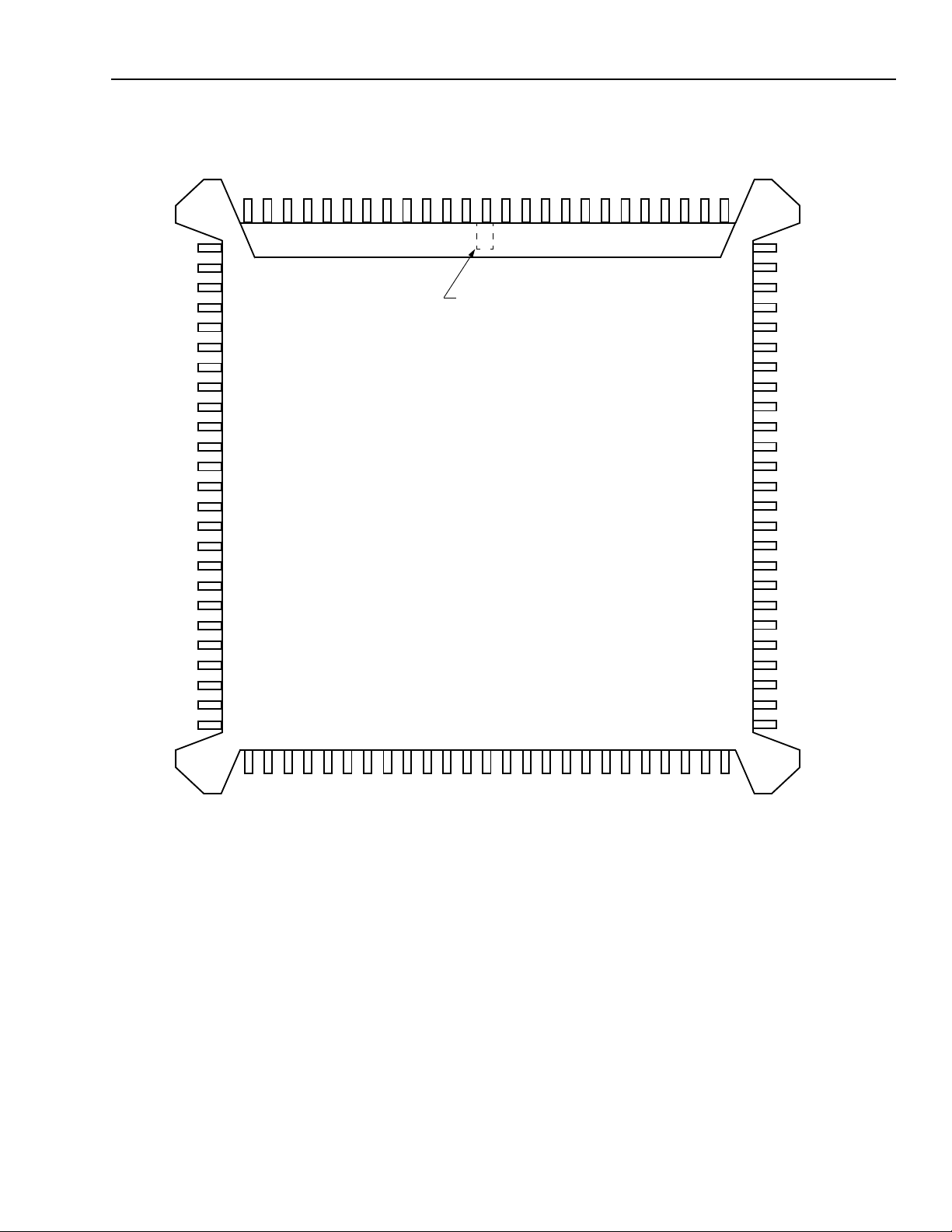
3 Pin Information
SS
V
DB4
DB3
DB2
DB1
DB0
IO
ERAMHI
DD
V
ERAMLO
EROM
RWN
SS
V
EXM
AB15
AB14
DD
V
AB13
AB12
AB11
AB10
AB9
AB8
AB7
SS
V
20
30
DD
V
DB5
40
DB6
V
SS
DB10
DB9
DB8
DB7
DB11
DB12
DB13
10
DB14
DB15
VDDIBF1
100
OBE1
SS
V
DI1
ILD1
OLD1
OCK1
ICK1
DO1
SYNC1
90
SS
V
DD
V
SADD1
DOEN1
PIN #1
IDENTIFIER
ZONE
OCK2/PCSN
DO2/PSTAT
SYNC2/PBSEL
ILD2/PIDS
OLD2/PODS
80
IBF2/PIBF
OBE2/POBE
ICK2/PB0
DI2/PB1
SS
DSP1627
V
DOEN2/PB2
SADD2/PB3
DD
V
IOBIT0/PB4
IOBIT1/PB5
70
IOBIT2/PB6
IOBIT3/PB7
VEC3/IOBIT4
VEC2/IOBIT5
VEC1/IOBIT6
VEC0/IOBIT7
SS
50
60
V
DD
V
SS
AB0
AB1
AB2
AB3
AB4
AB5
AB6
V
INT0
INT1
IACK
TRAP
STOP
DD
V
TCK
CKO
RSTB
TMS
TDO
DDA
TDI
V
CKI
CKI2
SSA
V
5-4218 (F).b
Figure 1. DSP1627 BQFP Pin Diagram
Lucent Technologies Inc. 3

Data Sheet
DSP1627 Digital Signal Processor March 2000
3 Pin Information
VDDDB5
SS
1
V
DB4
DB3
DB2
DB1
DB0
ERAMHI
V
ERAMLO
EROM
RWN
V
EXM
AB15
AB14
V
AB13
AB12
AB11
AB10
AB9
AB8
AB7
V
IO
DD
10
SS
DD
20
SS
100
(continued)
DB6
DB7
DB8
30
DO1
SYNC1
SS
V
DD
V
DB9
DB10
VSSDB11
DB12
DB13
DB14
DB15
VDDOBE1
IBF1
VSSDI1
ILD1
90
OLD1
ICK1
OCK1
80
SADD1
DOEN1
OCK2/PCSN
DO2/PSTAT
SYNC2/PBSEL
70
ILD2/PIDS
OLD2/PODS
IBF2/PIBF
OBE2/POBE
ICK2/PB0
DI2/PB1
SS
DSP1627
V
DOEN2/PB2
SADD2/PB3
DD
V
60
IOBIT0/PB4
IOBIT1/PB5
IOBIT2/PB6
IOBIT3/PB7
VEC3/IOBIT4
VEC2/IOBIT5
VEC1/IOBIT6
VEC0/IOBIT7
SS
40
50
V
DD
V
AB6
AB5
AB4
AB3
AB2
AB0
AB1
SS
V
INT1
INT0
IACK
STOP
TRAP
RSTB
DD
V
TCK
CKO
TMS
TDO
DDA
TDI
V
CKI
CKI2
SSA
V
5-4219 (F).b
Figure 2. DSP1627 TQFP Pin Diagram
4 Lucent Technologies Inc.
Data Sheet
March 2000 DSP1627 Digital Signal Processor
3 Pin Information
(continued)
Functional descriptions of pins 1—100 are found in Section 6, Signal Descriptions. The functionality of pins 61 and
62 (TQFP pins 48 and 49) are mask-programmable (see Section 7, Mask-Programmable Options). Input levels on
all I and I/O type pins are designed to remain at full CMOS levels when not driven by the DSP.
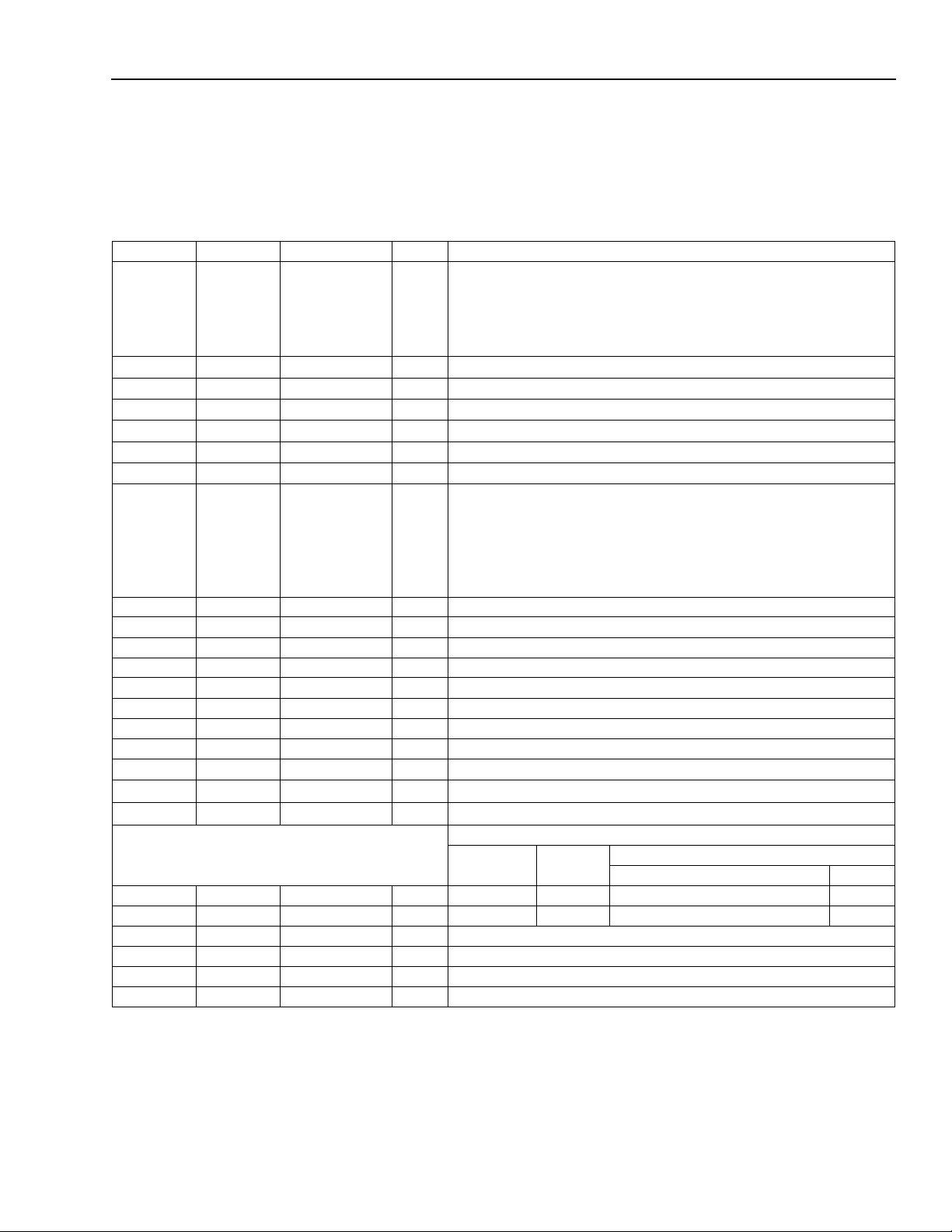
Table 1. Pin Descriptions
BQFP Pin TQFP Pin Symbol Type Name/Function
1, 2, 3, 4,
5, 7, 8, 9,
10, 11, 12,
15, 16, 17,
18, 19
88, 89, 90,
91, 92, 94,
95, 96, 97,
98, 99, 2,
3, 4, 5, 6
20 7 IO
21 8 ERAMHI
23 10 ERAMLO
24 11 EROM
25 12 RWN
DB[15:0] I/O* External Memory Data Bus DB[15:0].
†
Data Address 0x4000 to 0x40FF I/O Enable.
O
†
Data Address 0x8000 to 0xFFFF External RAM Enable.
O
†
Data Address 0x4100 to 0x7FFF External RAM Ena ble.
O
†
Program Address External ROM Enable.
O
†
Read/Write Not.
O
27 14 EXM I External ROM Enable.
28, 29, 31,
32, 33, 34,
35, 36, 37,
40, 41, 42,
43, 44, 45,
46
15, 16, 18,
19, 20, 21,
22, 23, 24,
27, 28, 29,
30, 31, 32,
33
AB[15:0] O* External Memory Address Bus 15—0.
47 34 INT1 I Vectored Interrupt 1.
48 35 INT0 I Vectored Interrupt 0.
50 37 IACK O* Interrupt Acknowledge.
51 38 STOP I STOP Inpu t Clock.
52 39 TRAP I/O* Nonmaskable Program Trap/Breakpoint Indication.
53 40 RSTB I Reset Bar.
54 41 CKO
†
Processor Clock Output.
O
56 43 TCK I JTAG Text Clock.
‡
57 44 TMS
58 45 TDO
59 46 TDI
JTAG Test Mode Select.
I
§
JTAG Test Data Output.
O
‡
JTAG Test Data Input.
I
Mask-Programmable Input Clock Option
CMOS Small
Signal
61 48 CKI** I CKI V
62 49 CKI2** I V
SSA
AC
V
CM
XLO, 10 pF capacitor to V
XHI, 10 pF capacitor to V
Crystal
Oscillator CMOS
CKI
SS
Open
SS
65 52 VEC0/IOBIT7 I/O* Vectored Interrupt Indication 0/Status/Control Bit 7.
66 53 VEC1/IOBIT6 I/O* Vectored Interrupt Indication 1/Status/Control Bit 6.
67 54 VEC2/IOBIT5 I/O* Vectored Interrupt Indication 2/Status/Control Bit 5.
68 55 VEC3/IOBIT4 I/O* Vectored Interrupt Indication 3/Status/Control Bit 4.
* 3-states when RSTB = 0, or by JTAG control.
† 3-states when RSTB = 0 and INT0 = 1. Output = 1 when RSTB = 0 and INT0 = 0, except CKO which is free-running.
‡ Pull-up devices on input.
§ 3-states by JTAG control.
** See Section 7, Mask-Programmable Options.
†† For SIO multiprocessor applications, add 5 kΩ external pull-up resistors to SADD1 and/or SADD2 for proper initialization.
Lucent Technologies Inc. 5

Data Sheet
DSP1627 Digital Signal Processor March 2000
3 Pin Information
(continued)
Functional descriptions of pins 1—100 are found in Section 6, Signal Descriptions.
Table 1. Pin Descriptions
(continued)
BQFP Pin TQFP Pin Symbol Type Name/Function
69 56 IOBIT3/PB7 I/O* Status/Control Bit 3/PHIF Data Bus Bit 7.
70 57 IOBIT2/PB6 I/O* Status/Control Bit 2/PHIF Data Bus Bit 6.
71 58 IOBIT1/PB5 I/O* Status/Control Bit 1/PHIF Data Bus Bit 5.
72 59 IOBIT0/PB4 I/O* Status/Control Bit 0/PHIF Data Bus Bit 4.
74 61
SADD2/PB3
††
I/O* SIO2 Multiprocessor Address/PHIF Data Bus Bit 3.
75 62 DOEN2/PB2 I/O* SIO2 Data Output Enable/PHIF Data Bus Bit 2.
77 64 DI2/PB1 I/O* SIO2 Data Input/PHIF Data Bus Bit 1.
78 65 ICK2/PB0 I/O* SIO2 Input Clock/PHIF Data Bus Bit 0.
79 66 OBE2/POBE O* SIO2 Output Buffer Empty/PHIF Output Buffer Empty.
80 67 IBF2/PIBF O* SIO2 Input Buffer Full/PHIF Input Buffer Full.
81 68 OLD2/PODS I/O* SIO2 Output Load/PHIF Output Data Strobe.
82 69 ILD2/PIDS I/O* SIO2 Input Load/PHIF Input Data Strobe.
83 70 SYNC2/PBSEL I/O* SIO2 Multiprocessor Synchronization/PHIF Byte Select.
84 71 DO2/PSTAT I/O* SIO2 Data Output/PHIF Status Register Select.
85 72 OCK2/PCSN I/O* SIO2 Output Clock/PHIF Chip Select Not.
86 73 DOEN1 I/O* SIO1 Data Output Enable.
87 74
SADD1
††
I/O* SIO1 Multiprocessor Address.
90 77 SYNC1 I/O* SIO1 Multiprocessor Synchronization.
91 78 DO1 O* SIO1 Data Output.
92 79 OLD1 I/O* SIO1 Output Load.
93 80 OCK1 I/O* SIO1 Output Clock.
94 81 ICK1 I/O* SIO1 Input Clock.
95 82 ILD1 I/O* SIO1 Input Load.
96 83 DI1 I SIO1 Data Input.
98 85 IBF1 O* SIO1 Input Buffer Full.
99 86 OBE1 O* SIO1 Output Buffer Empty.
6, 15, 26,
38, 49, 64,
76, 89, 97
14, 22, 30,
39, 55, 73,
88, 100
60 47 V
63 50 V
93, 1, 13,
25, 36, 51,
63, 76, 84
100, 9, 17,
26, 42, 60,
75, 87
V
V
DDA
SSA
SS
DD
P Ground.
P Power Supply.
P Analog Power Supply.
P Analog Ground.
* 3-states when RSTB = 0, or by JTAG control.
† 3-states when RSTB = 0 and INT0 = 1. Output = 1 when RSTB = 0 and INT0 = 0.
§ Pull-up devices on input.
‡ 3-states by JTAG control.
** See Section 7, Mask-Programmable Options.
†† For SIO multiprocessor applications, add 5 kΩ external pull-up resistors to SADD1 and/or SADD2 for proper initialization.
6 Lucent Technologies Inc.

Data Sheet
March 2000 DSP1627 Digital Signal Processor
4 Hardware Architecture
The DSP1627 device is a 16-bit, fixed-point programmable digital signal processor (DSP). The DSP1627
consists of a DSP1600 core to
ory and peripherals. Added architectural features give
the DSP1627 high program efficiency for signal coding
applications.
4.1 DSP1627 Architectural Overview
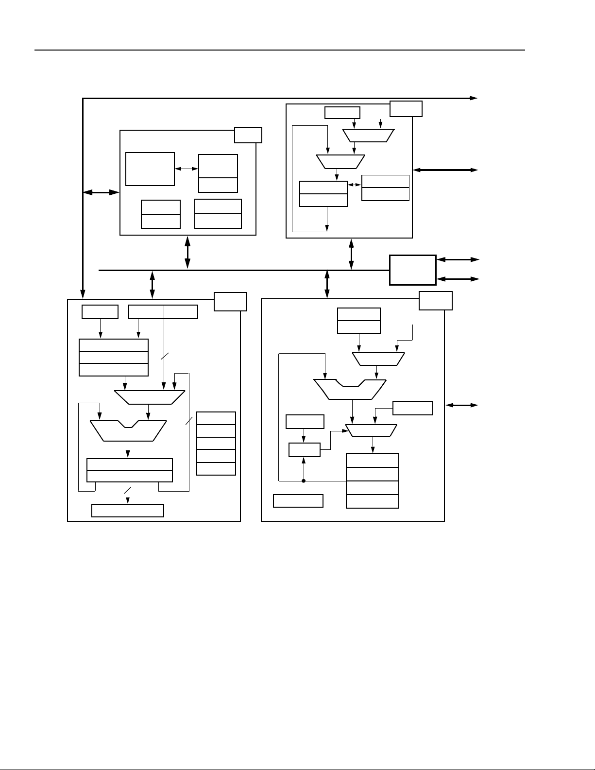
Figure 3 shows a block diagram of the DSP1627. The following modules make up t he D SP1627.
DSP1600 Core
The DSP1600 core is the heart of the DSP1627 chip. The
core contains data and address arithmetic units, an d
control for on-chip memory and peripherals. The core
provides support for external memory wait-states and onchip, dual-port RAM and features vectored interrupts and
a trap mechanism.
Dual-Port RAM (DPRAM)
This module contains six banks of zero wait-state memory. Each bank consists of 1K 16-bit words and has separate address and data ports to the instruction/coefficient
and data memory space s. A program can reference
memory from either space. The DSP1600 core automatically performs the required multiplexing. If references to
both ports of a single bank are made simultaneously, the
DSP1600 core automatically inserts a wait-state and performs the data port access first, followed by the instruction/coefficient port access.
A program can be downloaded from slow, off-chip memory into DPRAM, and then executed without wait-states.
DPRAM is also useful for improving convolution perf ormance in cases where the coefficients are adaptive.
Since DPRAM can be dow nloaded through the JTAG
port, full-speed remote in -c irc uit em ulation is possible.
DPRAM can also be used for downloading self-test code
via the JTAG port.
Read-Only Memory (ROM)
The DSP1627x36 contains 36K 16-bit words of zero
wait-state mask-progr am m able ROM for program and
fixed coefficients. Simila rly , the DS P1627x32 has 32K
16-bit words of ROM and acc es s to 16 Kw ords of external ROM.
External Memory Multiplexer (EMUX)
The EMUX is used to connec t the DS P1627 to external
memory and I/O devices. I t supports read/write opera tions from/to instruction/coefficient memory (X memory
space) and data memory (Y memory space). The
DSP1600 core automatically controls the EMUX. Instruc-
ether with on-chip mem-
g
tions can transparently refere nc e ex t ernal memory from
either set of internal buses. A sequencer allows a single
instruction to access both the X and the Y external memory spaces.
Clock Synthesis
The DSP powers up with a 1X input clock (CKI/CKI2) as
the source for the processor clock. An on-chip clock synthesizer (PLL) can also be used to generate the system
clock for the DSP, which will run at a freque nc y mu lti ple
of the input clock. The clock s y nt hes iz er is deselected
and powered down on reset. For low-power operation, an
internally generated slow clo c k can be used to drive the
DSP. If both the clock synthesizer and the internally generated slow clock are selec t ed, th e s low c loc k wi ll driv e
the DSP; however, the synt hesizer will continue to run.
The clock synthesizer and other programmable cloc k
sources are discussed in Section 4.12. The use of these
programmable clock so urc es f or power management is
discussed in Section 4.13.
Bit Manipulation Unit (BMU)
The BMU extends the DSP1600 core instruction set to
provide more efficient bit operations on accumula to rs .
The BMU contains logic for barrel shifting, normalization,
and bit field insertion/extraction. The unit also contains a
set of 36-bit alternate accu m ulators. The data in the alternate accumulators can be shuffled with the data in the
main accumulators. Flags returned by the BMU mesh
seamlessly with the DSP1600 conditional instructions.
Bit Input/Output (BIO)
The BIO provides conve nient and efficient monitorin g
and control of eight individually configurable pins. When
configured as outputs, th e pins can be individually set,
cleared, or toggled. When configured as inputs, individual pins or combinations of pins can be tested for patterns.
Flags returned by the BIO me s h se am lessly with conditional instructions.
Serial Input/Output Units (SIO and SIO2)
SIO and SIO2 offer asynchronous, full-duplex, do ublebuffered channels that operate at up to 25 Mbits/s (for
20 ns instruction cycle in a nonmultiprocessor configuration), and easily interface with other Lucent Technologies
fixed-point DSPs in a multiple-processor environm ent.
Commercially availab le c odecs and time-division mu lti plex (TDM) channels can be interfaced to the serial I/O
ports with few, if any, additional components. SIO2 is
identical to SIO.
An 8-bit serial protocol channel may be transmitted in addition to the address of the ca lled processor in multiprocessor mode. This feature is useful for transmitting highlevel framing informatio n or f or error detection and correction. SIO2 and BIO are pin-multiplexed with the PHIF.
Lucent Technologies Inc. 7

Data Sheet
DSP1627 Digital Signal Processor March 2000
4 Hardware Architecture
AB[15:0]DB[15:0]
ioc
DUAL-PORT
RAM
6K x 16
CKI
CKI2
CKO
RSTB
STOP
TRAP
INT[1:0]
IACK
VEC[3:0] OR IOBIT[7:4]
DO2 OR PSTAT
OLD2 OR PODS
OCK2 OR PCSN
OBE2 OR POBE
SYNC2 OR PBSEL
ICK2 OR PB0
ILD2 OR PIDS
DI2 OR PB1
IBF2 OR PIBF
DOEN2 OR PB2
SADD2 OR PB3
IO BIT[3:0] OR PB[7:4]
M
U
X
(continued)
RWN EXM EROM ERAMHI
EXTERNAL MEMORY INTERFACE & EMUX
YAB YDB XDB XAB BMU
DSP1600 CORE
PHIF
phifc
*
PSTAT
pdx0(IN)
pdx0(OUT)
I/O
IDB
powerc
BIO
sbit
cbit
36K/32K x 16
aa0
aa1
ar0
ar1
ar2
ar3
pllc
ERAMLO
ROM
†
SIO2
sdx2(OUT)
srta2
tdms2
sdx2(IN)
sioc2
saddx2
JTAG
BOUNDARY SCAN
jtag
*
JCON
*
ID
*
BYPASS
HDS
BREAKPOINT
TRACE
TIMER
timerc
timer0
sdx(OUT)
sdx(IN)
*
*
SIO
srta
tdms
sioc
saddx
*
TDO
TDI
TCK
TMS
TRST
DI1
ICK1
ILD1
IBF1
DO1
OCK1
OLD1
OBE1
SYNC1
SADD1
DOEN1
5-4142 (F).f
* These registers are accessible through the pins only.
† 36K x 16 for the DSP1627x36; 32K x 16 for the DSP1627x32.
Figure 3. DSP1627 Block Diagram
8 Lucent Technologies Inc.

Data Sheet
March 2000 DSP1627 Digital Signal Processor
4 Hardware Architecture
Table 2. DSP1627 Block Diagram Legend
Symbol Name
aa<0—1> Alternate Accumulators.
ar<0—3> Auxiliary BMU Registers.
BIO Bit Input/Output Unit.
BMU Bit Manipulation Unit .
BREAKPOINT Four Instruction Breakpoint Registers.
BYPASS JTAG Bypass Register.
cbit Control Register for BIO.
EMUX External Memory Multiplexer.
HDS Hardware Development System.
ID JTAG Device Identification Register.
IDB Internal Data Bus.
ioc I/O Configuration Register.
JCON JTAG Configuration Registers.
jtag 16-bit Serial/Parallel Register.
pdx0(in) Parallel Data Transmit Input Register 0.
pdx0(out) Parallel Data Transmit Output Register 0.
PHIF Parallel Host Interface.
phifc Parallel Host Interface Control Register.
pllc Phase-Locked Loop Control Register.
powerc Power Control Register.
PSTAT Parallel Host Interface Status Register.
ROM Internal ROM (36 Kwords for DSP1627x36, 32 Kwords for DSP1627x32).
saddx Multiprocessor Protocol Register.
saddx2 Multiprocessor Protocol Register for SIO2.
sbit Status Register for BIO.
sdx(in) Serial Data Transmit Input Register.
sdx2(in) Serial Data Transmit Input Register for SIO2.
sdx(out) Serial Data Transmit Output Register.
sdx2(out) Serial Data Transmit Output Register for SIO2.
SIO Serial Input/Output Unit.
SIO2 Serial Input/Output Unit #2.
sioc Serial I/O Control Register.
sioc2 Serial I/O Control Register for SIO2.
srta Serial Receive/Transmit Address Register.
srta2 Serial Receive/Transmit Address Register for SIO2.
tdms Serial I/O Time-division Multiplex Signal Control Register.
tdms2 Serial I/O Time-division Multiplex Signal Control Register for SIO2.
TIMER Programmab le Time r.
timer0 Timer Running Count Register.
timerc Timer Control Register.
TRACE Program Discontinuity Trace Buffer.
XAB Program Memory Address Bus.
XDB Program Memory Data Bus.
YAB Data Memory Address Bus.
YDB Data Memory Data Bus.
(continued)
Lucent Technologies Inc. 9

Data Sheet
DSP1627 Digital Signal Processor March 2000
4 Hardware Architecture
Parallel Host Interface (PHIF)
The PHIF is a passive, 8-bit parallel port which can interface to an 8-bit bus containing other Lucent Technologies DSPs (e.g., DSP1620, DSP1627, DSP1628,
DSP1629, DSP1611, DSP1616, DSP1617, DSP1618),
microprocessors, or peripheral I/O devices. The PHIF
port supports either
as 8-bit or 16-bit transfers, configured in software. The
port data rate depends upon the instruction cycle rate.
A 25 ns instruction cycle allows the PHIF to support
data rates up to 11.85 Mbytes/s, assuming the external
host device can transfer 1 byte of data in 25 ns.
The PHIF is accessed in two basic modes: 8-bit or
16-bit mode. In 16-bit mode, the host determines an access of the high or low byte. In 8-bit mode, only the low
byte is accessed. Software-programmable features allow for a glueless host interfac e to microprocessors
(see Section 4.8, Parallel Host Interface).
Timer
Motorola
or
Intel
(continued)
protocols, as well
In systems with multiple processors, the processors
may be configured such that any processor reaching a
breakpoint will cause all the other processors to be
trapped (see Section 4.3, Interrupts and Trap).
Pin Multiplexing
In order to allow flexible device interfacing while maintaining a low package pin count, the DSP1627 multiplexes 16 package pins between BIO, PHIF, VEC[3:0],
and SIO2.
Upon reset, the vectored interrupt indication signals,
VEC[3:0], are connected to the package pins while
IOBIT[4:7] are disconnected. Setting bit 12, EBIOH, of
the ioc register connects IOBIT[4:7] to the package pins
and disconnects VEC[3:0].
Upon reset, the parallel host interface (PHIF) is connected to the package pins while the second serial port
(SIO2) and IOBIT[3:0] are disconnected. Setting bit 10,
ESIO2, of the ioc register connects the SIO2 and
IOBIT[3:0] and disconnects the PHIF.
Power Management
The timer can be used to provide an interrupt at the expiration of a programmed interval. The interrupt may be
single or repetitive. More than nine orders of magnitude
of interval selection are provided. The timer may be
stopped and restarted at any time.
Hardware Development System (HDS) Module
The on-chip HDS performs instruction breakpointing
and branch tracing at full speed without additional offchip hardware. Using the JTAG port, the breakpointing
is set up, and the trace history is read back. The port
works in conjunction with the HDS code in the on-chip
ROM and the hardware and software in a remote computer. The HDS code must be linked to the user's application code and reside in the first 4 Kwords of ROM.
The on-chip HDS cannot be used with the secure ROM
masking option (see Section 7.3, ROM Security Options).
Four hardware breakpoints can be set on instruction addresses. A counter can be preset with the number of
breakpoints to receive before trapping the core. Breakpoints can be set in interrupt service routines. Alternately, the counter can be preset with the number of cache
instructions to execute before trapping the core.
Every time the program branches instead of executing
the next sequential instruction, the addresses of the instructions executed before and after the branch are
caught in circular memory. The memory contains the
last four pairs of program discontinuities for hardware
tracing.
Many applications, such as portable cellular terminals,
require programmable sleep modes for power management. There are three different control mechanisms for
achieving low-power operation: the powerc control register, the STOP pin, and the AWAIT bit in the alf register.
The AWAIT bit in the alf r egister al lows the pr ocessor to
go into a power-saving standby mode until an interrupt
occurs. The powerc register configures various powersaving modes by controlling internal clocks and peripheral I/O units. The STOP pin controls the internal processor clock. The various power management options
may be chosen based on power consumption and/or
wake-up latency requirements.
4.2 DSP1600 Core Architectural Overview
Figure 4 shows a block diagram of the DSP1600 core.
System Cache and Control Section (SYS)
This section of the core contains a 15-word cache memory and controls the instruction sequencing. It handles
vectored interrupts and traps, and also provides decoding for registers outside of the DSP1600 core. SYS
stretches the processor cycle if wait-states are required
(wait-states are programmable for external memory accesses). SYS sequences downloading via JTAG of selftest programs to on-chip, dual-port RAM.
The cache loop iteration count can be specified at run
time under program control as well as at assembly time.
10 Lucent Technologies Inc.

Data Sheet
March 2000 DSP1627 Digital Signal Processor
4 Hardware Architecture
Data Arithmetic Unit (DAU)
The data arithmetic unit (DAU) contains a 16 x 16-bit
parallel multiplier that generates a full 32-bit product in
one instruction cycle. The product can be accumulated
with one of two 36-bit accumulators. The accumulator
data can be directly loaded from, or stored to, memory
in two 16-bit words with optional saturation on overflow.
The arithmetic logic unit (ALU) supports a full set of
arithmetic and logical operations on either 16- or 32-bit
data. A standard set of flags can be tested for conditional ALU operations, branches, and subroutine calls. This
procedure allows the processor to perform as a powerful 16- or 32-bit microprocessor for logical and control
applications. The available instruction set is fully compatible with the DSP1617 instruction set. See Section
5.1 for more information on the instruction set.
The user also has access to two additional DAU regis-
ters. The psw register contains status information from
the DAU (see Table 26, Processor Status Word Register). The arithmetic control register, auc, is used to configure some of the features of the DAU (see Table 27)
including single-c ycle squar i ng. Th e auc regis ter alignment field supports an arithmetic shift left by one and
left or right by two. The auc register is cleared by reset.
The counters c0 to c2 are signed, 8 bits wide, and may
be used to count events such as the number of times
the program has executed a sequence of code. They
are controlled by the conditional instructions and provide a convenient method of program looping.
(continued)
The YAAU allows direct (or indexed) addressing of data
memory. In direct addressing, the 16-bit base register
(ybase) supplies the 11 most significant bits of the address. The direct data instruction supplies the remaining
5 bits to form an address to Y memory space and also
specifies one of 16 registers for the source or destination.
X Space Address Arithmetic Unit (XAAU)
The XAAU supports high-speed, register-indirect, instruction/coefficient memory addressing with postmodification of the register. The 16-bit pt register is used for
addressing coefficients. The signed register i holds a
user-defined postincrement. A fixed postincrement of
+1 is also available. Register PC is the program
counter. Registers pr and pi hold the return address for
subroutine calls and interrupts, respectively.
The XAAU decodes the 16-bit instruction/coefficient address and produces enable signals for the appropriate
X memory segment. The addressable X segments are
internal ROM (up to 36 Kwords for the DSP1627x36, up
to 32 Kwords for the DSP1627x32), six 1K banks of
DPRAM, and external ROM.
The locations of these memory segments depend upon
the memory map selected (see Table 5). A security
mode can be selected by mask option. This prevents
unauthorized access to the contents of on-chip ROM
(see Section 7, Mask-Programmable Options).
4.3 Interrupts and Trap
Y Space Address Arithmetic Unit (YAAU)
The YAAU supports high-speed, register-indirect, compound, and direct addressing of data (Y) memory. Four
general-purpose, 16-bit registers, r0 to r3, are available
in the YAAU. These registers can be used to supply the
read or write addresses for Y space data. The YAAU
also decodes the 16-bit data memory address and outputs individual memory enables for the data access.
The YAAU can address the six 1 Kword banks of onchip DPRAM or three external data memory segments.
Up to 48 Kwords of off-chip RAM are addressable, with
16K addresses reserved for internal RAM.
Two 16-bit registers, rb and re, allow zero-overhead
modulo addressing of data for efficient filter implementations. Two 16-bit signed registers, j and k, are used to
hold user-defined postmodification increments. Fixed
increments of +1, –1, and +2 are also available. Four
compound-addressing modes are provided to make
read/write operations more effi cient.
Lucent Technologies Inc. 11
The DSP1627 supports prioritized, vectored interrupts
and a trap. The device has eight internal hardware
sources of program interrupt and two external interrupt
pins. Additionally, there is a trap pin and a trap signal
from the hardware development system (HDS). A software interrupt is available through the
icall
The
Each of these sources of interrupt and trap has a unique
vector address and priority assigned to it. DSP16A interrupt compatibility is not maintained.
The software interrupt and the traps are always enabled
and do not have a corresponding bit in the ins register.
Other vectored interrupts are enabled in the inc register
(see Table 29, Interrupt Control (inc) Register) and
monitored in the ins register (see Table 30, Interrupt
Status (ins) Register). When the DSP1627 goes into an
interrupt or trap service routine, the IACK pin is asserted. In addition, pins VEC[3:0] encode which interrupt/
trap is being serviced. Table 4 details the encoding
used for VEC[3:0].
instruction is reserved for use by the HDS.
icall
instruction.
Data Sheet
DSP1627 Digital Signal Processor March 2000
4 Hardware Architecture
CONTROL
ins (16)
inc (16)
x (16)
16 x 16 MPY
SHIFT (–2, 0, 1, 2)
yh (16)
p (32)
yl (16)
32
(continued)
CACHE
cloop (7)
alf (16)
mwait (16)
DAU
SYS
ADDER
pc (16)
pt (16)
i (16)
MUX
j (16)
k (16)
1
pr (16)
pi (16)
MUX
XAAU
BRIDGE
–1, 0, 1, 2
XDB
XAB
IDB
YDB
YAAU
MUX
ALU/SHIFT
a0 (36)
a1 (36)
16
EXTRACT/SAT
c0 (8)
36
c1 (8)
c2 (8)
auc (16)
psw (16)
re (16)
CMP
ybase (16)
Figure 4. DSP1600 Core Block Diagram
ADDER
YAB
rb (16)
MUX
r0 (16)
r1 (16)
r2 (16)
r3 (16)
5-1741 (F).b
12 Lucent Technologies Inc.

Data Sheet
March 2000 DSP1627 Digital Signal Processor
4 Hardware Architecture
Table 3. DSP1600 Core Block Diagram Legend
Symbol Name
16 x 16 MPY 16-bit x 16-bit Multiplier.
a0—a1
alf AWAIT, LOWPR, Flags.
ALU/SHIFT Arithmetic Logic Unit/Shifter.
auc Arithmetic Unit Control.
c0—c2 Counters 0—2.
cloop Cache Loop Count.
CMP Comparator.
DAU Digital Arithmetic Unit.
i Increment Register for the X Address Space.
IDB Internal Data Bus.
inc Interrupt Control.
ins Interrupt Status.
j Increment Register for the Y Address Space.
k Increment Register for the Y Address Space.
MUX Multiplexer.
mwait External Memory Wait-states Register.
p Product Register (16-bit halves specified as p, pl).
PC Program Counter.
pi Program Interrupt Return Register.
pr Program Return Register.
psw Processor Status Word.
pt X Address Space Pointer.
r0—r3 Y Address Space Pointers.
rb Modulo Addressing Register (begin address ).
re Modulo Addressing Register (end addres s).
SYS System Cache and Control Section.
x Multiplier Input Register.
XAAU X Space Address Arithmetic Unit.
XAB X Space Address Bus.
XDB X Space Data Bus.
YAAU Y Space Address Arithmetic Unit.
YAB Y Space Address Bus.
YDB Y Space Data Bus.
ybase Direct Addressing Base Register.
y DAU Register (16-bit halves sp ec ifi ed as y, yl ).
* F3 ALU instructions with immediates require specifying the high half of the accumulators as a0h and a1h.
Accumulators 0 and 1 (16-bit halves specified as a0, a0l, a1, and a1l)
(continued)
*
.
Lucent Technologies Inc. 13

Data Sheet
DSP1627 Digital Signal Processor March 2000
4 Hardware Architecture
Interruptibility
Vectored interrupts are serviced only after the execution
of an interruptible instruction. If more than one vectored
interrupt is asserted at the same time, the interrupts are
serviced sequentially according to their assigned priorities. See Table 4 for the priorities assigned to the vectored interrupts. Interrupt service routines, branch and
conditional branch instructions, cache loops, and instructions that only decrement one of the RAM pointers,
r0 to r3 (e.g., *r3
A trap is similar to an interrupt, but it gains control of the
processor by branching to the trap service routine even
when the current instruction is noninterruptible. It may
not be possible to return to normal instruction execution
from the trap service routine since the machine state
cannot always be saved. In particular, program execution cannot be continued from a trapped cache loop or
interrupt service routine. While in a trap service routine,
another trap is ignored.
When set to 1, the status bits in the ins register indicate
that an interrupt has occurred. The processor must
reach an interruptible state (completion of an interruptible instruction) before an enabled vectored interrupt will
be acted on. An interrupt will not be serviced if it is not
enabled. Polled interrupt service can be implemented
by disabling the interrupt in the inc register and then
polling the ins register for the expected event.
Vectored Interrupts
Tables 29 and 30 show the inc and ins registers. A logic
1 written to any bit of inc enables (or unmasks) the associated interrupt. If the bit is cleared to a logic 0, the interrupt is masked. Note that neither the software
interrup t nor traps can be masked.
The occurrence of an interrupt that is not masked will
cause the program execution to transfer to the memory
location pointed to by that interrupt's vector address, assuming no other interrupt is being serviced (see Table
4, Interrupt Vector Table). The occurrence of an interrupt that is masked causes no automatic processor action, but will set the corresponding status bit in the ins
register. If a masked interrupt occurs, it is latched in the
ins register, but the interrupt is not taken. When unlatched, this latched interrupt will initiate automatic processor interrupt action. See the
Digital Signal Processor Information Manual
detailed description of the interrupts.
− −
), are not interruptible.
(continued)
DSP1611/17/18/27
for a more
Signaling Interrupt Service Status
Five pins of DSP1627 are devoted to signaling interrupt
service status. The IACK pin goes high while any interrupt or user trap is being serviced, and goes low when
the iretur n instruct ion fr om the se rvice ro utine is issued.
Four pins, VEC[3:0], carry a code indicating which of the
interrupts or trap is being serviced. Table 4 contains the
encodings used by each interrupt.
Traps due to HDS breakpoints have no effect on either
the IACK or VEC[3:0] pins. Instead, they show the interrupt state or interrupt source of the DSP when the trap
occurred.
Clearing Interrupts
The PHIF interrupts (PIBF and POBE) are cleared by
reading or writing the parallel host interface data transmit registers pdx0[in] and pdx0[out], respectively. The
SIO and SIO2 interrupts (IBF, IBF2, OBE, and OBE 2)
are cleared by reading or writing, as appropriate, the serial data registers sdx[in], sdx2[in], sdx[out], and
sdx2[out]. The JTAG interrupt (JINT) is cleared by reading the jtag register.
Three of the vectored interrupts are cleared by writing to
the ins register. Writing a 1 to the INT0, INT1, or TIME
bits in the ins will cause the corresponding interrupt status bit to be cleared to a logic 0. The status bit for these
vectored interrupts is also cleared when the ireturn instruction is executed, leaving set any other vectored interrupts that are pending.
Traps
The TRAP pin of the DSP1627 is a bidirectional signal.
At reset, it is configured as an input to the processor.
Asserting the TRAP pin will force a user trap. The trap
mechanism is used for two purposes. It can be used by
an application to rapidly gain control of the processor for
asynchronous tim e-cr it ical event hand li ng (typi c all y for
catastrophic error recovery). It is also used by the HDS
for breakpointing and gaining control of the processor.
Separate vectors are provided for the user trap (0x46)
and the HDS trap (0x3). Traps are not maskable.
14 Lucent Technologies Inc.

Data Sheet
March 2000 DSP1627 Digital Signal Processor
4 Hardware Architecture
Table 4. Interrupt Vector Table
Source Vector Priority VEC[3:0] Issued by
No Interrupt — — 0x0 —
Software Interrupt 0x2 1 0x1 icall
INT0 0x1 2 0x2 pin
JINT 0x42 3 0x8 jtag in
INT1 0x4 4 0x9 pin
TIME 0x10 7 0xc timer
IBF2 0x14 8 0xd SIO2 in
OBE2 0x18 9 0xe SIO2 out
Reserved 0x1c 10 0x0 —
Reserved 0x20 11 0x1 —
Reserved 0x24 12 0x2 —
IBF 0x2c 14 0x3 SIO in
OBE 0x30 15 0x4 SIO out
PIBF 0x34 16 0x5 PHIF in
POBE 0x38 17 0x6 PHIF out
TRAP from HDS 0x3 18
TRAP from User 0x46 19 = highest 0x7 pin
* Traps due to HDS breakpoints have no effect on VEC[3:0] pins.
(continued)
—
*
breakpoint, jtag, or pin
A trap has four cycles of latency. At most, two instructions will execute from the time the trap is received at
the pin to when it gains control. An instruction that is executing when a trap occurs is allowed to complete before the trap service routine is entered. (Note that the
instruction could be lengthened by wait-states.) During
normal program execution, the pi register contains either the address of the next instruction (two-cycle instruction executing) or the address following the next
instruction (one-cycle instruction executing). In an interrupt service routine, pi contains the interrupt return address. When a trap occurs during an interrupt service
routine, the value of the pi register may be overwritten.
Specifically, it is not possible to return to an interrupt
service routine from a user trap (0x46) service routine.
Continuing program execution when a trap occurs du ring a cache loop is also not possible.
The HDS trap causes circuitry to force the program
memory map to MA P1 (with on-chi p ROM starting at address 0x0) when the trap is taken. The previous memory map is restored when the trap service routine exits by
issuing an ireturn. The map is forced to MAP1 because
the HDS code, if present, resides in the on-chip ROM.
Using the Lucent Technologies development tools, the
TRAP pin may be configured to be an output, or an input
vectoring to address 0x3. In a multiprocessor environment, the TRAP pins of all the DSPs present can be tied
together. During HDS operations, one DSP is selected
by the host software to be the master. The master processor's TRAP pin is configured to be an output.
The TRAP pins of the slave processors are configured
as inputs. When the master processor reaches a breakpoint, the master's TRAP pin is asserted. The slave processors will respond to their TRAP input by beginning to
execute the HDS code.
AWAIT Interrupt (Standby or Sleep Mode)
Setting the AWAIT bit (bit 15) of the alf register
(alf = 0x8000) caus es th e proc esso r to go in to a po wer saving standby or sleep mode. Only the minimum circuitry on the chip required to process an incoming interrupt remains active. After the AWAIT bit is set, one
additional instruction will be executed before the standby power-s av in g m ode is ent e re d. A PH IF or SI O w or d
transfer will complete if already in progress. The AWAIT
bit is reset when the first interrupt occurs. The chip then
wakes up and continues executing.
nop
Two
AWAIT bit is set. The first
cuted before sleeping; the second will be executed after
the interrupt signal awakens the DSP and before the interrupt service routine is executed.
The AWAIT bit should be set from within the cache if the
code which is executing resides in external ROM where
more than one wait-state has been programmed. This
ensures that an interrupt will not disturb the device from
completely entering the sleep state.
instructions should be programmed after the
nop
(one cycle) will be exe-
Lucent Technologies Inc. 15

Data Sheet
DSP1627 Digital Signal Processor March 2000
4 Hardware Architecture
For additional power savings, set ioc = 0x0180 and timerc = 0x0040 in addition to setting alf = 0x8000. This will
hold the CKO pin low and shut down the timer and prescaler (see Table 38 and Table 31).
For a description of the control mechanisms for putting
the DSP into low-power modes, see Section 4.13, Power Management.
(continued)
4.4 Memory Maps and Wait-States
The DSP1600 core implements a modified Harvard architecture that has separate on-chip 16-bit address and
data buses for the instruction/coefficient (X) and data
(Y) memory spaces. Table 5 shows the instruction/coefficient memory space maps for both the DSP1627x36
and DSP1627x32.
The differences between the x36 and x32 memory
maps can be seen by comparing the respective MAP1
and MAP3. For instance, MAP1 of the x36 provides for
36 Kwords of IROM and 6 Kwords of dual-port RAM
(DPRAM), whereas MAP1 of the x32 provides for
32 Kwords of IROM, 6 Kwords of DPRAM, and
16 Kwords of EROM.
The DSP1627 provides a multiplexed external bus
which accesses external RAM (ERAM) and ROM (EROM). Programmable wait-states are provided for external memory accesses. The instruction/coefficient
memory map is configurable to provide application flexibility. Table 6 shows the data memory space, which
has one map.
Instruction/Coefficient Memory Map Selection
In determining which memory map to use, the processor evaluates the state of two parameters. The first is
the LOWPR bit (bit 14) of the alf register. The LOWPR
bit of the alf register is initialized to 0 automatically at reset. LOWPR controls the starting address in memory
assigned to the six 1K banks of dual-port RAM. If LOWPR is low, internal dual-port RAM begins at address
0xC000. If LOWPR is high, internal dual-port RAM begins at address 0x0. LOWPR also moves IROM from
0x0 in MAP1 to 0x4000 in MAP3, and EROM from 0x0
in MAP2 to 0x4000 in MAP4.
The second parameter is the value at reset of the EXM
pin (pin 27 or pin 14, depending upon the package
type). EXM determines whether the internal 36 Kwords
ROM (IROM) will be addressable in the memory map.
The Lucent Technologies development system tools,
together with the on-chip HDS circuitry and the JTAG
port, can independently set the memory map. Specifically, during an HDS trap, the memory map is forced to
16 Lucent Technologies Inc.
MAP1. The user's map selection is restored when the
trap service routine has completed execution.
MAP1
MAP1 has the IROM starting at 0x0 and six 1 Kword
banks of DPRAM starting at 0xC000. Additionally,
MAP1 for the x32 has 16 Kwords of EROM starting at
0x8000. MAP1 is used if DSP1627 has EXM low at reset and the LOWPR parameter is programmed to zero.
It is also used during an HDS trap.
MAP2
MAP2 differs from MAP1 in that the lowest 48 Kwords
referenc e extern al ROM (ERO M). MAP2 i s used if EX M
is high at reset, the LOWPR parameter is programmed
to zero, and an HDS trap is not in progress.
MAP3
MAP3 has the six 1 Kword banks of DPRAM starting at
address 0x0. In MAP3 of the x36, the 36 Kwords of
IROM start at 0x4000. Similarly, for the x32, 32 Kwords
of IROM start at 0x4000. Additionally, MAP3 for the x32
has 16 Kwords of EROM starting at 0xC000. MAP3 is
used if EXM is low at reset, the LOWPR bit is programmed to 1, and an HDS trap is not in progress. Note
that this map is not available if the secure mask-programmable option has been ordered.
MAP4
MAP4 differs from MAP3 in that addresses above
0x4000 reference external ROM (EROM). This map is
used if the LOWPR bit is programmed to 1, an HDS trap
is not in progress, and, either EXM is high during reset,
or the secure mask-programmable option has been ordered.
Whenever the chip is reset using the RSTB pin, the default memory map will be MAP1 or MAP2, depending
upon the state of the EXM pin at reset. A reset through
the HDS will not reinitialize the alf register, so the previous memory map is retained.
Boot from External ROM
After RSTB goes from low to high, the DSP1627 comes
out of reset and fetches an instruction from address
zero of the inst ruction/coefficient space. The physical
location of address zero is determined by the memory
map in effect. If EXM is high at the rising edge of RSTB,
MAP2 is selected. MAP2 has EROM at location zero;
thus, program execution begins from external memory.
If EXM is high and INT1 is low when RSTB rises, the
mwait register defaults to 15 wait-states for all external
memory segments. If INT1 is high, the mwait register
defaults to 0 wait-states.
Data Sheet
March 2000 DSP1627 Digital Signal Processor
4 Hardware Architecture
(continued)
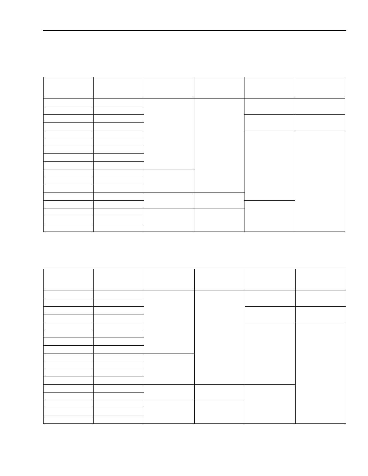
Table 5. Instruction/Coefficient Memory Maps
DSP1627x36
X Address AB[0:15] MAP 1
EXM = 0
LOWPR = 0
00x0000
4K 0x1000
IROM
(36K)
*
†
MAP 2
EXM = 1
LOWPR = 0
EROM
(48K)
LOWPR = 1
DPRAM
6K 0x1800 Reserved
12K 0x3000
MAP 3
EXM = 0
(6K)
(10K)
‡
LOWPR = 1
Reserved
16K 0x4000 IROM
20K 0x5000
(36K)
24K 0x6000
28K 0x7000
32K 0x8000
36K 0x9000 Reserved
40K 0xA000
(12K)
44K 0xB000
48K 0xC000 DPRAM
52K 0xD000 Reserved
(6K)
54K 0xD800 Reserved
56K 0xE000
(10K)
DPRAM
(6K)
Reserved
(10K)
(12K)
60K—64K 0xFFFF
* MAP1 is set automatically during an HDS trap. The user-selected map is restored at the end of the HDS trap service routine.
† LOWPR is an alf register bit. The Lucent Technologies development system tools can independently set the memory map.
‡ MAP3 is not available if the secure mask-programmable option is selected.
MAP 4
EXM = 1
DPRAM
(6K)
(10K)
EROM
(48K)
DSP1627x32
X Address AB[0:15] MAP 1
EXM = 0
LOWPR = 0
0 0x0000
4K 0x1000
IROM
(32K)
*
†
MAP 2
EXM = 1
LOWPR = 0
EROM
(48K)
LOWPR = 1
6K 0x1800 Reserved
12K 0x3000
DPRAM
MAP 3
EXM = 0
(6K)
(10K)
‡
LOWPR = 1
Reserved
16K 0x4000 IROM
20K 0x5000
(32K)
24K 0x6000
28K 0x7000
32K 0x8000 EROM
36K 0x9000
(16K)
40K 0xA000
44K 0xB000
48K 0xC000 DPRAM
52K 0xD000
(6K)
54K 0xD800 Reserved
56K 0xE000
(10K)
DPRAM
(6K)
Reserved
(10K)
EROM
(16K)
60K—64K 0xFFFF
* MAP1 is set automatically during an HDS trap. The user-selected map is restored at the end of the HDS trap service routine.
† LOWPR is an alf register bit. The Lucent Technologies development system tools can independently set the memory map.
‡ MAP3 is not available if the secure mask-programmable option is selected.
MAP 4
EXM = 1
DPRAM
(6K)
(10K)
EROM
(48K)
Lucent Technologies Inc. 17

Data Sheet
DSP1627 Digital Signal Processor March 2000
4 Hardware Architecture
Data Memory Mapping
Table 6. Data Memory Map (Not to Scale)
Decimal
Address
0 0x0000 DPRAM[1:6]
6K 0x1800 Reserved
16K 0x4000 IO
Address in
r0, r1, r2, r3
(continued)
Segment
4.5 External Memory Interface (EMI)
The external memory interface supports read/write operations from instruction/coefficient memory, data
memory, and memory-mapped I/O devices. The
DSP1627 provides a 16-bit external address bus,
AB[15:0], and a 16-bit external data bus, DB[15:0].
These buses are multiplexed between the internal buses for the instruction/coefficient memory and the data
memory. Four external memory segment enables,
ERAMLO, IO, ERAMHI, and EROM, select the external
memory segment to be addressed.
If a data memory location with an address between
0x4100 and 0x7FFF is addressed, ERAMLO is asserted
low.
(10K)
If one of the 256 external data memory locations, with
an address greater than or equal to 0x4000, and less
than or equal to 0x40FF, is addressed, IO is asserted
low. IO is intended for memory-mapped I/O.
If a data memory location with an address greater than
or equal to 0x8000 is addressed, ERAMHI is asserted
low. When the external instruction/coefficient memory is
addressed, EROM is asserted low.
16,640 0x4100 E RA MLO
32K 0x8000 ERAMHI
64K – 1 0xFFFF
On the data memory side (see Table 6), the six 1K
banks of dual-port RAM are located starting at address
0. Addresses from 0x4000 to 0x40FF reference a 256word memory-mapped I/O segment (IO). Addresses
from 0x4100 to 0x7FFF reference the low external data
RAM segment (ERAMLO). Addresses above 0x8000
reference high external data RAM (ERAMHI).
Wait-States
The number of wait-states (from 0 to 15) used when accessing each of the four external memory segments
(ERAMLO, IO, ERAMHI, and EROM) is programmable
in the mwait register (see Table 36). When the program
references memory in one of the four external segments, the internal multiplexer is automatically switched
to the appropriate set of internal buses, and the associated external enable of ERAMLO, IO, ERAMHI, or
EROM is issued. The external memory cycle is automatically stretched by the number of wait-states configured in the appropriate field of the mwait register.
The flexibility provided by the programmable options of
the external memory interface (see Table 36, mwait
Register and Table 38, ioc Register) allows the
DSP1627 to interface g luelessly with a variety of commercial memory chips.
Each of the four external memory segments, ERAMLO,
IO, ERAMHI, and EROM, has a number of wait-states
that is programmable (from 0 to 15) by writing to the
mwait register. When the program references memory
in one of the four external segments, the internal multiplexer is automatically switched to the appropriate set of
internal buses, and the associated external enable of
ERAMLO, IO, ERAMHI, or EROM is issued. The external memory cycle is automatically stretched by the number of wait-states in the appropriate field of the mwait
register.
When writing to external memory, the RWN pin goes
low for the external cycle. The external data bus,
DB[15:0], is driven by the DSP1627 starting halfway
through the cycle. The data driven on the external data
bus is automatically held after the cycle unless an external read cycle immediately follows.
The DSP1627 has one external address bus and one
external data bus for both memory spaces. Since some
instructions provide the capability of simultaneous access to both X space and Y space, some provision must
be made to avoid collisions for external accesses. The
DSP1627 has a sequencer that does the external X access first, and then the external Y access, transparently
to the programmer. Wait-states are maintained as
18 Lucent Technologies Inc.

Data Sheet
March 2000 DSP1627 Digital Signal Processor
4 Hardware Architecture
programmed in the mwait register. For example, let two
instructions be executed: the first reads a coefficient
from EROM and writes data to ERAM; the second reads
a coefficient from EROM and reads data from ERAM.
The sequencer carries out the following steps at the external memory interface: read EROM, write ERAM, read
EROM, and read ERAM. Each step is done in sequential one-instruction cycle steps, assuming zero waitstates are programmed. Note that the number of instruction cy cles taken by th e two in str uct ions is four . Also, in this case, the write hold time is zero.
The DSP1627 allows writing into external instruction/
coefficient memory. By setting bit 11, WEROM, of the
ioc register (see Table 38), writing to (or reading from)
data memory or memory-mapped I/O asserts the
EROM strobe instead of ERAMLO, IO, or ERAMHI.
Therefore, with WEROM set, EROM appears in both Y
space (replacing ERAM) and X space, in its normal position.
Bit 14 of the ioc register (see Table 38), EXTROM, may
be used with WEROM to download to a full 64K of external memory. When WEROM and EXTROM are both
asserted, address bit 15 (AB15) is held low, aliasing the
upper 32K of external memory into the lower 32K.
When an access to internal memory is made, the
AB[15:0] bus holds the last valid external memory address. Asserting the RSTB pin low 3-states the AB[15:0]
bus. After reset, the AB[15:0] value is undefined.
(continued)
4.6 Bit Manipulation Unit (BMU)
The BMU interfaces directly to the main accumulators in
the DAU providing the following features:
■
Barrel shifting—logical and arithmetic, left and right
shift
■
Normalization and extraction of exponent
■
Bit-field extraction and insertion
These features increase the efficiency of the DSP in applications such as control or data encoding and decoding. For example, data packing and unpacking, in which
short data words are packed into one 16-bit word for
more efficient memory storage, is very easy.
In addition, the BMU provides two auxiliary accumulators, aa0 and aa1. In one instruction cycle, 36-bit data
can be shuffled, or swapped, between one of the main
accumulators and one of the alternate accumulators.
The ar<0—3> registers are 16-bit registers that control
the operations of the BMU. They store a value that determines the amount of shift or the width and offset
fields for bit extraction or insertion. Certain operations in
the BMU set flags in the DAU psw register and the alf
register (see Table 26, Processor Status Word (psw)
Register, and Table 35, alf Register). The ar<0—3> registers can also be used as general-purpose registers.
The BMU instructions are detailed in Section 5.1. For a
thorough description of the BMU, see the
18/27 Digital Signal Processor Information Manual
DSP1611/17/
.
The leading edge of the memory segment enables can
be delayed by approximately one-half a CKO period by
programming the ioc register (see Table 38). This is
used to avoid a situation in which two devices drive the
data bus simultaneously.
Bits 7, 8, and 13 of the ioc register select the mode of
operation for the CKO pin (see Table 38). Available options are a free-running unstretched clock, a wait-stated
sequenced clock (runs through two complete cycles
during a sequenced external memory access), and a
wait-stated clock based on the internal instruction cycle.
These clocks drop to the low-speed internal ring oscillator when SLOWCKI is enabled (see 4.13, Power Management). The high-to-low transitions of the wait-stated
clock are synchronized to the high-to-low transition of
the free-running clock. Also, the CKO pin provides either a continuously high level, a continuously low level,
or changes at the rate of the internal processor clock.
This last option, only available with the crystal and
small-signal input clock options, enables the DSP1627
CKI input buffer to deliver a full-rate clock to other devices while the DSP1627 itself is in one of the low-power
modes.
4.7 Serial I/O Units (SIOs)
The serial I/O ports on the DSP1627 device provide a
serial interface to many codecs and signal processors
with little, if any, external hardware required. Each highspeed, double-buffered port (sdx and sdx2) supports
back-to-back transmissions of data. SIO and SIO2 are
identical. The output buffer empty (OBE and OBE2) and
input buffer full (IBF and IBF2) flags facilitate the reading and/or writing of each serial I/O port by programor interrupt-driven I/O. There are four selectable active
clock speeds.
A bit-reversal mode provi des comp atib ility with either
the most significant bit (MSB) first or least significant bit
(LSB) first serial I/O formats (see Table 22, Serial I/O
Control Registers (sioc and sioc2)). A multiprocessor
I/O configuration is supported. This feature allows up to
eight DSP161X devices to be connected together on an
SIO port without requiring external glue logic.
Lucent Technologies Inc. 19

Data Sheet
DSP1627 Digital Signal Processor March 2000
4 Hardware Architecture
The serial data may be internally looped back by setting
the SIO loopback control bit, SIOLBC, of the ioc register. SIOLBC affects both the SIO and SIO2. The data
output signals are wrapped around internally from the
output to the input (DO1 to DI1 and DO2 to DI2). To exercise loopback, the SIO clocks (ICK1, ICK2, OCK1,
and OCK2) should either all be in the active mode,
16-bit condition, or each pair should be driven from one
external source in passive mode. Similarly, pins ILD1
(ILD2) and OLD1 (OLD2) must both be in active mode
or tied together and driven from one external frame
clock in passive mode. During loopback, DO1, DO2,
DI1, DI2, ICK1, ICK2, OCK1, OCK2, ILD1, ILD2, OLD1,
OLD2, SADD1, SADD2, SYNC1, SYNC2, DOEN1, and
DOEN2 are 3-stated.
Setting DODLY = 1 (sioc and sioc2) delays DO by one
phase of OCK so that DO changes on the falling edge
of OCK instead of the rising edge (DODLY = 0). This reduces the time available for DO to drive DI and to be valid for the rising edge of ICK, but increases the hold time
on DO by half a cycle on OCK.
Programmable Modes
Programmable modes of operation for the SIO and
SIO2 are controlled by the serial I/O control registers
(sioc and sioc2). These registers, shown in Table 22,
are used to set the ports into various configurations.
Both input and output operations can be independently
configured as either active or passive. When active, the
DSP1627 generates load and clock signals. When passive, load and clock signal pins are inputs.
Since input and output can be independently configured, each SIO has four different modes of operation.
Each of the sioc registers is also used to select the frequency of active clocks for that SIO. Finally, these registers are used to configure the serial I/O data formats.
The data can be 8 or 16 bits long, and can also be input/
output MSB first or LSB first. Input and output data formats can be independently configured.
Multiprocessor Mode
The multiprocessor mode allows up to eight processors
(DSP1629, DSP1628, DSP1627, DSP1620, DSP1618,
DSP1617, DSP1616, DSP1611) to be connected together to provide data transmission among any of the
DSPs in the system. Either SIO port (SIO or SIO2) may
be independently used for the multiprocessor mode.
The multiprocessor interface is a four-wire interface,
consisting of a data channel, an address/protocol
channel, a transmit/receive clock, and a sync signal
(see Figure 5). The DI1 and DO1 pins of all the DSPs
are connected to transmit and receive the data channel.
The SADD1 pins of all the DSPs are connected to trans-
20 Lucent Technologies Inc.
(continued)
mit and receive the address/protocol channel. ICK1 and
OCK1 should be tied together and driven from one
source. The SYNC1 pins of all the DSPs are connected.
In the configuration shown in Figure 5, the master DSP
(DSP0) generates active SYNC1 and OCK1 signals
while the slave DSPs use the SYNC1 and OCK1 signals
in passive mode to synchronize operations. In addition,
all DSPs must have their ILD1 and OLD1 signals in active mode.
While ILD1 and OLD1 are not required externally for
multiprocessor operation, they are used internally in the
DSP's SIO. Setting the LD field of the master's sioc register to a logic level 1 will ensure that the active generation of SYNC1, ILD1, and OLD1 is derived from OCK1
(see Table 22). With this configuration, all DSPs should
use ICK1 (tied to OCK1) in passive mode to avoid conflicts on th e cloc k (CK) l ine (s ee th e
Digital Signal Processor Information Manual
information).
Four registers (per SIO) configure the multiprocessor
mode: the time-division multiplexed slot register (tdms
or tdms2), the serial receive and transmit address register (srta or srta2), the serial data transmit register (sdx
or sdx2), and the multiprocessor serial address/protocol
register (saddx or saddx2).
Multiprocessor mode requires no external logic and
uses a TDM interface with eight 16-bit time slots per
frame. The transmission in any time slot consists of
16 bits of serial data in the data channel and 16 bits of
address and protocol information in the address/protocol channel. The address information consists of the
transmit address field of the srta register of the transmitting device. The address information is transmitted concurrently with the transmission of the first 8 bits of data.
The protocol information consists of the transmit protocol field written to the saddx register and is transmitted
concurrently with the last 8 bits of data (see Table 25,
Multiprocessor Protocol Register). Data is received or
recognized by other DSP(s) whose receive address
matches the address in the address/protocol channel.
Each SIO port has a user-programmable receive address and transmit address associated with it. The
transmit and receive addresses are programmed in the
srta register.
In multiprocessor mode, each device can send data in
a unique time slot designated by the tdms register transmit slot field (bits 7—0). The tdms register has a fully decoded transmit slot field in order to allow one DSP1627
device to transmit in more than one time slot. This procedure is useful for multiprocessor systems with less
than eight DSP1627 devices when a higher bandwidth
is necessary between certain devices in that system.
The DSP operating during time slot 0 also drives
SYNC1.
DSP1611/17/18/27
for more
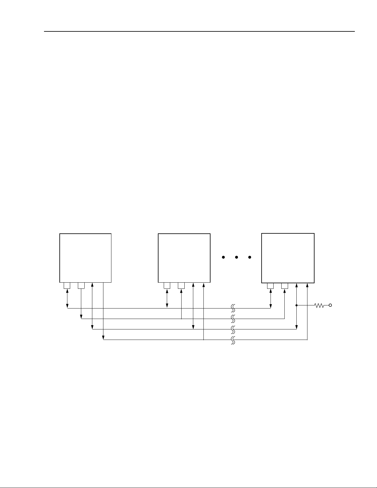
Data Sheet
March 2000 DSP1627 Digital Signal Processor
4 Hardware Architecture
(continued)
In order to prevent multiple bus drivers, only one DSP
can be programmed to transmit in a particular time slot.
In addition, it is important to note that the address/protocol channel is 3-stated in any time slot that is not being
driven.
Therefore, to prevent spurious inputs, the address/protocol channel should be pulled up to V
with a 5 kΩ re-
DD
sistor, or it should be guaranteed that the bus is driven
in every time slot. (If the SYNC1 signal is externally generated, then this pull-up is required for correct initialization.)
Each SIO also has a fully decoded transmitting address
specified by the srta register transmit address field (bits
7—0). This is used to transmit information regarding the
destination(s) of the data. The fully decoded receive address specified by the srta register receive address field
(bits 15—8) determines which data will be received.
The SIO protocol channel data is controlled via the saddx register. When the saddx register is written, the
lower 8 bits contain the 8-bit protocol field. On a read,
the high-order 8 bits read from saddx are the most recently received protocol field sent from the transmitting
DSP's saddx output register. The low-order 8 bits are
read as 0s.
An example use of the protocol channel is to use the top
3 bits of the saddx value as an encoded source address
for the DSPs on the multiprocessor bus. This leaves the
remaining 5 bits available to convey additional control
information, such as whether the associated field is an
opcode or data, or whether it is the last word in a transfer, etc. Th ese bits c an also be us ed to transf er parit y information about the data. Alternatively, the entire field
can be used for data transmission, boosting the bandwidth of the port by 50%.
Using SIO2
The SIO2 functions the same as the SIO. Please refer
to Pin Multiplexing in Section 4.1 for a description of pin
multiplexing of BIO, PHIF, VEC[3:0], and SIO2.
DO
DI
DSP 0
ICK
OCK
SADD
SYNC
DATA CHANNEL
CLOCK
ADDRESS/PROTOCOL CHANNEL
SYNC SIGNAL
Figure 5. Multiprocessor Communication and Connections
DO
DI
DSP 1
ICK
OCK
SADD
SYNC
DO
DI
DSP 7
ICK
OCK
SADD
SYNC
Ω
5 k
5-4181 (F).a
DD
V
Lucent Technologies Inc. 21
Data Sheet
DSP1627 Digital Signal Processor March 2000
4 Hardware Architecture
(continued)
4.8 Parallel Host Interface (PHIF)
The DSP1627 has an 8-bit parallel host interface for rapid transfer of data with external devices. This parallel port
is passive (data strobes provided by an external device)
and supports either
tocols. The PHIF also provides for 8-bit or 16-bit data
transfers. As a flexible hos t int erf ac e, it requires little or
no glue logic to interface to other devices (e.g., microcontrollers, microprocesso rs , o r another DSP).
The data path of the PHIF consists of a 16-bit input buff-
pdx0
er,
output pins, parallel input buffer full (PIBF) and parallel
output buffer empty (POBE), indicate the state of the
buffers. In addition, there are two registers used to control and monitor the PHIF's operation: the parallel host interface control register (
PHIF status register (PSTAT, see Table 8). The PSTAT
register, which reflects the state of the PIBF and POBE
flags, can only be read by an external device when the
PSTAT input pin is asserted. The
the programmable optio ns fo r th is port .
The function of the pins, PIDS and PODS, is programmable to support both the
pin, PCSN, is an input that, when low, enables PIDS and
PODS (or PRWN and PDS, depending on the protocol
used). While PCSN is high, the DSP1627 ignores any activity on PIDS and/or PODS. If a DSP1627 is intended to
be continuously accessed through the PHIF port, PCSN
should be grounded. If PCSN is low and their respective
bits in the
PODS by an external device causes the DSP1627 device to recognize an interru pt .
Programmability
(in), and a 16-bit output bu ffer,
inc
Motorola
register are set, the assertion of PIDS and
or
Intel
microcontroller pro-
phifc
, see Table 28), and the
phifc
Intel
and
Motorola
pdx0
(out). Tw o
register defines
protocols. The
register. Setting PMODE selects 16-bit transfer mode.
An input pin controlled by the host, PBSEL, determines
an access of either the high or low bytes. The assertion
level of the PBSEL input pin is configurable in software
using bit 3 of the
marizes the port's functionality as controlled by the
PSTAT and PBSEL pins and the PBSELF and PMO DE
fields.
For 16-bit transfers, if PBS ELF is zero, the PIBF and
POBE flags are set after the high byte is transferred. If
PBSELF is one, the flags a re s et after the low byte is
transferred. In 8-bit mode, only the low byte is accessed,
and every completion of an input or output access sets
PIBF or POBE.
Bit 1 of the
to operate either with an
chip select (PCSN) and either of the data strobes (PIDS
or PODS) are needed to make an access, or with a
torola
protocol where the chip se lec t (PC SN ), a data
strobe (PDS), and a read/write strobe (PRWN) are needed. PIDS and PODS are negative assertion data strobes
while the assertion level o f PDS is programmable
through bit 2, PSTRB, of the
Finally, the assertion leve l of th e out put pins, PIBF and
POBE, is controlled through bit 4, PFLAG. When PFLAG
is set low, PIBF and POBE output pins have positive assertion levels. By setting bit 5, PF LAGSEL, the logical
OR of PIBF and POBE flags (positive assertion) is seen
at the output pin PIBF. By setting bit 7 in
the polarity of the POBE fla g in t he s t at us register,
PSTAT, can be changed. PSOBEF has no effect on the
POBE pin.
Pin Multiplexing
Please refer to Pin Multiplex ing in Section 4.1 for a description of BIO, PHIF, VE C [3 :0 ], and SIO2 pins.
phifc
register, PBSELF. Table 7 sum-
phifc
register, PSTROBE, configures the port
Intel
protocol where only the
phifc
register.
phifc
Mo-
, PSOBEF,
The parallel host interfac e c an be programmed for 8-bit
or 16-bit data transfers using bit 0, PMODE, of the
phifc
Table 7. PHIF Function (8-bit and 16-bit Modes)
PMODE Field PSTAT Pin PBSEL Pin PBSELF Field = 0 PBSELF Field = 1
0 (8-bit) 0 0 pdx0 low byte reserved
0 0 1 reserved pdx0 low byte
010PSTATreserved
0 1 1 reserved PSTAT
1 (16-bit) 0 0 pdx0 low byte pdx0 high byte
1 0 1 pdx0 high byte pdx0 low byte
110PSTATreserved
1 1 1 reserved PSTAT
Table 8. pstat Register as Seen on PB[7:0]
Bit
Field
76543 2 1 0
RESERVED PIBF POBE
22 Lucent Technologies Inc.

Data Sheet
March 2000 DSP1627 Digital Signal Processor
4 Hardware Architecture
(continued)
4.9 Bit Input/Output Unit (BIO)
The BIO controls the directions of eight bidirectional control I/O pins, IOBIT[7:0]. If a pin is configured as an output,
it can be individually set, c leared, or toggled. If a pin is
configured as an input , it ca n be read and/or tested.
The lower half of the
current values (VALUE[7:0]) of the eight bidirectional pins
IOBIT[7:0]. The uppe r half of th e
REC[7:0]) controls the direction of each of the pins. A logic 1 configures the corresponding pin as an output; a logic
0 configures it as an input. The upper half of the
ister is cleared upon reset .
cbit
The
MODE/MASK[7:0] and DATA/PAT[7:0]. The values of
DATA/PAT[7:0] are cleared upon reset. The meaning of a
bit in either field depends on w hether it has been configured as an input or an output in
figured to be an output, th e m eanings are MODE and
DATA. For an input, the m eanings are MASK and PAT
(pattern). Table 9 show s the functionality of the MOD E/
MASK and DATA/PAT bit s bas ed on the direction selected for the associated IOBIT pin.
Those bits that have been configured as inputs can be individually tested for 1 or 0. For those inputs that are being
tested, there are four flags produced: allt (all true), allf (all
false), somet (some true), and somef (some false). These
flags can be used for cond it ional branch or special instructions. The state of these flags can be saved and restored by reading and writing bits 0 to 3 of the
(see Table 35).
register (see Table 34) contains two 8-bit fields,
sbit
register (see Table 33) contains
sbit
register (DI-
sbit
. If a pin has been con-
alf
sbit
reg-
register
4.10 Timer
The interrupt timer is composed of the timerc (control)
register, the timer0 register, the prescaler, and the
counter itself. The timer control register (see Table 31,
timerc Register) sets up the operational state of the timer
and prescaler. The timer0 register is used to hold the
counter reload value (or period register) and to set the
initial value of the counter. The prescaler slows the clock
to the timer by a number of binary divisors to allow for a
wide range of interrupt delay periods.
The counter is a 16-bit down counter that can be loaded
with an arbitrary number from software. It counts down
to 0 at the clock rate provided by the prescaler. Upon
reaching 0 count, a vectored interrupt to program address 0x10 is issued to the DSP1627, providing the interrupt is enabled (bit 8 of inc and ins registers). The
counter will then either wait in an inactive state for another command from software, or will automatically repeat
the last interrupting period, depending upon the state of
the RELOAD bit in the timerc register.
When RELOAD is 0, the counter counts down from its
initial value to 0, interrupts the DSP1627, and then stops,
remaining inactive until another value is written to the
timer0 register. Writing to the timer0 register causes
both the counter and the period register to be written with
the specified 16-bit number. When RELOAD is 1, the
counter counts down from its initial value to 0, interrupts
the DSP1627, automatically reloads the specified initial
value from the period register into the counter, and repeats indefinitely. This provides for either a single timed
interrupt event or a regular interrupt clock of arbitrary period.
Table 9. BIO Operations
DIREC[n]
MODE/
MASK[n]
DATA/
PAT[n]
Action
*
1 (Output) 0 0 Clear
1 (Output) 0 1 Set
1 (Output) 1 0 No Change
1 (Output) 1 1 Toggle
0 (Input) 0 0 No Test
0 (Input) 0 1 No Test
0 (Input) 1 0 Test for Zero
0 (Input) 1 1 Test for One
*0 ≤ n ≤ 7.
If a BIO pin is switched from being configured as an output to being configured as an input and then back to being configured as an output, the pin retains the previous
The timer can be stopped and started by software, and
can be reloaded with a new period at any time. Its count
value, at the time of the read, can also be read by software. Due to pipeline stages, stopping and starting the
timer may result in one inaccurate count or prescaled period. When the DSP1627 is reset, the bottom 6 bits of the
timerc register and the timer0 register and counter are
initialized to 0. This sets the prescaler to CKO/2*, turns
off the reload feature, disables timer counting, and initializes the timer to its inactive state. The act of resetting the
chip does not cause a timer interrupt. Note that the period register is not initialized on reset.
The T0EN bit of the timerc register enables the clock to
the timer. When T0EN is a 1, the timer counts down towards 0. When T0EN is a 0, the timer holds its current
count.
output val ue.
Pin Multiplexing
Please refer to Pin Multiplexing in Section 4.1 for a
description of BIO, PHIF, VEC[3:0], and SIO2 pins.
* Frequency of CKO/2 is equivalent to either CKI/2 for the PLL by-
passed or related to CKI by the PLL multiplying factors. See Section
4.12, Clock Synthesis.
Lucent Technologies Inc. 23

Data Sheet
DSP1627 Digital Signal Processor March 2000
4 Hardware Architecture
(continued)
The PRESCALE field of the timerc register selects one
of 16 possible clock rates for the timer input clock (see
Table 31, timerc Register).
Setting the DISABLE bit of the timerc register to a logic
1 shuts down the timer and the prescaler for power savings. Setting the TIMERDIS, bit 4, in the powerc register
has the same effect of shutting down the timer. The
DISABLE bit and the TIMERDIS bit are cleared by writing a 0 to their respective registers to restore the normal
operating mode.
4.11 JTAG Test Port
The DSP1627 uses a JTAG/
wire test port for self-test and hardware emulation.
There is no separate TRST input pin. An instruction register, a boundary-scan register, a bypass register, and
a device identification register have been implemented.
The device identification register coding for the
DSP1627 is shown in Table 37. The instruction register
(IR) is 4 bits long. The instruction for accessing the device ID is 0xE (1110). The behavior of the instruction
register is summarized in Table 10. Cell 0 is the LSB
(closest to TDO).
IEEE
1149.1 standard four-
The first line shows the cells in the IR that capture from
a parallel input in the capture-IR controller state. The
second line shows the cells that always load a logic 1 in
the capture-IR controller state. The third line shows the
cells that always load a logic 0 in the capture-IR controller state. Cell 3 (MSB of IR) is tied to status signal PINT,
and cell 2 is tied to status signal JINT. The state of these
signals can therefore be captured during capture-IR and
shifted out during SHIFT-IR controller states.
Boundary-Scan Register
All of the chip's inputs and outputs are incorporated in a
JTAG scan path shown in Table 11. The types of
boundary-scan cells are as follows:
■
I = input cell
■
O = 3-state output cell
■
B = bidirectional (I/O) cell
■
OE = 3-state control cell
■
DC = bidirectional control cell
Table 10. JTAG Instruction Register
IR Cell #: 3 2 1 0
Parallel Input? Y Y N N
Always Logic 1? N N N Y
Always Logic 0? N N Y N
24 Lucent Technologies Inc.

Data Sheet
March 2000 DSP1627 Digital Signal Processor
4 Hardware Architecture
(continued)
Note that the direction of shifting is from TDI to cell 104 to cell 103 . . . to cell 0 of TDO.
Table 11. JTAG Boundary-Scan Register
Cell Type Signal Name/Function Cell Type Signal Name/Function
0 OE Controls cells 1, 27—31 69 B OCK2/PCSN*
1 O CKO 70 DC Controls cell 71
2IRSTB 71BDO2/PSTAT*
3 DC Controls cell 4 72 DC Controls cell 73
4 B TRAP 73 B SYNC2/PBSEL*
5I
STOP
†
74 DC Controls cell 75
6 O IACK 75 B ILD2/PIDS*
7 I INT0 76 DC Controls cell 77
8 OE Controls cells 6, 10—25, 49, 50, 78, 79 77 B OLD2/PODS*
9 I INT1 78 O IBF2/ PIBF*
10—25 O AB[0:15] 79 O OBE2/POBE*
26 I EXM 80 DC Controls cell 81
27 O RWN 81 B ICK2/PB0*
28—31 O EROM, ERAMLO, ERAMHI, IO 82 DC Controls cell 83
32—36 B DB[0:4] 83 B DI2/PB1*
37 DC Controls cells 32—36, 38—48 84 DC Controls cell 85
38—48 B DB[5:15] 85 B DOEN2/PB2*
49 O OBE1 86 DC Controls cell 87
50 O IBF1 87 B SADD2/PB3*
51 I DI1 88 DC Controls cell 89
52 DC Controls cell 53 89 B IOBIT0/PB4*
53 B ILD1 90 DC Controls cell 91
54 DC Controls cell 55 91 B IOBIT1/PB5*
55 B ICK1 92 DC Controls cell 93
56 DC Controls cell 57 93 B IOBIT2/PB6*
57 B OCK1 94 DC Controls cell 95
58 DC Controls cell 59 95 B IOBIT3/PB7*
59 B OLD1 96 DC Controls cell 97
60 OE Controls cell 61 97 B VEC3/IOBIT4*
61 O DO1 98 DC Controls cell 99
62 DC Controls cell 63 99 B VEC2/IOBIT5*
63 B SYNC1 100 DC Controls cell 101
64 DC Controls cell 65 101 B VEC1/IOBIT6*
65 B SADD1 102 DC Controls cell 103
66 DC Controls cell 67 103 B VEC0/IOBIT7*
67 B DOEN1 104 I
CKI
‡
68 DC Controls cell 69
* Please refer to Pin Multiplexing in Section 4.1 for a description of pin multiplexing of BIO, PHIF, VEC[3:0], and SIO2.
† Note that shifting a zero into this cell in the mode to scan a zero into the chip will disable the processor clocks just as the STOP pin will.
‡ When the JTAG SAMPLE instruction is used, this cell will have a logic one regardless of the state of the pin.
Lucent Technologies Inc. 25
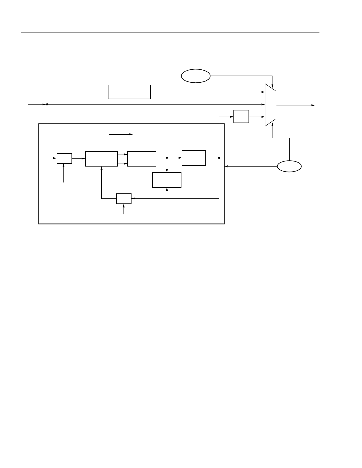
Data Sheet
DSP1627 Digital Signal Processor March 2000
4 Hardware Architecture
4.12 Clock Synthesis
CKI INPUT CLOCK
CKI
f
÷ N
Nbits[2:0]
PHASE
DETECTOR
(continued)
RING
OSCILLATOR
LOCK
(FLAG TO INDICATE LOCK
CONDITION OF PLL)
CHARGE
PUMP
÷ M
LOOP
FILTER
powerc
VCO
VCO CLOCK
VCO
f
SLOWCKI
SLOW CLOCK
f
÷ 2
PLLEN
INTERNAL
PROCESSOR
M
CKI
f
U
X
CLOCK
INTERNAL CLOCK
f
PLLSEL
pllc
PLL/SYNTHESIZER
LF[3:0]Mbits[4:0]
Figure 6. Clock Source Block Diagram
The DSP1627 provides an on-chip, programmable
clock synthesizer. Figure 6 is the clock source diagram.
The 1X CKI input clock, the output of the synthesizer, or
a slow internal ring oscillator can be used as the source
for the internal DSP clock. The clock synthesizer is
based on a phase-locked loop (PLL), and the terms
clock synthesizer and PLL are used interchangeably.
On powerup, CKI is used as the clock source for the
DSP. This clock is used to generate the internal processor clocks and CKO, where f
CKI
= f
. Setting the ap-
CKO
propriate bits in the pllc control register (described in
Table 32) will enable the clock synthesizer to become
the clock source. The powerc register, which is discussed in Section 4.13, can override the selection to
stop clocks or force the use of the slow clock for lowpower operation.
5-4520 (F)
PLL Control Signals
The input to the PLL comes from one of the three maskprogrammable clock options: CMOS, crystal, or smallsignal. The PLL cannot operate without an external input clock.
To use the PLL, the PLL must first be allowed to stabilize and lock to the programmed frequency. After the
PLL has locked, the LOCK flag is set and the lock detect
circuitry is disabled. The synthesizer can then be used
as the clock source. Setting the PLLSEL bit in the pllc
register will switch sources from f
CKI
to f
/2 without
VCO
glitching. It is important to note that the setting of the pllc
register must be maintained. Otherwise, the PLL will
seek the new set point. Every time the pllc register is
written, the LOCK flag is reset.
26 Lucent Technologies Inc.

Data Sheet
March 2000 DSP1627 Digital Signal Processor
4 Hardware Architecture
The frequency of the PLL output clock, f
(continued)
, is deter-
VCO
mined by the values loaded into the 3-bit N divider and
the 5-bit M divider. When the PLL is selected and
locked, the frequency of the internal processor clock is
related to the frequency of CKI by the following equations:
f
= f
.
CKI
* M/N
= f
CKO
VCO
= f
÷ 2
, must fall within the
VCO
VCO
must be at
VCO
INTERNAL CLOCK
f
The frequency of the VCO, f
range listed in Table 63. Also note that f
least twice f
CKI
The coding of the Mbits and Nbits is described as follows:
Mbits = M − 2
if (N == 1)
Nbits = 0x7
else
Nbits = N − 2
where N ranges from 1 to 8 and M ranges from 2 to 20.
The loop filter bits LF[3:0] should be programmed ac-
cording to Table 64.
Two other bits in the pllc register control the PLL. Clearing the PLLEN bit powers down the PLL; setting this bit
powers up the PLL. Clearing the PLLSEL bit deselects
the PLL so that the DSP is clocked by a 1X version of
the CKI input; setting the PLLSEL bit selects the PLLgenerated clock for the source of the DSP internal processor clock. The pllc register is cleared on reset and
powerup. Therefore, the DSP comes out of reset with
the PLL deselected and powered down. M and N should
be changed only while the PLL is deselected. The values of M and N should not be changed when powering
down or deselecting the PLL.
As previously mentioned, the PLL also provides a user
flag, LOCK, to indicate when the loop has locked. When
this flag is not asserted, the PLL output is unstable. The
DSP should not be switched to the PLL-based clock
without first checking that the lock flag is set. The lock
flag is cleared by writing to the pllc register. When the
PLL is deselected, it is necessary to wait for the PLL to
relock before the DSP can be switched to the PLLbased clock. Before the input clock is stopped, the PLL
should be powered down. Otherwise, the LOCK flag will
not be reset and there may be no way to determine if the
PLL is stable, once the input clock is applied again.
The lock-in time depends on the frequency of operation
and the values programmed for M and N (see Table 64).
Lucent Technologies Inc. 27

Data Sheet
DSP1627 Digital Signal Processor March 2000
4 Hardware Architecture
(continued)
PLL Programming Examples
The following section of code illustrates how the PLL would be initialized on powerup, assuming the following operating conditions:
■
CKI input frequency = 10 MHz
■
Internal clock and CKO frequency = 50 MHz
■
VCO frequency = 100 MHz
■
Input divide down count N = 2 (Set
■
Feedback down count M = 20 (Set
Nbits[2:0]
Mbits[4:0]
= 000 to get N = 2, as described in Table 32.)
= 10010 to get M = 18 + 2 = 20, as described in Table 32.)
The device would come out of reset with the PLL disabled and deselected.
pllinit: pllc = 0x2912 /* Running CKI input clock at 10 MHz, set up counters in PLL */
pllc = 0xA912 /* Power on PLL, but PLL remains deselected */
call pllwait /* Loop to check for LOCK flag assertion */
pllc = 0xE912 /* Select high-speed, PLL clock */
goto start /* User's code, now running at 50 MHz */
pllwait: if lock return
goto pllwait
Programming examples which illustrate how to use the PLL with the various power management modes are listed
in Section 4.13.
Latency
The switch between the CKI-based clock and the PLL-based clock is synchronous. This method results in the actual
switch taking place several cycles after the PLLSEL bit is changed. During this time, actual code can be executed,
but it will be at the previous clock rate. Table 12 shows the latency times for switching between CKI-based and PLLbased clocks. In the example given, the delay to switch to the PLL source is 1—4 CKO cycles and to switch back is
11—31 CKO cycles.
Table 12. Latency Times for Switching Between CKI and PLL-Based Clocks
Minimum Latency (Cycles) Maximum Latency (Cycles)
Switch to PLL-based clock 1 N + 2
Switch from PLL-based clock M/N + 1 M + M/N + 1
Frequency Accuracy and Jitter
When using the PLL to multiply the input clock frequency up to the instruction clock rate, it is important to realize
that although the average frequency of the internal clock and CKO will have about the same relative accuracy as
the input clock, noise sources within the DSP will produce jitter on the PLL clock such that each individual clock
period will have some error associated with it. The PLL is guaranteed only to have sufficiently low jitter to operate
the DSP, and thus, this clock should not be used as an input to jitter-sensitive devices in the system.
V
and V
DDA
The PLL has its own power and ground pins, V
form of a ferrite bead connected from V
a 0.01 µF ceramic) from V
Connections
SSA
to VSS. V
DDA
and V
DDA
to VDD and two decoupling capacitors (4.7 µF tantalum in parallel with
DDA
can be connected directly to the main ground plane. This recommen-
SSA
. Additional filtering should be provided for V
SSA
DDA
in the
dation is subject to change and may need to be modified for specific applications depending on the characteristics
of the supply noise.
Note:
For devices with the CMOS clock input option, the CKI2 pin should be connected to V
SSA
.
28 Lucent Technologies Inc.

Data Sheet
March 2000 DSP1627 Digital Signal Processor
4 Hardware Architecture
(continued)
4.13 Power Management
There are three different control mechanisms for putting
the DSP1627 into low-power modes: the powerc control
register, the STOP pin, and the AWAIT bit in the alf register. The PLL can also be disabled with the PLLEN bit
of the pllc register for more power saving.
Powerc Control Register Bits
The powerc register has 10 bits that power down various portions of the chip and select the clock source:
XTLOFF:
crystal oscillator or the small-signal input circuit, disabling the internal processor clock. Assertion of the
XTLOFF bit to disable the crystal oscillator also prevents its use as a noninverting buffer. Since the oscillator and the small-signal input circuits take many cycles
to stabilize, care must be taken with the turn-on sequence, as described later.
SLOWCKI:
ring oscillator as the clock source for the internal processor clock instead of CKI or the PLL. When CKI or the
PLL is selected, the ring oscillator is powered down.
Switching of the clocks is synchronized so that no partial or short clock pulses occur. Two
the instruction that sets or clears SLOWCKI.
NOCK:
off the internal processor clock, regardless of whether
its source is provided by CKI, the PLL, or the ring oscillator. The NOCK bit can be cleared by resetting the chip
with the RSTB pin, or asserting the INT0 or INT1 pins.
Two
The PLL remains running, if enabled, while NOCK is
set.
INT0EN:
clear the NOCK bit, thereby allowing the device to continue program execution from where it left off without
any loss of state. No chip reset is required. It is recommended that, when INT0EN is to be used, the INT0
interrupt be disabled in the inc register so that an unintended interrupt does not occur. After the program resumes, the INT0 interrupt in the ins register should be
cleared.
INT1EN:
NOCK clear, exactly like INT0EN previously described.
The following control bits power down the peripheral
I/O units of the DSP. These bits can be used to further
reduce the power consumption during standard sleep
mode.
Assertion of the XTLOFF bit powers down the
Assertion of the SLOWCKI bit selects the
nop
s should follow
Assertion of the NOCK bit synchronously turns
nop
s should follow the instruction that sets NOCK.
This bit allows the INT0 pin to asynchronously
This bit enables the INT1 pin to be used as the
SIO1DIS:
unit. It disables the clock input to the unit, thus eliminating any sleep power associated with the SIO1. Since
the gating of the clocks may result in incomplete transactions, it is recommended that this option be used in
applications where the SIO1 is not used or when reset
may be used to reenable the SIO1 unit. Otherwise, the
first transaction after reenabling the unit may be corrupted.
SIO2DIS:
way SIO1DIS powers down the SIO1.
PHIFDIS:
host interface. It disables the clock input to the unit, thus
eliminating any sleep power associated with the PHIF.
Since the gating of the clocks may result in incomplete
transactions, it is recommended that this option be used
in applications where the PHIF is not used, or when reset may be used to reenable the PHIF. Otherwise, the
first transaction after reenabling the unit may be corrupted.
TIMERDIS:
the clock input to the timer unit. Its function is identical
to the DISABLE field of the timerc control register. Writing a 0 to the TIMERDIS field will continue the timer operation.
Figure 7 shows a functional view of the effect of the bits
of the powerc register on the clock circuitry. It shows
only the high-level operation of each bit. Not shown are
the bits that power down the peripheral units.
STOP Pin
Assertion (active-low) of the STOP pin has the same effect as setting the NOCK bit in the powerc register. The
internal processor clock is synchronously disabled until
the STOP pin is returned high. Once the STOP pin is returned high, program execution will continue from
where it left off without any loss of state. No chip reset
is required. The PLL remains running, if enabled, during
STOP assertion.
The pllc Register Bits
The PLLEN bit of the pllc register can be used to power
down the clock synthesizer circuitry. Before shutting
down the clock synthesizer circuitry, the system clock
should be switched to either CKI using the PLLSEL bit
of pllc, or to the ring oscillator using the SLOWCKI bit of
powerc.
This is a powerdown signal to the SIO1 I/O
This bit powers down the SIO2 in the same
This is a powerdown signal to the parallel
This is a timer disable signal which disables
Lucent Technologies Inc. 29
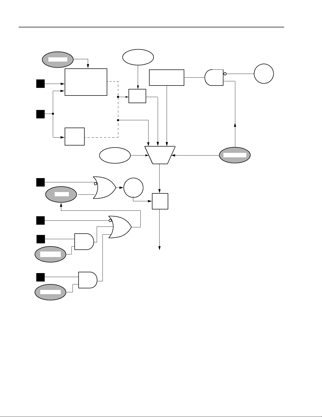
Data Sheet
DSP1627 Digital Signal Processor March 2000
4 Hardware Architecture
CKI2
CKI
STOP
RSTB
XTLOFF
OSCILLATOR,
SMALL SIGNAL
MASK-PROGRAMMABLE
CMOS
INPUT
CLOCK
HW STOP
NOCK
CLEAR NOCK
OFF
CRYSTAL
OR
CLOCK
OPTION
SW STOP
(continued)
PLLSEL
PLLEN
PLL
CKI
f
DEEP
SLEEP
DISABLE
RING
OSCILLATOR
VCO/2
f
SYNC.
MUX
SYNC.
GATE
INTERNAL CLOCK
f
SLOW CLOCK
f
ON
DEEP
SLEEP
SLOWCKI
INT0
INT0EN
INT1
INT1EN
Notes:
The functions in the shaded ovals are bits in the powerc control register. The functions in the nonshaded ovals are bits in the pllc control
register.
Deep sleep is the state arrived at either by a hardware or software stop of the internal processor clock.
The switching of the multiplexers and the synchronous gate is designed so that no partial clocks or glitching will occur.
When the deep sleep state is entered with the ring oscillator selected, the internal processor clock is turned off before the ring oscillator is pow-
ered down.
PLL select is the PLLSEL bit of pllc; PLL powerdown is the PLLEN bit of pllc.
INTERNAL
PROCESSOR
CLOCK
5-4124 (F).h
Figure 7. Power Management Using the powerc and the pllc Registers
30 Lucent Technologies Inc.
 Loading...