

AGERE DSP16210 Datasheet

Data Sheet
July 2000
DSP16210 Digital Signal Processor
Features
■ Optimized for applications requiring large internal mem-
ory, flexible I/O, and high cycle efficiency speech coding,
speech compression, and channel coding
— Large on-chip dual-port RAM (60 Kwords of
DPRAM)—eliminates need for fast external SRAM
— 2-input 40-bit arithmetic logic unit (ALU) with
add/compare/select (ACS) for Viterbi acceleration
— 3-input adder
— DMA-based I/O—minimizes DSP core overhead for
I/O processing
— Flexible power management modes for low system
power dissipation
— Provides 200 DSP MIPS
■ 10 ns instruction cycle time at 3 V
■ Dual 16 x 16-bit multiplication and 40-bit accumulation in
one instruction cycle for efficient algorithm implementations
■ 31-instruction by 32-bit interruptible do-loop cache for
high-speed, program-efficient, zero-overhead looping
■ Nested interrupts and three interrupt priority levels for
efficient control and task management operations
■ On-chip boot ROM with hardware development system
and boot code for flexible downloading
■ On-chip, programmable, PLL clock synthesizer
■ Enhanced serial I/O (ESIO) port designed to multi-
plex/demultiplex 64 Kbits/s, 32 Kbits/s, 16 Kbits/s, and 8
Kbits/s channels
■ 26 Mbits/s simple serial I/O (SSIO) port coupled with
DMA to support low-overhead I/O
■ 16-bit parallel host interface (PHIF16) coupled with DMA
to support low-overhead I/O
— Supports either 8-bit or 16-bit external bus configura-
tions (8-bit ex ternal configur at ion supp orts either 8-bit
or 16-bit logical transfers)
— Supports either
■ 8-bit control I/O interface for increased flexibility and
Motorola
lower system costs
■
■ Full-speed in-circuit emulation hardware development
3
IEEE
1149.1 test port (JTAG boundary scan)
system on-chip with eight address and two data watchpoint units for efficient application development
■ Pin compatible with the DSP1620
■ 144-pin TQFP package
1
or
Intel
2
protocols
Description
The DSP16210 is the first DSP device based on the
DSP16000 digital sign al processing core. It is manuf actured
in a 0.35 µm CMOS technology and offers a 10 ns instruction cycle time at 3 V operation. Designed specifically for
applications requiring a large amount of memory, a flexible
DMA-based I/O structure, and high cycle efficiency, the
DSP16210 is a signal coding device that can be programmed to perform a wide variety of fixed-point signal processing functions. The DSP16210 includes a mix of
peripherals specifically intended to support processingintensive but cost-sensitive applications.
The large on-chip RAM (60 Kwords of dual-port RAM) supports downloadable system design—a must for infrastructure applications—to support field upgrades for evolving
coding standards. The DSP16210 can address up to
192 Kwords of external storage in both its code/coefficient
memory address space and data memory address space.
In addition, there is an internal boot ROM (IROM) that
includes system boot code and hardware development system (HDS) code.
This devic e also contain s a bit manipul ation unit (BMU) and
a two-input, 40-bit arithmetic logic unit (ALU) with add/compare/select (ACS) for enhanced signal coding efficiency
and Viterbi acceleration.
To optimize I/O throughput and reduce the I/O service routine burden on the DSP core, the DSP16210 is equipped
with two modular I/O units (MIOUs) that m anag e the sim ple
serial I/O port (SSIO) and the 16-bit parallel host interface
(PHIF16) peripherals . The MIOUs pro vide tr ansparent DMA
transfers between the peripherals and on-chip dual-port
RAM.
The combination of large on -chip RAM, low power dissipation, fast instruction cycle times, and efficient I/O management makes the DSP16210 an ideal solution in a variety of
emerging applications.
1.
Motorola
2.
Intel
IEEE
3.
Electronics Engineers, Inc.
is a registered trademark of Motorola, Inc.
is a registered trademark of Intel Corporation.
is a registered trademark of The Institute of Electrical and
DRAFT COPY

Data Sheet
DSP16210 Digital Signal Processor July 2000
Table of Contents
Contents Page Contents Page
Features...................................................................1
➤➤➤➤
Description ...............................................................1
➤➤➤➤
Notation Conventions...............................................9
➤➤➤➤
Hardware Architecture .............................................9
➤➤➤➤
DSP16210 Architectural Overview .........................9
➤
DSP16000 Core.................................................9
➤
Clock Synthesizer (PLL) ....................................9
➤
Dual-Port RAM (DPRAM) ..................................9
➤
Internal Boot ROM (IROM) ..............................12
➤
IORAM and Modular I/O Units (MIOUs) ..........12
➤
External Memory Interface (EMI).....................12
➤
Bit I/O (BIO) Unit..............................................13
➤
Enhanced Serial I/O (ESIO) Unit .....................13
➤
Simple Serial I/O (SSIO) Unit ..........................13
➤
Parallel Host Interface (PHIF16)......................13
➤
Timers..............................................................13
➤
Test Access Port (JTAG).................................13
➤
Hardware Development System (HDS)...........13
➤
Pin Multiplexing................................................13
➤
DSP16000 Core Architect ural Over v iew .. ...... .......14
➤
System Control and Cache (SYS) ...................14
➤
Data Arithmetic Unit (DAU)..............................14
➤
Y-Memory Space Address Arithmetic
➤
Unit (YAAU) ..................................................15
X-Memory Space Address Arithmetic
➤
Unit (XAAU) ..................................................15
Reset ....................................................................18
➤
Reset After Powerup or Power Interruption.....18
➤
RSTB Pin Reset...............................................18
➤
JTAG Controller Reset.....................................19
➤
Interrupts and Trap...............................................20
➤
Interrupt Registers ...........................................20
➤
Clearing Interrupts ...........................................23
➤
Interrupt Request Clearing Latency.................23
➤
INT[3:0] and TRAP Pins ..................................24
➤
Low-Power Standby Mode...............................24
➤
Memory Maps.......................................................25
➤
Boot from External ROM..................................27
➤
Data Memory Map Selection ...........................27
➤
External Memory Interface (EMI)................... .......27
➤
Latency for Programming
➤
Registers.......................................................27
Programmable Access Time............................28
➤
READY Pin Enables ........................................28
➤
Enable Delays..................................................28
➤
Memory Map Selection ....................................28
➤
RWN Advance .................................................29
➤
CKO Pin Configuration ....................................29
➤
Write Data Drive Delay ....................................29
➤
Functional Timing ............................................29
➤
READY Pin ......................................................31
➤
mwait
and
ioc
Enhanced Serial I/O (ESIO) Unit..........................32
➤
Input Section....................................................32
➤
Output Section.................................................36
➤
Modular I/O Units (MIOUs) ...................................42
➤
IORAM.............................................................42
➤
MIOU Registers ...............................................42
➤
MIOU Commands ............................................43
➤
I/O Buffer Configuration ...................................45
➤
Length Counters and MIOU Interrupts.............46
➤
DMA Input Flow Control...................................46
➤
DMA Output Flow Control................................47
➤
MIOU Performance..........................................47
➤
Powering Down an MIOU ................................47
➤
MIOU Command Latencies..............................48
➤
Simple Serial I/O (SSIO) Unit ...............................49
➤
Programmable Modes......................................49
➤
Parallel Host Interface (PHIF16)...........................49
➤
Programmability...............................................50
➤
Bit Input/Output Unit (BIO)....................................52
➤
Pin Multiplexing................................................53
➤
Timers...................................................................53
➤
Hardware Development System (HDS)................54
➤
JTAG Test Port.....................................................54
➤
Clock Synthesis ....................................................56
➤
Phase-Lock Loop (PLL) Operation ..................58
➤
Phase-Lock Loop (PLL) Operating
➤
Frequency.....................................................58
Phase-Lock Loop (PLL) Locking......................58
➤
Phase-Lock Loop (PLL) Programming
➤
Restrictions ...................................................59
Phase-Lock Loop (PLL) Programming
➤
Example........................................................60
Phase-Lock Loop (PLL) Frequency
➤
Accuracy and Jitter ...................... ....... ...... ....60
Phase-Lock Loop (PLL) Power Connections...60
➤
Power Management..............................................61
➤
powerc
The
➤
STOP Pin.........................................................63
➤
PLL Powerdown...............................................63
➤
AWAIT Bit of the
➤
Power Management Examples........................63
➤
Software Architecture............................ ....... ...... ....69
➤➤➤➤
Instruction Set Quick Reference.......... ....... ...... ....69
➤
Conditions Based on the State of Flags...........85
➤
Registers...............................................................86
➤
Peripheral Register Write-Read Latency .........86
➤
Register Overview............................................86
➤
Register Settings..............................................91
➤
Reset States ................ ...... ....... ...... ....... ...... ..113
➤
RB Field Encoding .........................................115
➤
Pin Information.....................................................116
➤➤➤➤
Control Register Bits ...................61
alf
Register...........................63
2
DRAFT COPY
Lucent Technologies Inc.

Data Sheet
July 2000 DSP16210 Digital Signal Processor
Table of Contents
(continued)
Contents Page Contents Page
Signal Descriptions ..............................................121
➤➤➤➤
System Interface and Control I/O Interface ........122
➤
System Interface....................................... .....122
➤
Control I/O Interface ......................................122
➤
External Memory Interface... ....... ...... ....... ...... .....123
➤
ESIO Interface....................................................123
➤
SSIO Interface....................................................124
➤
PHIF16 Interface.................................................125
➤
JTAG Test Interface............................................125
➤
DSP16210 Boot Routines ....................................126
➤➤➤➤
Commands .........................................................127
➤
Device Characteristics .........................................133
➤➤➤➤
Absolute Maximum Ratings................................133
➤
Handling Precautions..........................................133
➤
Recommended Operating Conditions.................133
➤
Package Thermal Considerations..................134
➤
Electrical Characteristics and Requirements .......135
➤➤➤➤
Power Dissipation...............................................137
➤
Timing Characteristics and Requirements ...........138
➤➤➤➤
Phase-Lock Loop................................................139
➤
Wake-Up Latency ...............................................140
➤
DSP Clock Generation........................................141
➤
Reset Circuit .......................................................142
➤
Reset Synchronization........................................143
➤
JTAG...................................................................144
➤
Interrupt and Trap...............................................145
➤
Bit I/O..................................................................146
➤
External Memory Interface..................................147
➤
PHIF16................................................................153
➤
Simple Serial I/O.................................................161
➤
Enhanced Serial I/O............................................166
➤
Outline Diagrams..................................................170
➤➤➤➤
144-Pin TQFP Outline Diagram..... ...... ....... ...... ..170
➤
Lucent Technologies Inc.
DRAFT COPY
3

Data Sheet
DSP16210 Digital Signal Processor July 2000
List of Figures
Figures Page
Figure 1. DSP16210 Block Diagram..................................................................................................................10
➤
Figure 2. DSP16000 Core Block Diagram.........................................................................................................16
➤
Figure 3. INT[3:0] and TRAP Timing .................................................................................................................24
➤
Figure 4. Interleaved Internal DPRAM...............................................................................................................25
➤
Figure 5. X-Memory Space Memory Map .........................................................................................................25
➤
Figure 6. Y-Memory Space Memory Maps........................................................................................................26
➤
Figure 7. Input Control Signal Conditioning.......................................................................................................33
➤
Figure 8. Frame Sync Timing with ILEV = ISLEV = 0 and ISDLY = 1................................................................33
➤
Figure 9. Input Functional Timing......................................................................................................................33
➤
Figure 10. Input Demultiplexer (
➤
Figure 11. Serial Input Clocking Example ...........................................................................................................35
➤
Figure 12. Output Control Signal Conditioning....................................................................................................37
➤
Figure 13. Output Functional Timing...................................................................................................................37
➤
Figure 14. Output Multiplexer (
➤
Figure 15. Serial Output Clocking Example.........................................................................................................40
➤
Figure 16. Modular I/O Units ...............................................................................................................................42
➤
Figure 17. Input and Output Buffer Configuration in IORAM
➤
Figure 18. Clock Synthesizer (PLL) Block Diagram.............................................................................................56
➤
Figure 19. Internal Clock Selection and Disable Logic........................................................................................57
➤
Figure 20. Allowable States and State Changes of
➤
Figure 21. Power Management and Clock Distribution........................................................................................62
➤
Figure 22. Interpretation of the Instruction Set Summary Table..........................................................................70
➤
Figure 23. DSP16210 Program-Accessible Registers.........................................................................................87
➤
Figure 24. DSP16210 144-Pin TQFP Pin Diagram (Top View) ........................................................................116
➤
Figure 25. DSP16210 Pinout by Interface.........................................................................................................121
➤
OH
Figure 26. Plot of V
➤
Figure 27. Plot of V
➤
Figure 28. I/O Clock Timing Diagram ................................ ...... ....... ..................................................................141
➤
Figure 29. Powerup Reset and Device Reset Timing Diagram ........................................................................142
➤
Figure 30. Reset Synchronization Timing..........................................................................................................143
➤
Figure 31. JTAG I/O Timing Diagram .............................................. ...... ...... ....... ...... ....... ...... ....... ... ... ....... ...... ..144
➤
Figure 32. Interrupt and Trap Timing Diagram ................................................................................................145
➤
Figure 33. Write Outputs Followed by Read Inputs (
➤
Figure 34. Enable Transition Timing..................................................................................................................147
➤
Figure 35. External Memory Data Read Timing Diagram (No Delayed Enable) ..............................................148
➤
Figure 36. External Memory Data Read Timing Diagram (Delayed Enable) ....................................................149
➤
Figure 37. External Memory Data Write Timing Diagram (DENB2 = 0, DENB1 = 0, DENB0 = 0)....................150
➤
Figure 38. External Memory Data Write Timing Diagram (DENB2 = 0, DENB1 = 1, DENB0 = 0)....................151
➤
Figure 39. READY Extended Read Cycle Timing..............................................................................................152
➤
Figure 40. PHIF16
➤
Figure 41. PHIF16
➤
Figure 42. PHIF16
➤
Figure 43. PHIF16
➤
Figure 44. PHIF16
➤
Figure 45. PIBF and POBE Reset Timing Diagram ..........................................................................................160
➤
Figure 46. POBE and PIBF Disable Timing Diagram........................................................................................160
➤
Figure 47. SSIO Passive Mode Input Timing Diagram .....................................................................................161
➤
Figure 48. SSIO Active Mode Input Timing Diagram ........................................................................................162
➤
Figure 49. SSIO Passive Mode Output Timing Diagram ..................................................................................163
➤
Figure 50. SSIO Active Mode Output Timing Diagram......................................................................................164
➤
Figure 51. Serial I/O Active Mode Clock Timing................................................................................................165
➤
vs. IOH Under Typical Operating Conditions ..................................................................136
OL
vs. IOL Under Typical Operating Conditions....................................................................136
Intel
Mode Signaling (Read and Write) Timing Diagram.....................................................153
Intel
Mode Signaling (Pulse Period and Flags) Timing Diagram ......................................155
Motorola
Motorola
Intel
or
IDMX
) and Register File Structure ....................................................................34
OMX
) and Register File Structure.......................................................................38
〈〈〈〈
〉〉〉〉
0, 1
.......................................................................45
pllc
Register Fields.............................................................59
cbit = IMMEDIATE; a1 = sbit
Mode Signaling (Read and Write) Timing Diagram..............................................156
Mode Signaling (Pulse Period and Flags) Timing Diagram .................................158
Motorola
Mode Signaling (Status Register Read) Timing Diagram .......................159
) Timing Characteristics....146
4
DRAFT COPY
Lucent Technologies Inc.

Data Sheet
July 2000 D SP16210 Digital Signal Processor
List of Figures
(continued)
Figure Page
Figure 52. Simple Mode Input Timing Diagram.................................................................................................166
➤
Figure 53. Simple Mode Output Timing Diagram ..............................................................................................167
➤
Figure 54. Frame Mode Input Timing Diagram..................................................................................................168
➤
Figure 55. Frame Mode Output Timing Diagram...............................................................................................169
➤
Lucent Technologies Inc.
LUCENT TECHNOLOGIES—PROPRIETARY
Use pursuant to Company Instructions
5

Data Sheet
DSP16210 Digital Signal Processor July 2000
List of Tables
Tables Page
Table 1. DSP16210 Block Diagram Legend.................................................................................................... 11
➤
Table 2. DSP16000 Core Block Diagram Legend........................................................................................... 17
➤
Table 3. State of Device Output and Bidirectional Pins During and After Reset............................................. 19
➤
Table 4. Interrupt and User Trap Vector Table................................................................................................ 21
➤
Table 5. Interrupt Control 0 and 1 (
➤
Table 6. Interrupt Status (
➤
Table 7. Interrupt Request Clearing Latency................................................................................................... 23
➤
Table 8. Access Time and Wait-States ........................................................................................................... 28
➤
Table 9. Wait-States........................................................................................................................................ 31
➤
Table 10. ESIO Memory Map (Input Section) ................................................................................................... 32
➤
Table 11. Input Channel Sta rt Bit Registers...................................................................................... ................ 35
➤
Table 12. ESIO Memory Map (Output Section)................................................................................................. 36
➤
Table 13. Output Channel Start Bit Registers ................................................................................................... 39
➤
Table 14. ESIO Interrupts.................................................................................................................................. 41
➤
Table 15. Instructions for Programming MIOU Registers.................................................................................. 42
➤
Table 16. MIOU〈0,1〉 16-Bit Directly Program-Accessible Registers................................................................. 43
➤
Table 17. MIOU Write-Only Command-Accessible Registers........................................................................... 43
➤
Table 18. MIOU〈0,1〉 Command (
➤
Table 19. Effect of Reset on MIOU Interrupts and Registers............................................................................ 44
➤
Table 20. MIOU Interrupts................................................................................................................................. 46
➤
Table 21. MIOU Command Latencies............................................................................................................... 48
➤
Table 22. PHIF16 Output Function.................................................................................................................... 51
➤
Table 23. PHIF16 Input Function ...................................................................................................................... 51
➤
Table 24. PHIF16 Status (
➤
Table 25. BIO Operations.................................................................................................................................. 52
➤
Table 26. BIO Flags .......................................................................................................................................... 52
➤
Table 27. JTAG Boundary-Scan Register......................................................................................................... 55
➤
Table 28. Clock Source Selection..................................................................................................................... 56
➤
Table 29.
➤
Table 30. Example Calculation of M and N....................................................................................................... 60
➤
Table 31. DSP16210 Instruction Groups........................................................................................................... 69
➤
Table 32. Instruction Set Summary................................................................................................................... 71
➤
Table 33. Notation Conventions for Instruction Set Descriptions...................................................................... 77
➤
Table 34. Overall Replacement Table............................................................................................................... 78
➤
Table 35. F1 Instruction Syntax......................................................................................................................... 81
➤
Table 36. F1E Function Statement Syntax........................................................................................................ 83
➤
Table 37. DSP16210 Conditional Mnemonics................................................................................................... 85
➤
Table 38. Program-Accessible Registers by Type, Listed Alphabetically ......................................................... 88
➤
Table 39. ESIO Memory-Mapped Registers ..................................................................................................... 90
➤
Table 40. MIOU-Accessible Registers .............................................................................................................. 90
➤
Table 41. DMA-Accessible Registers................................................................................................................ 90
➤
Table 42.
➤
Table 43.
➤
Table 44.
➤
Table 45.
➤
Table 46.
➤
Table 47.
➤
Table 48.
➤
Table 49.
➤
Table 50.
➤
Table 51.ID (JTAG Identification) Register....................................................................................................... 97
➤
pllc
Field Values Nbits[2:0] and Mbits[2:0]........................................................................................ 58
alf
Register........................................................................................................................................ 91
auc0
(Arithmetic Unit Control 0) Register ......................................................................................... 92
auc1
(Arithmetic Unit Control 1) Register ......................................................................................... 93
cbit
(BIO Control) Register ............................................................................................................... 94
cstate
ICR
ICSB
ICSL
ICVV
(Cache State) Register .......................................................................................................... 94
(ESIO Input Control) Register.................................................................................................... 95
0—7
〈〈〈〈
0—1
〈〈〈〈
(ESIO Input Channel Valid Vector) Register............................................................................ 96
ins
PSTAT
〉〉〉〉
(ESIO Input Channel Start Bit) Registers...................................................................... 96
〉〉〉〉
(ESIO Input Channel Sample Length) Registers........................................................... 96
inc0, inc1
) Register........................................................................................................... 22
mcmd
) Register ..................................................................................................... 51
) Registers ............................................................................... 22
0,1
〈〈〈〈
〉〉〉〉
) Register.................................................................................... 44
6
DRAFT COPY
Lucent Technologies Inc.

Data Sheet
July 2000 D SP16210 Digital Signal Processor
List of Tables
(continued)
Tables Page
0—1
Table 52.
➤
Table 53.
➤
Table 54.
➤
Table 55.
➤
Table 56.
➤
Table 57.
➤
Table 58.
➤
Table 59.
➤
Table 60.
➤
Table 61.
➤
Table 62.
➤
Table 63.
➤
Table 64.
➤
Table 65.
➤
Table 66.
➤
Table 67.
➤
Table 68.
➤
Table 69.
➤
Table 70.
➤
Table 71.
➤
Table 72.
➤
Table 73.
➤
Table 74. Core Register States After Reset—40-bit Registers ....................................................................... 113
➤
Table 75. Core Register States After Reset—32-bit Registers ....................................................................... 113
➤
Table 76. Core Register States After Reset—20-bit Registers ....................................................................... 113
➤
Table 77. Core Register States After Reset—16-bit Registers ....................................................................... 114
➤
Table 78. Peripheral (Off-Core) Register States After Reset.......................................................................... 114
➤
Table 79. RB Field.. ......................................................................................................................................... 115
➤
Table 80. Pin Descriptions .............................................................................................................................. 117
➤
Table 81. Command Encoding for Boot Routines........................................................................................... 127
➤
Table 82. Absolute Maximum Ratings............................................................................................................. 133
➤
Table 83. Recommended Operating Conditions ............................................................................................. 133
➤
Table 84. Package Thermal Considerations ................................................................................................... 134
➤
Table 85. Electrical Characteristics and Requirements................................................................................... 135
➤
Table 86. Power Dissipation............................................................................................................................ 137
➤
Table 87. Frequency Ranges for PLL Output.................................................................................................. 139
➤
Table 88. PLL Loop Filter Settings and Lock-In Time..................................................................................... 139
➤
Table 89. Wake-Up Latency............................................................................................................................ 140
➤
Table 90. Timing Requirements for Input Clock.............................................................................................. 141
➤
Table 91. Timing Characteristics for Input Clock and Output Clock................................................................ 141
➤
Table 92. Timing Requirements for Powerup Reset and Device Reset.......................................................... 142
➤
Table 93. Timing Characteristics for Powerup Reset and Device Reset......................................................... 142
➤
Table 94. Timing Requirements for Reset Synchronization Timing ................................................................ 143
➤
Table 95. Timing Requirements for JTAG I/O................................................................................................. 144
➤
Table 96. Timing Characteristics for JTAG I/O................................................................................................ 144
➤
Table 97. Timing Requirements for Interrupt and Trap ................................................................................... 145
➤
Table 98. Timing Characteristics for Interrupt and Trap.................................................................................. 145
➤
Table 99. Timing Requirements for BIO Input Read....................................................................................... 146
➤
Table 100.Timing Characteristics for BIO Output............................................................................................. 146
➤
Table 101.Timing Characteristics for Memory Enables and RWN................................................................... 147
➤
Table 102.Timing Characteristics for External Memory Access (DENB = 0) ....................................................148
➤
inc
ins
ioc
mcmd
miwp
morp
mwait
OCR
OCSB
OCSL
OCVV (
PHIFC
pllc
powerc
PSTAT
psw0
psw1
sbit
SSIOC
timer〈0,1
timer〈0,1〉c
vsw
(
〈〈〈〈
〉〉〉〉
Interrupt Control) Registers ............................................................................................. 97
(Interrupt Status) Register........................................................................................................... 98
(I/O Configuration) Register........................................................................................................ 99
0—1
〈〈〈〈
〉〉〉〉
(MIOU
0—1
〈〈〈〈
〉〉〉〉
(MIOU
0—1
〈〈〈〈
〉〉〉〉
(MIOU
(EMI Configuration) Register................................................................................................ 101
(ESIO Output Control) Register.............................................................................................. 102
0—7
〈〈〈〈
〉〉〉〉
(ESIO Output Channel Start Bit) Registers ............................................................... 103
0—1
〈〈〈〈
〉〉〉〉
(ESIO Output Channel Sample Length) Registers .................................................... 103
ESIO Output Channel Valid Vector) Register ..................................................................... 103
(PHIF16 Control) Register................................................................................................... 104
(Phase-Lock Loop Control) Register........................................................................................ 105
(Power Control) Register ................................................................................................... 106
(PHIF16 Status) Register ................................................................................................... 106
(Processor Status Word 0) Register...................................................................................... 107
(Processor Status Word 1) Register...................................................................................... 108
(BIO Status/Control) Register.................................................................................................. 109
(SSIO Control) Register ...................................................................................................... 110
〉
(TIMER〈0,1〉 Running Count) Register........................................................................... 111
(TIMER〈0,1〉 Control) Register ..................................................................................... 111
(Viterbi Support Word) Register .............................................................................................. 112
〈〈〈〈
〉〉〉〉
0—1
Command) Registers .......................................................................... 100
〈〈〈〈
〉〉〉〉
0—1
IORAM Input Write Pointer) Registers.................................................. 100
〈〈〈〈
〉〉〉〉
0—1
IORAM Output Read Pointer) Registers............................................... 101
Lucent Technologies Inc.
DRAFT COPY
7

Data Sheet
DSP16210 Digital Signal Processor July 2000
List of Tables
(continued)
Tables Page
Table 103.Timing Requirements for External Memory Read (DENB = 0).........................................................148
➤
Table 104.Timing Characteristics for External Memory Access (DENB = 1) ....................................................149
➤
Table 105.Timing Requirements for External Memory Read (DENB = 1).........................................................149
➤
Table 106.Timing Characteristics for External Memory Data Write (RWNADV = 0, DENB = 0)...................... 150
➤
Table 107.Timing Characteristics for External Memory Data Write (RWNADV = 1, DENB = 1)...................... 151
➤
Table 108.Timing Requirements for READY Extended Read Cycle Timing.................................................... 152
➤
Intel
Table 109.Timing Requirements for PHIF16
➤
Table 110.Timing Characteristics for PHIF16
➤
Table 111.Timing Requirements for PHIF16
➤
Table 112.Timing Characteristics for PHIF16
➤
Table 113.Timing Requirements for PHIF16
➤
Table 114.Timing Characteristics for PHIF16
➤
Table 115.Timing Characteristics for PHIF16
➤
Table 116.Timing Requirements for PHIF16
➤
Intel
Intel
and
and
Table 117.Timing Requirements for
➤
Table 118.Timing Characteristics for
➤
Table 119.PHIF16 Timing Characteristics for PIBF and POBE Reset............................................................. 160
➤
Table 120.PHIF16 Timing Characteristics for POBE and PIBF Disable .......................................................... 160
➤
Table 121.Timing Requirements for Serial Inputs (Passive Mode).................................................................. 161
➤
Table 122.Timing Characteristics for Serial Outputs (Passive Mode).............................................................. 161
➤
Table 123.Timing Requirements for Serial Inputs (Active Mode)..................................................................... 162
➤
Table 124.Timing Characteristics for Serial Outputs (Active Mode) ................................................................ 162
➤
Table 125.Timing Requirements for Serial Inputs (Passive Mode).................................................................. 163
➤
Table 126.Timing Characteristics for Serial Outputs (Passive Mode).............................................................. 163
➤
Table 127.Timing Characteristics for Serial Output (Active Mode) .................................................................. 164
➤
Table 128.Timing Characteristics for Signal Generation (Active Mode) .......................................................... 165
➤
Table 129.Timing Requirements for ESIO Simple Input Mode ........................................................................ 166
➤
Table 130.Timing Characteristics for ESIO Simple Input Mode....................................................................... 166
➤
Table 131.Timing Requirements for ESIO Simple Output Mode ..................................................................... 167
➤
Table 132.Timing Characteristics for ESIO Simple Output Mode.................................................................... 167
➤
Table 133.Timing Requirements for ESIO Frame Input Mode......................................................................... 168
➤
Table 134.Timing Characteristics for ESIO Frame Input Mode ....................................................................... 168
➤
Table 135.Timing Requirements for ESIO Frame Output Mode ...................................................................... 169
➤
Table 136.Timing Characteristics for ESIO Frame Output Mode..................................................................... 169
➤
Mode Signaling (Read and Write)...................................... 153
Intel
Mode Signaling (Read and Write) .................................... 154
Intel
Mode Signaling (Pulse Period and Flags).......................... 155
Intel
Mode Signaling (Pulse Period and Flags)........................ 155
Motorola
Motorola
Motorola
Motorola
Motorola
Mode Signaling (Read and Write)............................... 156
Mode Signaling (Pulse Period and Flags) .................. 158
Motorola
Mode Signaling (Read and Write)............................. 157
Mode Signaling (Pulse Period and Flags)................. 158
Mode Signaling (Status Register Read).................... 159
Mode Signaling (Status Register Read) .................. 159
8
DRAFT COPY
Lucent Technologies Inc.

Data Sheet
July 2000 D SP16210 Digital Signal Processor
Notation Conventions
The following notation conventions apply to this data
sheet:
lower-case Registers that are directly writable or
readable by DSP16210 core instructions are lower-case.
UPPER-CASE Device flags, I/O pins, and registers
that are not directly writable or readable by DSP16210 core instructions
are upper-case.
boldface
italics
courier
[ ] Square brackets enclose a range of
〈〉
Register names and DSP16210 core
instructions are printed in boldface
when used in text descriptions.
Documentation varia ble s that are replaced are printed in italics.
DSP16210 program examples are
printed in courier font.
numbers that represents multiple bits in
a single register or bus. The range of
numbers is delimited by a colon. For
example,
program-accessible
Angle brackets enclose a list of items
delimited by commas or a range of
items delimited by a dash (—), one of
which is selected if used in an
instruction. For example,
represents the eight memory-mapped
registers
and the general instruction
aTE
a0h = timer0
ioc
ICSB0, ICSB1
h,l〉=RB
〈
[7:5] are bits 7—5 of the
ioc
register.
ICSB
0—7
〈
ICSB7
, ...,
can be replaced with
.
〉
,
Hardware Architecture
The DSP16210 device is a 16-bit fixed-point programmable digital signal processor (DSP). The DSP16210
consists of a DSP16000 core together with on-chip
memory and peripherals. Advanced architectural features with an expanded instruction set deliver a dramatic increase in performance for signal coding
algorithms. This increase in performance together with
an efficient design implementation results in an
extremely cost- and power-efficient solution for wireless
and multimedia applications.
DSP16210 Architectural Overview
Figure 1 on page 10 shows a block diagram of the
DSP16210. The following blocks make up this device.
DSP16000 Core
The DSP16000 core is the signal-processing engine of
the DSP16210. It is a modified Harvard architecture
with separate sets of buses for the instruction/coefficient (X-memory) and data (Y-memory) spaces. Each
set of buses has 20 bits of address and 32 bits of data.
The core contains data and address arithmetic units
and control for on-chip memory and peripherals.
Clock Synthesizer (PLL)
The DSP16210 exits device reset with an input clock
(CKI) as th e source for the internal clock (CLK). An onchip clock synthesizer (PLL) that runs at a frequency
multiple of CKI can also be used to generate CLK. The
clock synthesizer is deselected and powered down on
reset. For low-power operation, an internally generated
slow clock can drive the DSP.
The clock synthesizer and other programmable clock
sources are discussed in Clock Synthesis beginning on
page 56. The use of these programmable clock
sources for power management is discussed in Power
Management beginning on page 61.
Dual-Port RAM (DPRAM)
This block contains 60 banks (banks 1—60) of zero
wait-state memory. Each bank consists of 1K 16-bit
words and has separate address and data ports to the
instruction/coefficient (X-memory) and data (Y-memory) spaces. DPRAM is organized into even and odd
interleaved banks where each ev en/odd pair is a 32-bit
wide module (see Figure 4 on page 25 for details).
Placing instructions and Y-memory data in the same 2K
module of DPRAM is not supported and may cause
undefined results.
A program can be downloaded from slow off-chip memory into DPRAM, and then executed without waitstates. DPRAM is also useful for improving convolution
performance in cases where the coefficients are adaptive. Since DPRAM can be downloaded through the
JTAG port, full-speed remote in-circuit emulation is
possible.
Lucent Technologies Inc.
DRAFT COPY
9
Data Sheet
DSP16210 Digital Signal Processor July 2000
Hardware Architecture
(continued)
DSP16210 Architectural Overview
IROM
8K x 16
32
ioc
mwait
ESIO
〈
0—15
ICR
ICVV
OCR
20
32
20
EDBEAB
‡
〉
‡
〉
‡
〉
‡
‡
‡
〉
‡
〉
‡
〉
‡
‡
ERAMLO
READY
ERAMHI
EROM
ERAM
EXM
RWN
AB[15:0]
DB[15:0]
EDI
EIFS
EIBC
EIBF
EDO
EOFS
EOBC
EOEB
EOBE
DPRAM
60K x 16
BANKS 1—60
EXTERNAL
MEMORY
INTERFACE
IO
IDMX
ICSB〈0—7
ICSL〈0—1
OMX〈0—15
OCSB〈0—7
OCSL〈0—1
OCVV
(continued)
INT[3:0]
TRAPIACK
INTERRUPT
LOGIC
VEC[3:0]
XDB
XAB
YDB
YAB
10
16
IORAM0
1K x 16
MIOU0
mcmd0
miwp0
morp0
PHIFC
STOP
RSTB
CLOCK SELECTION
AND SYNTHESIS (PLL)
powerc
DSP16000 CORE
TIMER0
timer0c
timer0
‡
PSTAT
CKO
pllc
CLK
TIMER1
timer1c
timer1
§
CKI
IDB
IORAM1
1K x 16
MIOU1
mcmd1
miwp1
morp1
PHIF16
PDX(in)
IOBIT[7:4]/
†
VEC[3:0]
BIO
sbit
cbit
BOUNDARY SCAN
‡
PDX(out)
IOBIT[3:0]
JTAG
jiob
§
ID
HDS
SSIO
SSDX(in)
SSDX(out)
SSIOC
‡
TDO
§
‡
‡
‡
TDI
TCK
TMS
TRST
DI
ICK
ILD
IBF
DO
OCK
OLD
OBE
DOEN
SYNC
PB[15:0] PIDS PODS PCSN PSTATPBSEL
† VEC0 corresponds to IOBIT7, VEC1 corresponds to IOBIT6, VEC2 corresponds to IOBIT5, and VEC3 corresponds to IOBIT4.
‡ These registers are not directly program accessible.
§ These registers are accessible through pins only.
Figure 1. DSP16210 Block Diagram
10
DRAFT COPY
PIBFPOBE
Lucent Technologies Inc.

Data Sheet
July 2000 D SP16210 Digital Signal Processor
Hardware Architecture
DSP16210 Architectural Overview
Table 1. DSP16210 Block Diagram Legend
Symbol Description
BIO Bit I/O Unit
cbit
CLK Internal Clock Signal
DPRAM Dual-por t Rand om- A cces s Mem ory
EAB EMI Address Bus
EDB EMI Data Bus
ESIO Enhanced Serial I/O Unit
HDS Hardware Development System Unit
ICR
ICSB
0—7
〈
ICSL
0—1
〈
ICVV
IDMX
0—15
〈
ID
IDB Internal Data Bus
ioc
IORAM0 Internal I/O RAM 0: Shared with MIOU0
IORAM1 Internal I/O RAM 1: Shared with MIOU1
IROM Internal Boot Read-Only Memory
jiob
JTAG JTAG Test Port
MIOU0 Modular I/O Unit 0: Controls PHIF16
mcmd0
miwp0
morp0
MIOU1 Modular I/O Unit 1: Controls SSIO
mcmd1
miwp1
morp1
mwait
OCR
OCSB
OCSL
OMX
0—7
〈
0—1
〈
OCVV
0—15
〈
PDX
(in) PHIF16 Input Register; Readable by MIOU0
PDX
(out) PHIF16 Output Register; Writable by MIOU0
PHIF16 16-bit Parallel Host Interface
PHIFC
PLL Phase-Lock Loop
pllc
BIO Control Register
ESIO Input Control Register
〉
ESIO Input Channel Start Bit Registers
〉
ESIO Input Channel Sample Length Registers
ESIO Input Channel Valid Vector Register
〉
ESIO Input Demultiplexer Registers
JTAG Device Identification Register
I/O Configuration Register
JTAG Test Register
MIOU0 Command Register
MIOU0 IORAM0 Input Write Pointer
MIOU0 IORAM0 Output Read Pointer
MIOU1 Command Register
MIOU1 IORAM1 Input Write Pointer
MIOU1 IORAM1 Output Read Pointer
EMI Configuration Register
ESIO Output Control Register
〉
ESIO Output Channel Start Bit Registers
〉
ESIO Output Channel Sample Length Registers
ESIO Output Channel Valid Vector Register
〉
ESIO Output Multiplexer Registers
PHIF16 Control Register: Programmed Through MIOU0
Phase-Lock Loop Control Register
(continued)
(continued)
Lucent Technologies Inc.
DRAFT COPY
11

Data Sheet
DSP16210 Digital S ignal Processor July 2000
Hardware Architecture
DSP16210 Architectural Overview
Table 1. DSP16210 Block Diagram Legend
Symbol Description
powerc
PSTAT
sbit
SSDX
(in) SSIO Input Register; Readable by MIOU1
SSDX
(out) SSIO Output Register; Writable by MIOU1
SSIO Simple Serial I/O Unit
SSIOC
TIMER0 Programmable Timer 0
timer0
timer0c
TIMER1 Programmable Timer 1
timer1
timer1c
XAB X-Memory Space Address Bus
XDB X-Memory Space Data Bus
YAB Y-Memory Space Address Bus
YDB Y-Memory Space Data Bus
Power Control Register
PHIF16 Status Register
BIO Status/Control Regi st er
SSIO Control Register: Programmed Through MIOU1
Timer Running Count Register for TIMER0
Timer Control Register for TIMER0
Timer Running Count Register for TIMER1
Timer Control Register for TIMER1
(continued)
(continued)
(continued)
Internal Boot ROM (IROM)
The DSP16210 includes a boot ROM that contains
hardware development code and boot routines. The
boot routines are available for use by the programmer
and are detailed in DSP16210 Boot Routines begin-
ning on page 126.
IORAM and Modular I/O Units (MIOUs)
IORAM storage consists of two 1 Kword banks of memory , IORAM0 and IORAM1. Each IORAM bank has two
16-bit data and two 10-bit address ports; an IORAM
bank can be shared with the core and a modular I/O
unit (MIOU) to implement a DMA-based I/O system.
IORAM supports concurrent core execution and MIOU
I/O processing.
MIOU0 (controls PHIF16) is attached to IORAM0;
MIOU1 (controls SSIO) is attached to IORAM1. Portions of IORAM not dedicated to I/O processing can be
used as general-purpose data storage.
Placing instructions and Y-memory data in the same
IORAM is not supported and may cause undefined
results.
The IORAMs and MIOUs are described in detail in
Modular I/O Units (MIOUs) beginning on page 42.
External Memory Interface (EMI)
The EMI connects the DSP16210 to external memory
and I/O devices. It multiplexes the two sets of core
buses (X and Y) onto a single set of external buses—a
16-bit address bus (AB[15:0]) and 16-bit data bus
(DB[15:0]). These external buses can access external
RAM (ERAMHI/ERAMLO), external ROM (EROM), and
memory-mapped I/O space (IO).
The EMI also manages the on-chip IORAM and ESIO
storage. It multiplexes the two sets of core buses onto a
single set of internal buses—a 10-bit address bus
(EAB[9:0]) and 16-bit data bus (EDB[15:0])—to interface to the IORAMs and ESIO memory-mapped registers.
Instructions can transparently reference external memory, IORAM, and ESIO storage from either set of core
buses. The EMI automatically translates a single 32-bit
access into two 16-bit accesses and vice versa.
The EMI is described in detail in External Memory
Interface (EMI) beginning on page 27.
12
DRAFT COPY
Lucent Technologies Inc.

Data Sheet
July 2000 D SP16210 Digital Signal Processor
Hardware Architecture
DSP16210 Architectural Overview
Bit I/O (BIO) Unit
The BIO unit provides convenient and efficient monitoring and control of eight individually configurable pins
(IOBIT[7:0]). When configured as outputs, the pins can
be individually set, cleared, or toggled. When configured as inputs, individual pins or combinations of pins
can be tested for patterns. Flags returned by the BIO
are testable by conditional instructions. See Bit
Input/Output Unit (BIO) beginning on page 52 for more
details.
Enhanced Serial I/O (ESIO) Unit
The ESIO is a programmable, hardware-managed,
passive, double-buffered full-duplex serial input/output
port designed to support glueless multichannel I/O processing on a TDM (time-division multiplex) highway. In
simple mode, the ESIO supports data rates of up to
26 Mbits/s for a single channel with either 8-bit or 16-bit
data lengths. In frame mode, the ESIO processes up to
16 logical TDM channels with a data rate of up to
8.192 Mbits/s. For more information on the ESIO, see
Enhanced Serial I/O (ESIO) Unit beginning on
page 32.
Simple Serial I/O (SSIO) Unit
The SSIO unit offers a full-duplex, double-buffered
external channel that operates at up to 26 Mbits/s.
Commercially available codecs and time-division multiplex channels can be interfaced to the SSIO with few, if
any, additional components.
The SSIO is a DMA peripheral managed by MIOU1.
See Simple Serial I/O (SSIO) Unit beginning on
page 49 for more information.
Parallel Host Interface (PHIF16)
The PHIF16 is a DMA peripheral managed by MIOU0.
It is a passive 16-bit parallel port that can be configured
to interface to either an 8- or 16-bit external bus containing other Lucent Technologies DSPs, microprocessors, or off-chip I/O devices. The PHIF16 port supports
either
Motorola
or
Intel
protocols.
(continued)
(continued)
or low byte access; in 8-bit mode, only the low byte is
accessed.
Additional software-programmable features allow for a
glueless host interface to microprocessors (see Parallel
Host Interface (PHIF16) beginning on page 49).
Timers
The two timers can be used to provide an interrupt,
either single or repetitive, at the expiration of a programmed interval. More than nine orders of magnitude
of interval selection are provided. The timers can be
stopped and restarted at any time under program control. See Timers beginning on page 53 for more information.
Test Access Port (JTAG)
The DSP16210 provides a test access port that conforms to
boundary scan test access and also controls the Hardware Development System (HDS). See JTAG Test Port
beginning on page 54 for details.
Hardware Development System (HDS)
The HDS is an on-chip hardware module available for
debugging assembly-language programs that execute
on the DSP16000 core in real-time. The main capability
of the HDS is in allowing controlled visibility into the
core’s state during program execution. The HDS is
enhanced with powerful debugging capabilities such as
complex breakpointing conditions, multiple
data/address watchpoint registers, and an intelligent
trace mechanism for recording discontinuities. See
Hardware Development System (HDS) beginning on
page 54 for details.
Pin Multiplexing
The upper four BIO pins (IOBIT[7:4]) are multiplexed
with the vectored interrupt identification pins
(VEC[3:0]). Specifically, VEC0 is multiplexed with
IOBIT7, VEC1 with IOBIT6, VEC2 with IOBIT5, and
VEC3 with IOBIT4. VEC[3:0] are connected to the
package pins and IOBIT[7:4] are disconnected immediately after device reset. To select IOBIT[7:4] to be connected to these pins, the program must set EBIO (bit 8
of the
IEEE
ioc
register).
1149.1 (JTAG). The JTAG port provides
When operating in the 16-bit external bus configuration, PHIF16 can be programmed to swap high and low
bytes. When operating in 8-bit external bus configuration, PHIF16 is accessed in either an 8-bit or 16-bit logical mode. In 16-bit mode, the host selects either a high
Lucent Technologies Inc.
DRAFT COPY
13

Data Sheet
DSP16210 Digital Signal Processor July 2000
Hardware Architecture
(continued)
DSP16000 Core Architectural Overview
See the
mation Manual for a complete description of the
DSP16000 core. Figure2 on page16 shows a block
diagram of the core that consists of four major blocks:
System Control and Cache (SYS), Data Arithmetic Unit
(DAU), Y-Memory Space Address Arithmetic Unit
(YAAU), and X-Memory Space Address Arithmetic Unit
(XAAU). Bits within the
figure the DAU mode-controlled operations.
System Control and Cache (SYS)
This section consists of the control block and the
cache.
The control block provides overall system coordination
that is mostly invisible to the user. The control block
includes an instruction decoder and sequencer, a
pseudorandom sequence generator (PSG), an interrupt and trap handler, a wait-state generator, and lowpower standby mode control logic. An interrupt and trap
handler provides a user-locatable vector table and
three levels of user-assigned interrupt priority.
SYS contains the
that contains AWAIT, a power-saving standby mode
bit, and peripheral flags. The
are 20-bit interrupt control registers, and
interrupt status register.
Programs use the instruction cache to store and execute repetitive operations such as those found in an
FIR or IIR filter section. The cache can contain up to 31
16-bit and 32-bit instructions. The code in the cache
can repeat up to 2
head. Operations in the cache that require a coefficient
access execute at twice the normal rate because the
XAAU and its associated bus are not needed for fetching instructions. The cache greatly reduces the need
for writing in-line repetitive code and, therefore,
reduces instruction/coefficient memory size requirements. In addition, the use of cache reduces power
consumption because it eliminates memory accesses
for instruction fetches.
The
cstate
The 32-bit
instruction following the loop instruction in Xmemory.The cache provides a convenient, low-overhead looping structure that is interruptible, savable, and
restorable. The cache is addressable in both the X and
DSP16000 Digital Signal Processor Core
auc0
alf
register, which is a 16-bit register
16
– 1 times without looping over-
cloop
register controls the cache loop count. The
register contains the current state of the cache.
csave
register holds the opcode of the
and
inc0
auc1
registers con-
inc1
and
ins
registers
is a 20-bit
Info r -
Y memory spaces. An interrupt or trap handling routine
can save and restore
contents of the cache.
Data Arithmetic Unit (DAU)
The DAU is a power-efficient, dual-MAC (multiply/accumulate) parallel-pipelined structure that is tailored to
communications applications. It can perform two double-word (32-bit) fetches, two multiplications, and two
accumulations in a single instruction cycle. The dualMAC parallel pipeline begins with two 32-bit registers, x
and y. The pipeline treats the 32-bit registers as four
16-bit signed registers if used as input to two signed
16-bitx16-bit multipliers. Each multiplier produces a
full 32-bit result stored into registers p0 and p1. The
DAU can direct the output of each multiplier to a 40-bit
ALU or a 40-bit 3-input ADDER.The ALU and ADDER
results are each stored in one of eight 40-bit accumulators, a0 through a7. The ALU includes an ACS
(add/compare/select) function for Viterbi decoding. The
DAU can direct the output of each accumulator to the
ALU/ACS, the ADDER, or a 40-bit BMU (bit manipulation unit).
The ALU implements addition, subtraction, and various
logical operations. To support Viterbi decoding, the
ALU has a split mode in which it computes two simultaneous 16-bit additions or subtractions. This mode,
available in a specialized dual-MAC instruction, is used
to compute the distance between a received symbol
and its estimate.
The ACS provides the add/compare/select function
required for Viterbi decoding. This unit provides flags to
the traceback encoder for implementing mode-controlled side-effects for ACS operations. The source
operands for the ACS are any two accumulators, and
results are written back to one of the source accumulators.
The BMU implements barrel-shift, bit-field insertion, bitfield extraction, exponent extraction, normalization, and
accumulator shuffling operations.
auxiliary registers whose main function is to control
BMU operations.
The user can enable overflow saturation to affect the
multiplier output and the results of the three arithmetic
units. Overflow saturation can also affect an accumulator value as it is transferred to memory or other register.
These features accommodate various speech coding
standards such as GSM-FR, GSM-HR, and GSM-EFR.
Shifting in the arithmetic pipeline occurs at several
stages to accommodate various standards for mixedand double-precision multiplications.
cloop, cstate, csave
ar0
through
, and the
ar3
are
14
DRAFT COPY
Lucent Technologies Inc.

Data Sheet
July 2000 D SP16210 Digital Signal Processor
Hardware Architecture
(continued)
DSP16000 Core Architectural Overview
(continued)
and
and
auc0
auc1
psw1
ar1
auxil-
re1
and
Informa-
,
The DAU contains control and status registers
auc1, psw0, psw1, vsw
The arithmetic unit control registers
select or deselect various modes of DAU operation.
These modes include scaling of the products, saturation on overflow, feedback to the x and y registers fr om
accumulators a6 and a7, simultaneous loading of x and
y
registers with the same value (used for single-cycle
squaring), and clearing the low half of registers when
loading the high half to facilitate fixed-point operations.
The processor status word registers
contain flags set by ALU/ACS, ADDER, or BMU operations. They also include information on the current status of the interrupt controller.
vsw
The
with the traceback encoder. The traceback encoder is a
specialized block for accelerating Viterbi decoding. It
performs mode-controlled side-effects for three MAC
instruction group compare functions:
and
side-effects allow the DAU to store, with no overhead,
state information necessary for traceback decoding.
Side-effects use the c1 counter, the
iary registers, and bits 1 and 0 of
The
used to count events such as the number of times the
program has executed a sequence of code. The c2
register is a holding register for counter c1. Conditional
instructions control these counters and provide a convenient method of program looping.
Y-Memory Space Address Arithmetic Unit (YAAU)
The YAAU supports high-speed, register-indirect, data
memory addressing and postincrementing of the
address register. Eight 20-bit pointer registers (r0—r7)
store read or write addresses for the Y-memory space.
Two sets of 20-bit registers (
define the upper and lower boundaries of two zerooverhead circular buffers for efficient filter implementations. The j and k registers are two 20-bit signed registers that are used to hold user-defined postincrement
values for r0—r7. Fixed increments of +1, –1, 0, +2,
and –2 are also available. (P ostincrement options 0 and
–2 are not available for some specialized transfers. See
the
tion Manual for details.)
register is the Viterbi support word associated
cmp2( )
c1
and
. The
c0
counters are 16-bit signed reg is ter s
DSP16000 Digital Signal Processor Core
, and c0—c2.
auc0
psw0
cmp0( ), cmp1( )
vsw
register controls the modes. The
ar0
and
vsw
.
rb0
and
re0; rb1
The YAAU includes a 20-bit stack pointer (sp). The
data move group includes a set of stack instructions
that consists of push, pop, stack-relative, and pipelined
stack-relative operations. The addressing mode used
for the stack-relative instructions is register-plus-displacement indirect addressing (the displacement is
optional). The displacement is specified as either an
immediate value as part of the instruction or a value
stored in j or k. The YAAU computes the address by
adding the displacement to sp and leaves the contents
of sp unchanged. The data move group also includes
instructions with register-plus-displacement indirect
pt0
r6
and
addressing for the pointer registers r0—
sp
.
The data move group of instructions includes instructions for loading and storing any YAAU register from or
to memory or another core register. It also includes
instructions for loading any YAAU register with an
immediate value stored with the instruction. The
pointer arithmetic group of instructions allows adding of
an immediate value or the contents of the j or k register
to any YAAU pointer register and storing the result to
any YAAU register.
X-Memory Space Address Arithmetic Unit (XAAU)
,
The XAAU contains registers and an adder that control
the sequencing of instructions in the processor. The
program counter (PC) automatically increments
through the instruction space. The interrupt return register pi, the subroutine return register pr, and the trap
return register
return addresses that direct the return to main program
execution from interrupt service routines, subroutines,
and trap service routines, respectively. High-speed,
register-indirect, read-only memory addressing with
postincrementing is done with the
ters. The signed registers h and i are used to hold a
user-defined signed postincrement value. Fixed postincrement values of 0, +1, –1, +2, and –2 are also available. (Postincrement options 0 and –2 are available
only if the target of the data transfer is an accumulator
vector.
Core
)
The data move group of instructions includes instructions for loading and storing any XAAU register from or
to memory or another core register. It also includes
instructions for loading any XAAU register with an
immediate value stored with the instruction.
vbase
programs this register with the base address of the
interrupt and trap vector table.
See the DSP16000 Digital Signal Processor
Information Manual for details.)
is the 20-bit vector base offset register. The user
ptrap
are automatically loaded with
in addition to
pt1
regis-
Lucent Technologies Inc.
DRAFT COPY
15
Data Sheet
DSP16210 Digital Signal Processor July 2000
Hardware Architecture
(continued)
DSP16000 Core Architectural Overview
SYS
XAB
(20)
YAB
DAU
auc0 (16)
auc0 (16)
auc1 (16)
auc1 (16)
psw0 (16)
psw0 (16)
psw1 (16)
psw1 (16)
(20)
XDB
(32)
IDB
(32)
vsw (16)
vsw (16)
c0 (16)
c0 (16)
c1 (16)
c1 (16)
c2 (16)
c2 (16)
ar0 (16)
ar0 (16)
ar1 (16)
ar1 (16)
ar2 (16)
ar2 (16)
ar3 (16)
ar3 (16)
CACHE
31 INSTRUCTIONS
cloop (16)
cloop (16)
cstate (16)
cstate (16)
csave (32)
csave (32)
y (32) x (32)
y (32) x (32)
SHIFT(0, –1) SHIFT(0, –1)
SWAP MUX
16 × 16 MULTIPLY 16 × 16 MULTIPL Y
p0 (32)
p0 (32)
SHIFT(2, 1, 0, –2)/SAT.
SHIFT(2, 1, 0, –2)/SAT.
SHIFT(0, –1)
CONTROL
ins (20)
ins (20)
inc0 (20)
inc0 (20)
inc1 (20)
inc1 (20)
alf (16)
alf (16)
PSG
p1 (32)
p1 (32)
SHIFT(2, 1, 0, –2)/SAT.
SHIFT(2, 1, 0, –2)/SAT.
SHIFT(0, –15, –16)
(continued)
DOUBLE
–2, 0, 2
re0 (20)
re0 (20)
re1 (20)
re1 (20)
h (20)
h (20)
i (20)
i (20)
SINGLE
–1, 0, 1
IMMEDIATE
VALUE
MUX
IMMEDIATE
VALUE
+
PC (20)
pt0 (20)
pt0 (20)
pt1 (20)
pt1 (20)
vbase (20)
vbase (20)
‡
+
DEMUX
†
rb0 (20)
rb0 (20)
rb1 (20)
rb1 (20)
SINGLE
–1, 0, 1
MUX
j (20)
j (20)
k (20)
k (20)
MUX
DOUBLE
–2, 0, 2
pi (20)
pi (20)
pr (20)
pr (20)
ptrap(20)
ptrap(20)
XAAU
XDB
(32)
IDB
(32)
YAAU
XAB
(20)
YAB YAB
MUX
(20) (20)
OFF-
CORE
TO
MEMORY
XAB
(20)
FROM
MEMORY
XDB
(32)
IDB
(32)
TO
PERIPH-
ERAL
YDB
(32)
TO/FROM
MEMORY
TO
MEMORY
TRACEBACK
ENCODER
SHIFT
(0, –14)
MUX
ALU/ACS ADDER BMU
SA T.
SA T.
SAT.
SAT.
MUX
SAT. SAT.
SAT. SAT.
SPLIT/MUX
a0 (40)
a0 (40)
a1 (40)
a1 (40)
a2 (40)
a2 (40)
a3 (40)
a3 (40)
a4 (40)
a4 (40)
a5 (40)
a5 (40)
a6 (40)
a6 (40)
a7 (40)
a7 (40)
MUX/EXTRACT
SAT.SAT. SA T.
SAT.SAT. SA T.
† Associated with PC-relative branch addressing.
‡ Associated with register-plus-displacement indirect addressing.
Figure 2. DSP16000 Core Block Diagram
16
COMPARE
DRAFT COPY
KEY:
MUX
r0 (20)
r0 (20)
r1 (20)
r1 (20)
r2 (20)
r2 (20)
r3 (20)
r3 (20)
r4 (20)
r4 (20)
r5 (20)
r5 (20)
r6 (20)
r6 (20)
r7 (20)
r7 (20)
sp (20)
sp (20)
PROGRAM-A C C ESSIBLE REGISTERS
MODE-CONTROLLED OPTIONS
BUSES
Lucent Technologies Inc.

Data Sheet
July 2000 D SP16210 Digital Signal Processor
Hardware Architecture
DSP16000 Core Architectural Overview
Table 2. DSP16000 Core Block Diagram Legend
Symbol Name
16 x 16 MULTIPLY 16-bit x 16-bit Multiplier
a0—a7
ADDER 3-input 40-bit Adder/Subtractor
alf
ALU/ACS 40-bit Arithmetic Logic Unit and Add/Compare/Select Function—used in Viterbi decoding
ar0—ar3
auc0, auc1
BMU 40-bit Bit Manipulation Unit
c0, c1
c2
cloop
COMPARE Comparator
csave
cstate
DAU Data Arithmetic Unit
h
i
IDB Internal Data Bus
inc0, inc1
ins
j
k
MUX Multiplexer
p0, p1
PC
pi
pr
PSG Pseudorandom Sequence Generator
psw0, psw1
pt0, pt1
ptrap
r0—r7
rb0, rb1
re0, re1
SAT Saturation
SHIFT Shifting Operation
sp
SPLIT/MUX Split/Multiplexer—routes the appropriate ALU/ACS, BMU, and ADDER outputs to the appro-
SWAP MUX Swap Multiplexer—routes the appropriate data to the appropriate multiplier input
SYS System Control and Cache
Accumulators 0—7
AWAIT and Flags
Auxiliary Registers 0—3
Arithmetic Unit Control Registers
Counters 0 and 1
Counter Holding Register
Cache Loop Count
Cache Save Register
Cache State Register
Pointer Postincrement Register for the X-Memory Space
Pointer Postincrement Register for the X-Memory Space
Interrupt Control Registers 0 and 1
Interrupt Status Register
Pointer Postincrement/Offset Register for the Y-Memory Space
Pointer Postincrement/Offset Register for the Y-Memory Space
Product Registers 0 and 1
Program Counter
Program Interrupt Return Register
Program Return Register
Processor Status Word Registers 0 and 1
Pointers 0 and 1 to X-Memory Space
Program Trap R eturn Register
Pointers 0—7 to Y-Memory Space
Circular Buffer Pointers 0 and 1 (begin address)
Circular Buffer Pointers 0 and 1 (end address)
Stack Pointer
priate accumulator
(continued)
(continued)
Lucent Technologies Inc.
DRAFT COPY
17

Data Sheet
DSP16210 Digital S ignal Processor July 2000
Hardware Architecture
DSP16000 Core Architectural Overview
Table 2. DSP16000 Core Block Diagram Legend
Symbol Name
vbase
vsw
x
XAAU X-Memory Space Address Arithmetic Unit
XAB X-Memory Space Address Bus
XDB X-Memory Space Data Bus
y
YAAU Y-Memory Space Address Arithmetic Unit
YAB Y-Memory Space Address Bus
YDB Y-Memory Space Data Bus
Vector Base Offset Register
Viterbi Support Word—associated with the traceback encoder
Multiplier Input Register
Multiplier Input Register
(continued)
(continued)
(continued)
Reset
The DSP16210 has two negative-assertion external
reset input pins: RSTB and TRST. RSTB is used to
reset the DSP16210. The primary function of TRST is
to reset the JTAG controller.
Reset After Powerup or Power Interruption
At initial powerup or if power is interrupted,
required and both TRST and RSTB must be asserted
(low) simultaneously for at least seven CKI cycles (see
Reset Circuit on page 142 for details). The TRST pin
must be asserted even if the JTAG controller is not
used by the application. Failure to properly reset the
device on powerup or after a power interruption can
lead to a loss of communication with the DSP16210
pins.
a reset is
RSTB Pin Reset
Reset initializes the state of user registers, synchronizes the internal clocks, and initiates code execution.
The device is properly reset by asserting RSTB (low)
for at least sev e n CKI cycles. After RSTB is deasserted, there is a delay of several CKI cycles before the
device begins executing instructions (see Reset Syn-
chronization on page 143 for details). The DSP16210
samples the state of the EXM pin when RSTB is deasserted to determine whether it boots from IROM at
location 0x20000 (EXM = 0) or from EROM at location
0x80000 (EXM = 1). See Reset States on page 113 for
the values of the user registers after reset.
Table 3 on page 19 defines the states of the output and
bidirectional pins both during and after reset. It does
not include the TDO output pin, because its state is not
affected by RSTB but by the JTAG controller.
18
DRAFT COPY
Lucent Technologies Inc.
Data Sheet
July 2000 D SP16210 Digital Signal Processor
Reset
RSTB Pin Reset
(continued)
(continued)
Table 3. State of Device Output and Bidirectional Pins During and After Reset
Type Pin State of Pin During Reset
(RSTB = 0)
Output AB[15:0], EIBF, PIBF,
3-state logic low
State of Pin After Reset
(RSTB 0
→
1)
IBF, IACK
EOBE, POBE, OBE 3-state logic high
DO 3-state 3-state
EDO 3-state 3-state
RWN, EROM,
ERAMHI, ERAMLO,
ERAM, IO
INT0 = 0
(deasserted)
INT0 = 1
logic high logic high
3-state
(asserted)
CKO INT0 = 0
(deasserted)
INT0 = 1
internal clock
(CLK = CKI)
3-state
†
internal clock
(CLK = CKI)
†
(asserted)
Bidirectional
(Input/Output)
VEC[3:0]/IOBIT[7:4] 3-state logic high
IOBIT[3:0], TRAP,
3-state configured as input
‡
OLD, OCK, ILD, ICK
DB[15:0], PB[15:0] 3-state 3-state
† During and after reset, the internal clock is selected as the CKI input pin and the CKO output pin is selected as the internal clock.
ioc
‡ The
register (Table 54 on page 99) is cleared after reset, including its EBIO field that controls the multiplexing of the VEC0/IOBIT7,
VEC1/IOBIT6, VEC2/IOBIT5, and VEC3/IOBIT4 pins. Therefore, after reset, these pins are configured as the VEC[3:0] outputs, which are initialized as logic high during reset.
JTAG Controller Reset
The recommended method of resetting the JTAG controller is to assert RSTB and TRST simultaneously. An
alternative method is to clock TCK through at least five
cycles with TMS held high. Both methods ensure that
the user has control of the device pins. JTAG controller
reset does not initialize user registers, synchronize
Lucent Technologies Inc.
DRAFT COPY
internal clocks, or initiate code execution unless RSTB
is also asserted.
Reset of the JTAG controller places it in the test logic
reset (TLR) state. While in the TLR state, the
DSP16210 3-states all bidirectional pins, clears all
boundary-scan cells for unidirectional outputs, and
deasserts (high) all external memory interface enable
signals (EROM, ERAM, ERAMHI, ERAMLO, and IO).
This prevents logic contention.
19

Data Sheet
DSP16210 Digital Signal Processor July 2000
Hardware Architecture
(continued)
Interrupts and Trap
The DSP16210 supports the following interrupts and
traps:
■
15 hardware interrupts with three levels of userassigned priority.
■
64 software interrupts (
■
The TRAP input pin. (The TRAP pin is configured as
an output only under JTAG control to support HDS
multiple-processor debugging.) By default, after
reset, the TRAP pin is configured as an input and is
connected directly to the core via the PTRAP signal.
If the TRAP pin is asserted, the core vectors to a
user-supplied trap service routine at location
vbase
+0x4.
Five pins of the DSP16210 are devoted to signaling
interrupt service status. The IACK pin goes high when
the core begins to service an interrupt or trap, and goes
low three internal clock (CLK) cycles later. Four pins,
VEC[3:0], carry a code indicating which of the interrupts or trap is being serviced. Table 4 on page 21 contains the encodings used by each interrupt.
If an interrupt or trap condition arises, a sequence of
actions service the interrupt or trap before the
DSP16210 resumes regular program execution. The
interrupt and trap vectors are in contiguous locations in
memory, and the base (starting) address of the
352-word vector table is configurable in the
ister. Table 4 on page 21 describes the vector table.
Assigning each interrupt and trap source to a unique
location differentiates selection of their service routines. When an interrupt or trap is taken, the core saves
the contents of PC and vectors execution to the appropriate interrupt service routine (ISR) or trap service routine (TSR).
There are 15 hardware interrupts with three levels of
user-assigned priority. Interrupts are globally enabled
by executing the ei (enable interrupts) instruction and
globally disabled by executing the di (disable interrupts) instruction. The user assigns priorities and individually disables (masks) int er r upts by configuring the
inc0
and
inc1
registers. The
tus information for each interrupt. The
includes control and status bits associated with the
interrupt handler. When an interrupt is taken, the pi
register holds the interrupt return address.
Software interrupts allow the testing of interrupt routines and their operation when interrupts occur at specific code locations. Programmers and system
icall IM6
ins
instruction).
vbase
reg-
register contains sta-
psw1
register
architects can observe behavior of complex code segments when interrupts occur (e.g., multilevel subroutine
nesting, cache loops, etc.).
A trap is similar to an interrupt but has the highest possible priority. Traps cannot be disabled by executing a
di
instruction. Traps do not nest, i.e., a TSR cannot be
trapped. The state of the
traps. When a trap is taken, the
psw1
register is unaffected by
ptrap
register holds the
trap return address.
An interrupt or trap service routine can be either a four-
word entry in the vector table or a larger service routine
reached via a
either case. The service routine must end with a
turn
instruction for traps or an
interrupts. Executing
rupts (executing
goto
instruction in the vector table, in
ireturn
treturn
ireturn
globally enables inter-
does not).
instruction for
tre-
Interrupt Registers
The software interrupt and the traps are always
enabled and do not have a corresponding bit in the
register. Other vectored interrupts are enabled in the
inc0
itored in the
and
inc1
registers (Table 5 on page 22) and mon-
ins
register (Table 6 on page 22). One of
ins
three priority levels for each hardware interrupt can be
configured using two consecutive bits of
inc0
or
inc1.
There are two reasons for assigning priorities to interrupts.
■
Nesting interrupts, i.e., an interrupt service routine
can be interrupted by an interrupt of higher priority.
■
Servicing concurrent interrupts according to their priority.
ins
The
register indicates the pending status of each
interrupt. When set to 1, the status bits in the
ins
register indicate that an interrupt is pending. An
instruction clears an interrupt by writing a one to the
corresponding bit in the
ins
register (e.g.,
ins = IM20
).
Writing a zero to any bit leaves the bit unchanged. The
interrupts corresponding to the least significant bits of
ins
are given higher default priority
corresponding to the most significant bits of
1
than the interrupts
ins
. The
processor must reach an interruptible state (completion
of an interruptible instruction) before action is taken on
an enabled interrupt. An interrupt is not serviced if it is
not enabled.
1. Priority is primarily determined by programming the
inc1
registers (Table 5 on page 22). For interrupts with the same
programmed priority, the position of their corresponding bits in
ins
determine their relative priority. For example, the EOFE and
EIFE interrupts (
EOBE and EIBF (
ins
[12:11]) default to a higher priority than
ins
[15:14]).
inc0
and
20
DRAFT COPY
Lucent Technologies Inc.

Data Sheet
July 2000 D SP16210 Digital Signal Processor
Hardware Architecture
Interrupts and Trap
(continued)
(continued)
Table 4. Interrupt and User Trap Vector Table
Vector Description Vector Address
†
Hexadecimal Decimal
Reserved
PTRAP (driven by TRAP pin)
UTRAP (reserved for HDS)
Reserved
Reserved
MIBF0
MOBE0
MIBF1
MOBE1
INT0
INT1
INT2
INT3
TIME0
TIME1
EIFE
EOFE
ECOL
EIBF
EOBE
Reserved
Reserved
Reserved
Reserved
Software Interrupt 0 (
Software Interrupt 1 (
icall 0
icall 1
)
)
…
Software Interrupt 62 (
Software Interrupt 63 (
vbase
†
contains the base address of the 352-word vector table.
‡ The VEC[3:0] signals are multiplexed with the BIO signals IOBIT[7:4] onto the VEC[3:0]/IOBIT[7:4] pins (VEC0 corresponds to IOBIT7, VEC1
corresponds to IOBIT6, VEC2 corresponds to IOBIT5, and VEC3 corresponds to IOBIT4). VEC[3:0] defaults to 0xF (all ones) if the core is not
currently servicing an interrupt or a trap.
§ The programmer specifies the relative priority levels 0—3 for hardware interrupts via
sor Core
same assigned priority, it services the interrupt with the lowest vector address first.
Information Manual). Level 0 indicates a disabled interrupt. If the core simultaneously recognizes more than one interrupt with the
icall 62
icall 63
)
)
vbase
vbase
vbase
vbase
vbase
vbase
vbase
vbase
vbase
vbase
vbase
vbase
vbase
vbase
vbase
vbase
vbase
vbase
vbase
vbase
vbase
vbase
vbase
vbase
vbase
vbase
vbase
vbase
+ 0x0
+ 0x4
+ 0x8
+ 0xC
+ 0x10
+ 0x14
+ 0x18
+ 0x1C
+ 0x20
+ 0x24
+ 0x28
+ 0x2C
+ 0x30
+ 0x34
+ 0x38
+ 0x3C
+ 0x40
+ 0x44
+ 0x48
+ 0x4C
+ 0x50
+ 0x54
+ 0x58
+ 0x5C
+ 0x60
+ 0x64
…
+ 0x158
+ 0x15C
vbase
+ 0 — —
vbase
+ 4 6—Highest 0xD
vbase
+ 8 5 0xE
vbase
+ 12 — —
vbase
+ 16 — —
vbase
+ 20 0—3
vbase
+ 24 0—3
vbase
+ 28 0—3
vbase
+ 32 0—3
vbase
+ 36 0—3
vbase
+ 40 0—3
vbase
+ 44 0—3
vbase
+ 48 0—3
vbase
+ 52 0—3
vbase
+ 56 0—3
vbase
+ 60 0—3
vbase
+ 64 0—3
vbase
+ 68 0—3
vbase
+ 72 0—3
vbase
+ 76 0—3
vbase
+ 80 — —
vbase
+ 84 — —
vbase
+ 88 — —
vbase
+ 92 — —
vbase
+ 96 — 0xC
vbase
+ 100 — 0xC
…
vbase
+ 344 — 0xC
vbase
+ 348 — 0xC
inc0
and
inc1
(see the
Priority VEC[3:0]
Signals
§
§
§
§
§
§
§
§
§
§
§
§
§
§
§
‡
0x1
0x2
0x3
0x4
0x5
0x6
0x7
0x8
0x9
0xA
0xB
0xC
0xD
0xE
0xF
—0xC
DSP16000 Digital Signal Proces-
Lucent Technologies Inc.
DRAFT COPY
21
Data Sheet
DSP16210 Digital Signal Processor July 2000
Hardware Architecture
Interrupts and Trap
(continued)
(continued)
Table 5. Interrupt Control 0 and 1 (inc0, inc1) Registers
19—18 17—16 15—14 13—12 11—10
inc0
inc1
inc0
inc1
Field
TIME0[1:0]
INT3[1:0]
INT2[1:0]
INT1[1:0]
INT0[1:0]
MOBE1[1:0]
MIBF1[1:0]
MOBE0[1:0]
MIBF0[1:0]
EOBE[1:0]
EIBF[1:0]
ECOL[1:0]
EOFE[1:0]
EIFE[1:0]
TIME1[1:0]
TIME0[1:0] INT3[1:0] INT2[1:0] INT1[1:0] INT0[1:0]
Reserved—write with zero EOBE[1:0]
9—8 7—6 5—4 3—2 1—0
MOBE1[1:0] MIBF1[1:0] MOBE0[1:0] MIBF0[1:0] Reserved
EIBF[1:0] ECOL[1:0] EOFE[1:0] EIFE[1:0] TIME1[1:0]
†
Value Description
00 Disable the selected interrupt (no priority).
01 Enable the selected interrupt at priority 1 (lowest).
10 Enable the selected interrupt at priority 2.
11 Enable the selected interrupt at priority 3 (highest).
† Reset clears all fields to disable all interrupts.
Table 6. Interrupt Status (ins) Register
19—16 15 14 13 12 11 10
Reserved EOBE EIBF ECOL EOFE EIFE TIME1
9 8 7654 3 2 1 0
TIME0 INT3 INT2 INT1 INT0 MOBE1 MIBF1 MOBE0 MIBF0 Reserved
EIBF
ECOL
EOFE
EIFE
TIME1
TIME0
INT3
INT2
INT1
INT0
MOBE1
MIBF1
MOBE0
MIBF0
†
Value Description
0 Read—corresponding interr upt not pending.
Write—no effect.
1 Read—corresponding interr upt is pending.
Write—clears bit and changes corresponding interrupt status to not pendi ng
ins
bit if it services that interrupt. For interrupt polling, an instruction can explicitly clear an int errupt’s
ins
bits. Writing a 0 to any
ins
bit leaves the bit unchanged.
‡
.
ins
bit by writing a 1
Bit Field
19—16 Reserved — Reserved—write with zero.
15—0 EOBE
† The core clears an i nterrup t’s
to that bit and a 0 to all other
‡ To clear an interrupt’s status, an applicat ion writes a 1 to t he corresponding bit.
22
DRAFT COPY
Lucent Technologies Inc.

Data Sheet
July 2000 D SP16210 Digital Signal Processor
Hardware Architecture
Interrupts and Trap
(continued)
(continued)
Clearing Interrupts
Writing a 1 to a bit in the
ins
register causes the corresponding interrupt status bit to be cleared to a logic 0.
This bit is also automatically cleared by the core when
the interrupt is taken, leaving set any other vectored
interrupts that are pending. The MIOU and ESIO interrupt requests can be cleared by particular instructions,
Interrupt Request Clearing Latency
As a consequence of pipeline delay, there is a minimum latency (number of instruction cycles) between
the time a peripheral interrupt clear instruction is executed for an MIOU or ESIO interrupt and the corresponding interrupt request is actually cleared. These
latencies are described in Table 7, and are significant
when implementing ISRs or I/O polling loops. See
Modular I/O Units (MIOUs) beginning on page 42 and
Enhanced Serial I/O (ESIO) Unit beginning on page 32
for details on these interrupts.
but there is a latency between the instruction execution
and the actual clearing of the interrupt request (see the
section below).
Table 7. Interrupt Request Clearing Latency
Interrupt Clear Instruction
mcmd〈0,1〉 = 〈ILEN_UP, OLEN_UP,
RESET
〉
REG = MEM (MEM is IDMX〈0—15〉)
or
MEM = REG (MEM is ICR)
(Bit 4 of REG is one, setting IRESET field.)
MEM = REG (MEM is OMX〈0—15〉)
or
MEM = REG (MEM is OCR)
(Bit 4 or bit 7 of REG is one,
setting ORESET or CRESET field)
† Key to these columns: REG is any register. MEM is a memory location. ILEN_UP, OLEN_UP, or RESET is a value (immediate, register con-
tents, or memory location contents) such that bits 15:12 are 0x4, 0x5, or 0x6, respectively.
nop
‡ The
tion cycles than the
and multiple
nop
instructions in the examples can be replaced by any instruction(s) that takes an equal or greater number of execu-
nop
instruction(s).
†
Subsequent
Instruction
ireturn
(return from interrupt
service routine)
ins
= 〈REG, MEM
(clear interrupt
pending bit within a
polling routine)
ireturn
(return from interrupt
service routine)
ins = 〈REG, MEM
(clear interrupt
pending bit within a
polling routine)
ireturn
(return from interrupt
service routine)
ins = 〈REG, MEM
(clear interrupt
pending bit within a
polling routine)
†
〉
〉
〉
Latency
(Cycles)
4
6
2
4
2
4
mcmd0=0x4010
4*nop
ireturn
mcmd1=0x6000
6*nop
ins=0x00008
a0=ins
a5h=*r0
2*nop
ireturn
*r5=a1h
4*nop
ins=0x04800
a3=ins
*r1=a4h
2*nop
ireturn
*r6=a3h
4*nop
ins=0x08000
a3=ins
Example
ILEN_UP command clears
MIBF0 request. Four nops
are needed to avoid unintentional re-entry into ISR.
RESET command clears
MIBF1 request and sets
MOBE1 request. Six nops
are needed before MIBF1 bit
in ins can be cleared.
r0 is 0xe0000. a5h = *r0
reads IDMX0 and clears EIBF
request. Two nops are
needed to avoid unintentional re-entry into ISR.
r5 is 0xe001A (*r5 is ICR).
Bit 4 of a1h is one. Fournops
are needed before EIBF or
EIFE bits in ins can be
cleared.
r1 is 0xe003A (*r1 is OCR).
Bit 4 of a4h is one, causing
the clearing of EOBE, EOFE,
and ECOL requests. Two
nops are needed to avoid
unintentional re-entry into
ISR.
r6 is 0xe0020. *r6 = a3h
writes OMX0 and clears
EOBE request. Four nops
are needed before EOBE bit
in ins can be cleared.
‡
Lucent Technologies Inc.
DRAFT COPY
23
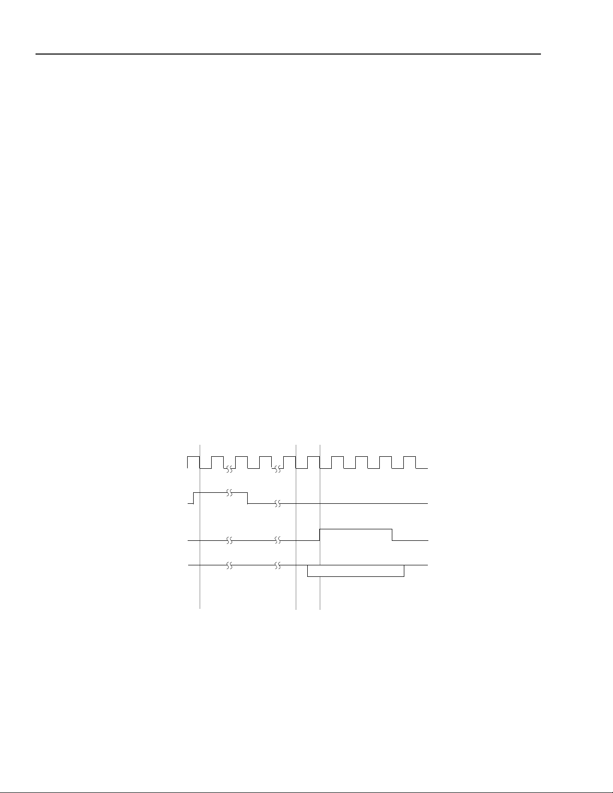
Data Sheet
DSP16210 Digital Signal Processor July 2000
Hardware Architecture
Interrupts and Trap
(continued)
(continued)
INT[3:0] and TRAP Pins
The DSP16210 provides four interrupt pins INT[3:0].
TRAP is a bidirectional pin. At reset TRAP is configured as an input to the processor. Asserting the TRAP
pin forces a pin trap. The trap mechanism is used to
rapidly gain control of the processor for asynchronous
time-critical event handling (typically for catastrophic
error recovery). A separate vector, PTRAP, is provided
for the pin trap (see Table 4 on page 21). Traps cannot
be disabled.
Referring to the timing diagram in Figure 3, the INT[3:0]
or TRAP pin is asserted for a minimum of two cycles.
The pin is synchronized and latched on the next falling
edge of CLK. A minimum of four cycles later, the interrupt or trap gains control of the core and the core
branches to the interrupt service routine (ISR) or trap
service routine (TSR). The actual number of cycles
until the interrupt or trap gains control of the core
depends on the number of wait-states incurred by the
interrupted or trapped instruction. The DSP16210
drives a value (see Table 4 on page 21) onto the
VEC[3:0] pins and asserts the IACK pin.
Low-Power Standby Mode
The DSP16210 has a power-saving standby mode in
which the internal core clock stretches indefinitely until
the core receives an interrupt or trap request. A minimum amount of core circuitry remains active in order to
process the incoming interrupt. The clocks to the
peripherals are unaffected and the peripherals continue to operate during standby mode. The program
places the core in standby mode by setting the AWAIT
bit (bit 15) of the
alf
register (
alf
= 0x8000). After the
AWAIT bit is set, one additional instruction is executed
before the standby mode is entered. When an interrupt
occurs, core hardware resets AWAIT, and normal core
processing is resumed.
The MIOUs remain operational even in standby mode.
Their clocks remain running and they continue any
DMA activity.
nop
Two
AWAIT bit is set. The first
instructions should be programmed after the
nop
(one cycle) is executed
before sleeping; the second is executed after the interrupt signal awakens the DSP and before the interrupt
service routine is executed.
Power consumption can be further reduced by activating other available low-power modes. See Power Man-
agement beginning on page 61 for information on
these other modes.
†
CKO
INT[3:0]/TRAP
† CKO is programmed to be CLK.
‡ The INT[3:0] or TRAP pin must be held high for a minimum of two cycles.
Notes:
A. The DSP16210 synchronizes and latches the INT[3:0] or TRAP.
B. A minimum four-cycle delay before the core services the interrupt or trap (ex ecutes instructions starting at the vector location). For a trap, the
core executes a maximum of three instructions before it services the trap.
‡
IACK
VEC[3:0]
ABC
Figure 3. INT[3:0] and TRAP Timing
24
DRAFT COPY
Lucent Technologies Inc.
Data Sheet
July 2000 D SP16210 Digital Signal Processor
Hardware Architecture
(continued)
Memory Maps
Figure 5 shows the DSP16210 X-memory space memory map (XMAP). Figure 6 on page 26 shows the DSP16210
Y-memory space memory maps (YMAP0 and YMAP1). Instructions differentiate between the X- and Y-memory
spaces by the addressing unit (i.e., the set of pointers) used for the access and not by the physical memory
accessed. Although the memories are 16-bit word-addressable, data or instruction widths can be either 16 bits or
32 bits and the internal memories can be accessed 32 bits at a time. The internal DPRAM is organized into even
and odd interleaved banks as shown in Figure 4. The core data buses (XDB and YDB) are 32 bits wide, so the core
can access 32-bit DPRAM data that has an aligned (even) address in a single cycle.
11 LSBs
OF
ADDRESS
0x000
0x002
EVEN BANK ODD BANK
16 bits 16 bits
32 bits
11 LSBs
OF
ADDRESS
0x001
0x003
0x7FF0x7FE
DPRAM MODULE
1K x 32 bits
(2 Kwords)
0x00000
.... ...
0x0EFFF
0x1FFC0
0x1FFFD
0x20000
.......
0x21FFF
0x80000
........
0x8FFFF
Figure 4. Interleaved Internal DPRAM
XMAP (16 bits)
MEMORY SEGMENT
DPRAM
60 Kwords
RESERVED
CACHE
62 words
RESERVED
IROM 8 Kwords
(RESET AND SYSTEM TRAP
VECTORS; HDS AND BOOT
CODE)
RESERVED
EROM
(64 Kwords)
RESERVED
†
0x0F000
0x1FFBF
0x1FFFE
0x1FFFF
0x22000
...........
0x7FFFF
0x90000
............
16 bits
† These locations are modularly mapped into the previous segment (EROM). For example, location 0xA0000 maps to location 0x80000.
0xFFFFF
Figure 5. X-Memory Space Memory Map
Lucent Technologies Inc.
DRAFT COPY
25
Data Sheet
DSP16210 Digital Signal Processor July 2000
Hardware Architecture
Memory Maps
0x00000
.... ...
0x0EFFF
0x1FFC0
0x1FFFD
0x80000
....
0x8FFFF
0xA0000
....
0xAFFFF
0xC0000
0xC03FF
0xD0000
0xD03FF
0xE0000
0xE003F
0xF0000
....
0xFFFFF
(continued)
YMAP0 (16 bits) YMAP1 (16 bits)
MEMORY SEGMENT
ioc[WEROM] = 0
DPRAM
60 Kwords
RESERVED
CACHE
62 words
RESERVED
ERAMLO
(64 Kwords)
ERAMHI
(64 Kwords)
IO
(64 Kwords)
RESERVED
IORAM0
(1 Kword)
RESERVED
(63 Kwords)
IORAM1
(1 Kword)
RESERVED
(63 Kwords)
(64 words)
RESERVED
(65,504 words)
RESERVED
†
†
†
ESIO
16 bits 16 bits
(continued)
‡
‡
‡
‡
‡
0x0F000
0x1FFBF
0x1FFFE
.........................................
0x7FFFF
0x90000
....
0x9FFFF
0xB0000
....
0xBFFFF
0xC0400
0xCFFFF
0xD0400
0xDFFFF
0xE0040
0xEFFFF
0x00000
.... ...
0x0EFFF
0x1FFC0
0x1FFFD
0x80000
....
0x8FFFF
0xA0000
....
0xAFFFF
0xC0000
0xC03FF
0xD0000
0xD03FF
0xE0000
0xE003F
0xF0000
....
0xFFFFF
MEMORY SEGMENT
ioc[WEROM] = 1
DPRAM
60 Kwords
RESERVED
CACHE
62 words
RESERVED
EROM
(64 Kwords)
RESERVED
(64 Kwords)
RESERVED
IORAM0
(1 Kword)
RESERVED
(63 Kwords)
IORAM1
(1 Kword)
RESERVED
(63 Kwords)
ESIO
(64 words)
RESERVED
(65,504 words)
RESERVED
‡
IO
‡
†
‡
†
‡
†
‡
‡
0x0F000
0x1FFBF
0x1FFFE
...................................... ...
0x7FFFF
0x90000
....
0x9FFFF
0xB0000
....
0xBFFFF
0xC0400
0xCFFFF
0xD0400
0xDFFFF
0xE0040
0xEFFFF
† IORAM0, IORAM1, and ESIO are internal physical memory spaces that are managed by the EMI and are mapped to external memory
addresses.
‡ These locations are modularly mapped into the previous segment. For example, locations 0xD0400—0xD07FF map to locations
0xD0000—0xD03FF and location 0xE0040 maps to location 0xE0000.
Figure 6. Y-Memory Space Memory Maps
The external memory data bus (DB) and the EMI data bus (EDB) are 16 bits wide, and therefore, 32-bit accesses
to external memory and IORAM are broken into two 16-bit accesses.
26
DRAFT COPY
Lucent Technologies Inc.

Data Sheet
July 2000 D SP16210 Digital Signal Processor
Hardware Architecture
Memory Maps
The addresses shown in Figures 5 and 6 correspond to
the 20-bit core address buses (XAB for the XMAP and
YAB for YMAP0/YMAP1). For external memory
accesses, these 20-bit addresses are truncated to
16 bits and the external enable pins (EROM, ERAMHI,
ERAMLO, and IO) differentiate the 64K segment being
accessed. For IORAM accesses, these 20-bit
addresses are truncated to 10 bits.
Boot from External ROM
The EXM pin determines from which memory region
(EROM or IROM) the DSP16210 executes code following a device reset. EXM is captured by the rising edge
of RSTB. If the captured value of EXM is one, the
DSP16210 boots from external ROM (EROM—core
address 0x80000). Otherwise, the DSP16210 boots
from internal IROM (core address 0x20000). See
DSP16210 Boot Routines beginning on page 126 for
details on booting from IROM.
(continued)
(continued)
access to the IORAM and ESIO storage. The EMI automatically translates 32-bit XDB/YDB accesses into two
16-bit DB/EDB accesses and vice versa. If an instruction accesses EMI storage from both the X side and Y
side, the EMI performs the X access first followed by
the Y access and the core incurs a conflict wait-state.
The EMI accesses four external memory segments—
ERAMHI, ERAMLO, EROM, and IO.
Two control registers are encoded by the user to define
or
or
mwait
mwait
mwait
ioc
and avail-
update
the operation of the EMI. Bits 14—0 in
(Table58onpage101) and bits 10 and 7—0 in
(Table54onpage99) apply to the EMI. These pro-
grammable features give the designer flexibility in
choosing among various external memories.
Latency for Programming mwait and ioc Registers
There is a two instruction cycle latency between an
instruction that updates either
ability of the new value in the EMI. It is recommended
that two
external memory) follow each
instruction. See the example below:
nop
s (or other instructions that do not access
ioc
ioc
Data Memory Map Selection
The DSP16210 data memory map selection is based
on the value of the WEROM field (bit 4) in the
ter (Table 54 on page 99). If WEROM is set to 0, the
YMAP0 data memory map is selected. If WEROM is
set to 1, the YMAP1 data memory map is selected. If
WEROM is 1, all ERAMLO accesses are redirected to
the EROM segment.
ioc
regis-
External Memory Interface (EMI)
The external memory interface (EMI) manages off-chip
memory and on-chip IORAM memory and ESIO storage, collectively referred to as EMI storage.
The EMI multiplexes the two sets of core buses
(XAB/XDB and YAB/YDB) onto a single set of external
buses—a 16-bit address bus (AB) and 16-bit data bus
(DB). It also multiplexes the two sets of core buses
onto a single set of internal EMI buses—a 10-bit
address bus (EAB) and a 16-bit data bus (EDB)—for
mwait=0x0222/* Modify mwait */
2*nop /* Wait for latency */
a0=*r0 /* OK to perform EMI read */
For write operations the EMI buffers the data (see
Functional Timing beginning on page 29), software
must verify that all pending external write operations
have completed before modifying
mwait
. Software ensures that all memory operations
have completed by ex ecuting an external memory read
operation. After the read operation is completed, it is
ioc
safe to modify
below for an example:
*r1++=a1 /* EMI write. */
a0=*r2 /* Dummy EMI read. */
mwait=0x0222/* Safe to modify mwait. */
2*nop /* Wait for mwait latency. */
Note:
For the EMI to function properly, the application
program
presented above.
mwait
or
must
adhere to the latency restrictions
ioc
or
. See the code segment
Lucent Technologies Inc.
DRAFT COPY
27

Data Sheet
DSP16210 Digital Signal Processor July 2000
Hardware Architecture
External Memory Interface (EMI)
Programmable Access Time
For each of the four external memory segments, the number of cycles to assert the enable can be selected in
mwait
(Table 58 on page 101). Within
enable for the IO segment, the Y ATIM[3:0] field specifies the number of cycles to assert the enable for the ERAMLO
and ERAMHI segments, and the XATIM[3:0] field specifies the number of cycles to assert the enable for the EROM
segment. On device reset, all access time values are initialized to 15 (
External memory accesses cause the core to incur wait-states. Table 8 on page 28 defines the duration of an
access and the number of wait-states incurred as a function of the programmed access time (IATIM[3:0],
YATIM[3:0], or XATIM[3:0] abbreviated as A). For example, if YATIM[3:0] = 0xB (decimal 11), then the ERAMLO
and ERAMHI enables are asserted for 11 CLK cycles, any accesses to ERAMLO or ERAMHI require 12 CLK
cycles, and the number of wait-states incurred by the core is 12 for read operations and up to and including 12 for
write operations.
Wait-states for write operations can be transparent to the core if subsequent instructions do not access external
memory.
Table 8. Access Time and Wait-States
Number of CLK Cycles
the Enable Pin Is Asserted
Quantity
Range
IATIM[3:0], YATIM[3:0], or XATIM[3:0]
(abbreviated as ATIM)
(continued)
(continued)
mwait
, the IATIM[3:0] field specifies the number of cycles to assert the
mwait
resets to 0x0FFF).
Duration of
Access
ATIM + 1 ATIM + 1 up to and including ATIM + 1
1—15 2—16 2—16 0—16
Read Write
Wait-States Incurred
READY Pin Enables
For each of the four external memory segments,
disable the READY pin. Setting the RDYEN2 bit enables READY for the IO segment, setting the RDYEN1 bit
enables READY for the ERAMLO and ERAMHI segments, and setting the RDYEN0 bit enables READY for the
EROM segment. On device reset, the RDYEN[2:0] bits are cleared, causing the DSP16210 to ignore the READY
pin by default.
Enable Delays
The leading edge of an enable can be delayed to avoid a situation in which two devices drive the data bus
simultaneously . If the leading edge of an enable is delayed, it is guaranteed to be asserted after the RWN signal is
asserted.
Setting DENB2 of
cycle of CLK. Similarly, setting DENB1 delays the leading edge of the ERAM, ERAMHI, and ERAMLO enables,
and setting DENB0 delays the leading edge of the EROM enable. On device reset, the DENB[2:0] bits are cleared,
causing no delay by default.
Memory Map Selection
The WEROM field (
YMAP1 is selected and all ERAMLO accesses are mapped to EROM. This allows the EROM segment, which is
normally read-only, to be written. For example, a program could download code or coefficients into the EROM segment for later use. If WEROM is set, the DENB1 field (
bits 13 and 7—4) control Y-side accesses to EROM.
ioc
(Table 54 on page 99) delays the leading edge of the IO enable by approximately one half-
ioc
bit 4) selects either YMAP0 or YMAP1 (see Figure 6 on page 26 ). If WEROM is set,
mwait
(Table58onpage101) can be programmed to enable or
ioc
bit 1) and the RDYEN1 and YATIM[3:0] fields (
mwait
28
DRAFT COPY
Lucent Technologies Inc.

Data Sheet
July 2000 D SP16210 Digital Signal Processor
Hardware Architecture
External Memory Interface (EMI)
(continued)
(continued)
RWN Advance
The RWNADV field (
ioc
bit 3) controls the amount of delay from the beginning of a write access to the lowering of
the RWN pin. See External Memory Interface under Timing Characteristics and Requirements for details.
CKO Pin Configuration
The CKOSEL[2:0] field (
ioc
bits 7—5) configures the CKO pin as either the internal free-running clock (CLK), the
internal free-running clock held high during low-power standby mode, the output of the CKI input buffer, logic zero,
or logic one. See Table 54 on page 99.
Write Data Drive Delay
The write data delay (WDDLY) field (
ioc
bit 10) controls the amount of time that the EMI delays driving write data
onto the data bus (DB[15:0]). If WDDLY is cleared, the EMI drives the data bus approximately one half-cycle of
CLK after the beginning of the access
of CLK after the beginning of the access
1
. If WDDLY is set, the EMI drives the data bus approximately one full cycle
1
. As a result, setting WDDLY provides an additional delay of one halfcycle for slower external memory. This additional delay is particularly useful if the external memory’s enable is
delayed (the corresponding DENB[2:0] bit is set).
If WDDLY is set, both the turn-on and turn-off delays for the data bus are increased
2
. Because the turn-off delay is
increased, it may be necessary to set the corresponding DENB[2:0] bit for any segments that are read immediately
after writing .
Functional Timing
The following definitions apply throughout:
Low
—an electrical level near ground corresponding to logic zero.
High
—an electrical level near V
Assertion
Deassertion
EMI Storage
—the changing of a signal to its active value.
—the changing of a signal to its inactive value.
—storage that the EMI manages consisting of external memory, IORAM memory, and ESIO memory-
DD
corresponding to logic one.
mapped registers.
EMI Instruction
Non-EMI Instruction
CLK Period
—a DSP16210 instruction that accesses (reads or writes) EMI storage.
—a DSP16210 instruction that does not access EMI storage.
—the time from rising edge to rising edge of the CLK clock; the duration of one single instruction
cycle. All EMI events occur on the rising edge of CLK. It is assumed that the CKO pin is programmed as CLK and
the remainder of this section uses the terms CLK and CKO interchangeably.
1. The beginning of the access occurs when the EMI drops RWN.
2. The data bus active interval is constant regardless of WDDLY.
Lucent Technologies Inc.
DRAFT COPY
29

Data Sheet
DSP16210 Digital Signal Processor July 2000
Hardware Architecture
External Memory Interface (EMI)
Functional Timing
(continued)
(continued)
(continued)
All DSP16210 external memory read and write operations consist of two parts:
Active Part
1.
: Lasts for the number of cycles programmed in the
mwait
register (IATIM[3:0], XATIM[3:0], or
YATIM[3:0]). Begins on a rising edge of CLK (CKO). Immediately after this rising edge:
a.The DSP16210 asserts the memory segment enable. If the leading edge of the memory segment enable is
delayed (the corresponding DENB[2:0] bit of
ioc
is set), the DSP16210 asserts the memory segment enable
one-half of a CLK period later.
b.The DSP16210 places the address on the address bus AB[15:0].
c. RWN becomes valid (high for a read, low for a write).
d.For a read operation, the DSP16210 3-states its data bus DB[15:0] drivers. For a write operation, the
DSP16210 delays driving the data bus by an interval determined by the WDDLY field (
ioc
bit 10). If
WDDLY = 0, the delay is approximately one half-cycle of CLK after RWN goes low. If WDDLY = 1, the delay is
approximately one cycle of CLK after RWN goes low.
Finish Part
2.
: Lasts for one cycle. Begins on a rising edge of CLK (CKO). Immediately after this rising edge:
a.The DSP16210 deasserts the memory segment enable.
b.For a read operation, the DSP16210 latches the data from DB[15:0]. For a write operation, the DSP16210 con-
tinues to drive data onto the data bus for an interval determined by the WDDLY field (
ioc
bit 10). If WDDLY = 0,
the DSP16210 drives the bus for approximately one half-cycle of CLK after the beginning of the finish part. If
WDDLY = 1, the DSP16210 drives the bus for appro ximately one cycle of CLK after the beginning of the finish
part.
As a consequence of the finish part of each memory operation, contention problems caused by back-to-back
assertion of different enables (one instruction with dual accesses) are avoided. Following the finish part, the
DSP16210 continues to drive the address bus with the last valid address until the beginning of the next external
read or write operation.
If an instruction
instruction is
where:
If an instruction
incurred by the core during execution of the second
where:
1. Including possible instruction fetch.
2. Wait-states are incurred by the following instruction and not by the current instruction because the EMI internally buffers write data. In other
words, the core does not wait (as it does in the DSP1620) until the write data has been transferred to EMI storage. Instead, the core continues execution while the EMI waits to transfer the data to EMI storage on the next available memory cycle. A subsequent access to EMI storage causes the core to wait until the prior write operation’s data has been transferred to storage.
reads
from EMI storage, the number of wait-states incurred by the core during execution of that
R.R
is computed as:
R = RX + R
X
R
=Number of wait-states incurred from reading external X-memory1.
Y
R
=Number of wait-states incurred from reading external Y-memory, IORAM memory, or ESIO register.
W
= Number of wait-states incurred from writing external Y-memory, IORAM memory, or ESIO register.
Y
writes
to EMI storage and is immediately followed by a second EMI instruction, wait-states are
2
instruction. The number of wait-states is W:
30
DRAFT COPY
Lucent Technologies Inc.
 Loading...