

AGERE DSP1620 Datasheet
Advisory
May 1999
Clarification to the Serial I/O Control Register
Description for the DSP1620/27/28/29 Devices
Active Clock Frequency
The purpose of this advisory is to clarify the function of the serial I/O control registers in the DSP1620/27/28/29
devices. Specifically, it clarifies the function of the control register field that specifies the active clock frequency .
The device data sheets state that the active clock frequency is a ratio of the
pin (DSP1627/28/29 devices) or the output clock frequency on the CKO pin (DSP1620 device). For all four
devices, the actual active clock frequency is a ratio of the
as either the input clock frequency on the CKI pin or the output of an internal clock synthesizer (PLL).
Table 1 summarizes information for each of the four devices. It lists the document number for each device data
sheet. For example, the data sheet for the DSP1620, entitled
ment number DS97-321WDSP. Table 1 also lists the name of each serial I/O unit on each device, the corresponding control register, the data sheet page number that describes the register, and the corresponding field
within the register that specifies the active clock frequency. For e xample, the DSP1620 contains two serial I/O
units named SIO and SSIO. The control register for SIO is
Bits 8—7 within
sioc
(CLK1 field) specify the active clock frequency of the SIO.
internal
clock frequency, which can be programmed
DSP1620 Digital Signal Processor
sioc
described on page 94 of the data sheet.
input
clock frequency on the CKI
, has the docu-
Table 1. Data Sheet and Serial I/O Information for the DSP1620/27/28/29 Devices
Device Data Sheet
Document Number
DSP1620 DS97-321WDSP SIO
DSP1627 DS96-188WDSP SIO
DSP1628 DS97-040WDSP SIO
DSP1629 DS96-039WDSP SIO
Table 2 shows a corrected description of the CLK/CLK1/CLK2 field of the serial I/O control register. The
specific correction is shown in bold type—the active clock frequency is a ratio of f
Table 2. Corrected Description of CLK/CLK1/CLK2 Field
Field Value Description
CLK
CLK1
CLK2
Active clock frequency =
00
01
Active clock frequency =
10
Active clock frequency =
11
Active clock frequency =
Name Control
Register
sioc
SSIO
SIO2
SIO2
SIO2
SSIOC
sioc
sioc
sioc
f
internal clock
f
internal clock
f
internal clock
f
internal clock
Serial I/O Units
Data Sheet
Page No.
94 8—7 CLK1
96 8—7 CLK2
45 8—7 CLK
55 8—7 CLK
46 8—7 CLK
÷ 2
÷ 6
÷ 8
÷ 10
Active Clock Frequency
Control Field
Bits Name
internal clock
, not of CKI or CKO.
DRAFT COPY

For additional information, contact your Microelectronics Group Account Manager or the following:
INTERNET:
E-MAIL:
N. AMERICA: Microelectronics Group, Lucent Tech nologies Inc., 555 Union Boulevard, Room 30L-15P-BA, Allentown, PA 1 81 03
ASIA PACIFIC: Microelectronics Group, Lucent Technologies Singap ore Pte. Ltd., 77 Science Park Drive, #03-18 Cintech III, Singapore 118256
CHINA: Microelectr on ic s G r ou p, Lucent Technologies (China) Co., Ltd., A-F2, 23/F, Zao Fong Uni verse Buildin g, 1800 Zhong Shan Xi Ro ad, Shanghai
JAPAN: Microelectronics Group, Lucent Technologies Japan Ltd., 7-18, Higashi-Gotanda 2-chome, Shinagawa-ku, Tokyo 141, Japan
EUROPE: Data Requests: MICROELECTRONICS GROUP DATALINE:
Lucent Technologies Inc. reserves the right to make changes to the product(s) or information contained herein without notice. No liability is assumed as a result of their use or application. No
rights under any patent accompany the sale of any such product(s) or information.
http://www.lucent.com/micro
docmaster@micro.lucent.com
1-800-372-2447
Tel. (65) 778 8833
200233 P. R. China
Tel. (81) 3 5421 1600
Techni cal Inquiries: GERMANY:
, FAX 610-712-4106 (In CANADA:
, FAX (65) 777 7495
Tel . ( 86) 21 6440 0468, ext. 316
, FAX (81) 3 5421 1700
FRANCE:
(39) 02 6608131
ITAL Y:
(49) 89 95086 0
(33) 1 40 83 68 00
(Milan), SPAIN:
1-800-553-2448
, F A X ( 86) 21 6440 0652
(Munich), UNITED KINGDOM:
(Paris), SWEDEN:
, FAX 610-712-4106)
Tel. (44) 1189 324 299
(46) 8 594 607 00
(34) 1 807 1441
(Madrid)
, FAX (44) 1189 328 148
(44) 1344 865 900
(Stockholm), FINLAND:
(Ascot),
(358) 9 4354 2800
(Helsinki),
Copyright © 1999 Lucent Technologies Inc.
All Rights Reserved
May 1999
AY99-001WDSP
(must accompany DS97-321WDSP, DS96-188WDSP, DS97-040WDSP, and DS96-039WDSP)

Data Sheet
June 1998
DSP1620 Digital Signal Processor
1 Features
„ Optimized for digita l cellu lar inf rastruct ure appl icatio ns—
equalization, channel coding, speech coding
„ Large, on-chip DPRAM (32 Kwords) that eliminates
need for fast external SRAM
„ ECCP for efficient equalization and channel coding
„ DMA-based I/O that m inimizes DSP core overhead for
I/O processing
„ Bit manipulation unit for higher coding efficiency
„ On-chip programmable, PLL (phase-lock loop) clock
synthesizer enables low-cost, low -power implementations
„ Instruction cycle times:
—At 3 V are 8.3 ns (120 MIPS), 10.0 ns (100 MIPS),
and 11.1 ns (90 MIPS)
—At 5 V is 11.1 ns (90 MIPS)
„ Low system power consumption with flexible power
management modes
„ Support for 128 Kwords external memory access
„ Four external vectored interrupts
„ 25 Mbits/s serial I/O port (SIO) with multiprocessor
capability—16-bit data channel, 8-bit protocol channel
„ Two dedicated DMA controllers (MIOUs) to off-load I/O
processing from D SP core
„ 25 Mbits/s simple serial I/O port (SSIO) coupled with
MIOU0 to support low-overhead DMA-based I/O
„ 16-bit parallel host interface (PHIF16) coupled with
MIOU1 to support low-overhead DMA-based I/O
—Supports 8- or 16-bit external bus configurations
—Supports 8- or 16-bit logical transfers in 8-bit
external configuration
Motorola
—
„ Memory sequencer for sin gle-in st ruct i on acc ess to both
*
X and Y external memory space
„ Single-cycle squaring feature increases coding efficien-
cy
„ 16 x 16-bit multiplication and 36-bit acc umula t ion i n one
instruction cycle for efficient algorithm implementations
„ Instruction cache for high-speed, program-efficient,
zero-overhead looping
„ 8-bit control I/O interface provides increased flexibility
and lower system costs
„ 256 memory-mapped I/O ports for interfacing flexibility
„
„ Full-speed in-circuit emulation hardware development
‡
IEEE
P1149.1 test port (JTAG with boundary scan)
system on-chip for faster system developments
or
Intel
†
compatible
„ Supported by DSP1620 software and hardware
development tools
„ On-chip boot routines for flexible downloading
„ 132-pin BQFP package and 144-pin TQFP package
2 Description
The DSP1620 is a DSP1600 core-based fixed-point digital
signal processor with a large am ount of on-chip RAM and a
flexible DMA-base d I /O stru ct ure that is designed specifically for digital cellular infrastructure applications. This device
also contains a b it man ipulat ion unit (BMU) and an error correction coprocessor (ECCP) for enhanced signal coding efficiency. The DSP1620 offers 120, 100, or 90 MIPS
performance at 3 V and 90 MIPS performance at 5 V.
The large, 32 Kword on-chip, dual-port RAM (DPRAM) supports downloadable system design—a must for wireless infrastructure—to support field upgrades for evolving digital
cellular standards . Th e DSP162 0 can ad dress 30 Kwords of
on-chip DPRAM an d up to 64 Kwords of external storag e in
its code and coeffic ient memory addr ess spac e. In addition ,
the DSP1620 can address 32 Kwords of on-chip DPRAM
and up to 128 Kwords of external storage in its external
memory address space (64 Kwords/Data and 64 Kwords/
Program).
To optimize I/O throughput and reduce the I/O service routine burden o n the DSP core, the D SP1620 is equip ped with
two modular I/O units (MIOUs) that manage one of the serial
ports (SSIO) and the 16-bit parallel host i nterface (PHIF16)
peripherals. The MIOU s provide trans parent DMA transfe rs
between the peripherals and on-chip DPRAM.
The error cor rect io n coprocessor is a powerful hardwa re engine for Viterbi decoding with instructions for maximum
likelihood sequence estimation (MLSE) equalization and
convolutional decoding.
The combination of a large, on-chip RAM, 120 MIPS performance, and ef fi cien t I/O mana geme nt mak es the DSP1620
an ideal solution for supporting multiple channels of voice
and data traffic in digital cellular infrastructure equipment.
The device is packaged in a 132-pin BQFP and a 144-pin
TQFP; it is available with 11.1 ns instruction cycle speed at
5 V and 8.3 ns, 10 .0 ns, and 11 .1 ns instructi on cycle speeds
at 3 V.
*
Motorola
is a registered trademark of Motorola, Inc.
Intel
is a registered trademark of Intel Corp.
†
IEEE
is a registered trademark of The Institute of Electrical and
‡
Electronics Engineers, Inc.

Data Sheet
DSP1620 Digital Signal Processor June 1998
Table of C o ntent s
Contents Page Contents Page
➤➤➤➤
1 Features............................................................ 1
➤➤➤➤
2 Description........................................................ 1
➤➤➤➤
3 Pin Information.................................................. 9
➤➤➤➤
4 Hardware Architecture.................................... 14
➤
4.1 DSP1620 Architectural Overview...........14
➤
4.2 DSP1600 Core Architectural Overview..20
➤
4.3 Interrupts and Trap.................................23
➤
4.4 Memory Maps and Wait-States..............26
➤
4.5 External Memory Interface (EMI) ...........30
➤
4.6 Bit Manipulation Unit (BMU)...................34
➤
4.7 Serial I/O Unit (SIO)...............................34
➤
4.8 Modular I/O Unit (MIOU) ........................37
➤
4.9 Simple Serial I/O Unit (SSIO).................46
➤
4.10 Parallel Host Interface (PHIF16) ............47
➤
4.11 Bit I/O Unit (BIO) ....................................49
➤
4.12 Timer......................................................49
➤
4.13 Error Correction Coprocessor (ECCP)...50
➤
4.14 Control Register (ECON) .......................58
➤
4.15 JTAG Test Por t ......................................66
➤
4.16 Clock Synthesis......................................68
➤
4.17 Power Management............................... 71
➤➤➤➤
5 Software Architecture ..................................... 77
➤
5.1 Instruction Set........................................77
➤
5.2 Register Settings....................................86
➤
5.3 Reset States...........................................98
➤
5.4 Instruction Set Formats..........................99
➤
5.5 Field Descriptions.................................101
➤➤➤➤
6 Signal Descriptions....................................... 105
➤
6.1 System Interface..................................106
➤
6.2 External Memory Interface...................107
➤
6.3 SIO Interface........................................107
➤
6.4 SSIO Interface......................................108
➤
6.5 PHIF16 Interface..................................109
➤
6.6 Control I/O Interface.............................110
➤
6.7 JTAG Test Interface.............................110
➤➤➤➤
7 DSP1620 Boot Routines............................... 111
➤
7.1 Logical Flow of Events.........................111
➤
7.2 Description of Routines........................114
➤➤➤➤
8 Device Characteristics.................................. 116
➤
8.1 Absolute Maximum Ratings .................116
➤
8.2 Handling Precautions...........................116
➤
8.3 Recommended Operating Conditions..116
➤
8.4 Package Thermal Considerations........117
➤➤➤➤
9 Electrical Characteristics and Requirements 118
➤
9.1 Power Dissipation ................................121
➤➤➤➤
10 Timing Characteristics and Requirements
for 5 V Operation ......................................... 123
➤
10.1 DSP Clock Generation......................... 124
➤
10.2 Reset Circuit.........................................125
➤
10.3 Reset Synchronization.........................126
➤
10.4 JTAG I/O Specifications....................... 127
➤
10.5 Interrupt................................................128
➤
10.6 Bit Input/Output (BIO)...........................129
➤
10.7 External Memory Interface...................130
➤
10.8 PHIF16 Specifications..........................135
➤
10.9 Serial I/O Specifications.......................141
➤
10.10Multiprocessor Communication............146
➤➤➤➤
11 Timing Characteristics and Requirements
for 3 V Operation ......................................... 147
➤
11.1 DSP Clock Generation......................... 148
➤
11.2 Reset Circuit.........................................149
➤
11.3 Reset Synchronization.........................150
➤
11.4 JTAG I/O Specifications....................... 151
➤
11.5 Interrupt................................................152
➤
11.6 Bit Input/Output (BIO)...........................153
➤
11.7 External Memory Interface...................154
➤
11.8 PHIF16 Specifications..........................159
➤
11.9 Serial I/O Specifications.......................165
➤
11.10Multiprocessor Communication............170
➤➤➤➤
12 Outline Diagrams.......................................... 171
➤
12.1 132-Pin BQFP Outline Diagram...........171
➤
12.2 144-Pin TQFP Outline Diagram ...........172
2 Lucent Technologies Inc.

Data Sheet
June 1998 DSP1620 Digital Signal Processor
List of Figures
Figures Page
➤
Figure 1. DSP1620 132-Pin BQFP Pin Diagram (Top View)..........................................................................9
➤
Figure 2. DSP1620 144-Pin TQFP Pin Diagram (Top View) ........................................................................10
➤
Figure 3. DSP1620 Block Diagram...............................................................................................................17
➤
Figure 4. DSP1600 Core Block Diagram ......................................................................................................21
➤
Figure 5. EMI Configuration with 32K x 16 SRAM........................................................................................31
➤
Figure 6. EMI Configuration with 64K x 16 SRAM........................................................................................32
➤
Figure 7. READY Pin Timing Example for
➤
Figure 8. Multiprocessor Communications and Connections........................................................................36
➤
Figure 9. IORAM Configuration for Active MIOU ..........................................................................................39
➤
Figure 10. Error Correction Coprocessor Bl ock..............................................................................................51
➤
Figure 11. DSP Core Operation Sequence ....................................................................................................53
➤
Figure 12. ECCP Operation Sequence...........................................................................................................54
➤
Figure 13. Clock Source Block Diagram.........................................................................................................68
➤
Figure 14. Power Management Using the
➤
Figure 15. DSP1620 Pinout by Interface ......................................................................................................105
➤
Figure 16. Plot of VOH vs. IOH Under Typical Operating Conditions ..........................................................120
➤
Figure 17. Plot of VOL vs. IOL Under Typical Operating Conditions............................................................120
➤
Figure 18. I/O Clock Timing Diagram ...........................................................................................................124
➤
Figure 19. Powerup Reset and Chip Reset Timing Diagram........................................................................125
➤
Figure 20. Reset Synchronization Timing.....................................................................................................126
➤
Figure 21. JTAG Timing Diagram .............................................................................................................127
➤
Figure 22. Interrupt Timing Diagram ...........................................................................................................128
➤
Figure 23. Write Outputs Followed by Read Inputs (
➤
Figure 24. Write Outputs and Test Inputs (
➤
Figure 25. Enable Transition Timing ...........................................................................................................130
➤
Figure 26. External Memory Data Read Timing Diagram ............................................................................131
➤
Figure 27. External Memory Data Write Timing Diagram ...........................................................................132
➤
Figure 28. Write Cycle Followed by Read Cycle .........................................................................................133
➤
Figure 29. READY Extended Read Cycle Timing.........................................................................................134
➤
Figure 30. PHIF16
➤
Figure 31. PHIF16
➤
Figure 32. PHIF16
➤
Figure 33. PHIF16
➤
Figure 34. PHIF16
➤
Figure 35. PHIF16 PIBF and POBE Reset Timing Diagram .......................................................................140
➤
Figure 36. PHIF16 PIBF and POBE Disable Timing Diagram ......................................................................140
➤
Figure 37. SIO Passive Mode Input Timing Diagram ..................................................................................141
➤
Figure 38. SIO Active Mode Input Timing Diagram ...................................................................................142
➤
Figure 39. SIO Passive Mode Output Timing Diagram ................................................................................143
➤
Figure 40. SIO Active Mode Output Timing Diagram....................................................................................144
➤
Figure 41. Serial I/O Active Mode Clock Timing ..........................................................................................145
➤
Figure 42. SIO Multiprocessor Timing Diagram............................................................................................146
➤
Figure 43. I/O Clock Timing Diagram ...........................................................................................................148
➤
Figure 44. Powerup Reset and Chip Reset Timing Diagram ......................................................................149
➤
Figure 45. Reset Synchronization Timing.....................................................................................................150
➤
Figure 46. JTAG Timing Diagram ...............................................................................................................151
➤
Figure 47. Interrupt Timing Diagram ...........................................................................................................152
➤
Figure 48. Write Outputs Followed by Read Inputs (
➤
Figure 49. Write Outputs and Test Inputs (
➤
Figure 50. Enable Transition Timing .........................................................................................................154
➤
Figure 51. External Memory Data Read Timing Diagram ............................................................................155
➤
Figure 52. External Memory Data Write Timing Diagram .............................................................................156
Intel
Mode Signaling (Read and Write) Timing Diagram................................................135
Intel
Mode Signaling (Pulse Period and Flags) Timing Diagram ..................................136
Motorola
Motorola
Intel
Mode Signaling (Read and Write) Timing Diagram .......................................137
Mode Signaling (Pulse Period and Flags) Timing Diagram.............................138
or
Motorola
Mode Signaling (Status Register Read) Timing Diagram ..................139
mwait = 0x0020
powerc
cbit = Immediate
cbit = Immediate
and the
cbit = Immediate; a1 = sbit
cbit = Immediate; a1 = sbit
.........................................................................33
pllc
Registers ....................................................72
) ..................................... 129
) ....................................................................129
) ....................................153
) ....................................................................153
Lucent Technologies Inc. 3

Data Sheet
DSP1620 Digital Signal Processor June 1998
List of Figures
(continued)
Figures Page
➤
Figure 53. Write Cycle Followed by Read Cycle ..........................................................................................157
➤
Figure 54. READY Extended Read Cycle Timing......................................................................................... 158
➤
Figure 55. PHIF16
➤
Figure 56. PHIF16
➤
Figure 57. PHIF16
➤
Figure 58. PHIF16
➤
Figure 59. PHIF16
➤
Figure 60. PHIF16 PIBF and POBE Rese t Timing Diagram ........................................................................164
➤
Figure 61. PHIF16 PIBF and POBE Disable Timing Diagram ......................................................................164
➤
Figure 62. SIO Passive Mode Input Timing Diagram ................................................................................. 165
➤
Figure 63. SIO Active Mode Input Timing Diagram ....................................................................................166
➤
Figure 64. SIO Passive Mode Output Timing Diagram ...............................................................................167
➤
Figure 65. SIO Active Mode Output Timing Diagram ...................................................................................168
➤
Figure 66. SIO Active Mode Clock Timing.................................................................................................... 169
➤
Figure 67. SIO Multiprocessor Timing Diagram............................................................................................170
Intel
Mode Signaling (Read and Write) Timing Diagram ...........................................159
Intel
Mode Signaling (Pulse Period and Flags) Timing Diagram .................................160
Motorola
Motorola
Intel
Mode Signaling (Read and Write) Timing Diagram ........................................161
Mode Signaling (Pulse Period and Flags) Timing Diagram.............................162
or
Motorola
Mode Signaling (Status Register Read) Timing Diagram ...................163
4 Lucent Technologies Inc.

Data Sheet
June 1998 DSP1620 Digital Signal Processor
List of Ta bl e s
Tables Page
➤
Table 1. Pin Descriptions............................................................................................................................... 11
➤
Table 2. DSP1620 Block Diagram Legend ................................................................................................... 18
➤
Table 3. DSP1600 Core Block Diagram Legend ........................................................................................... 22
➤
Table 4. Interrupt Vectors .............................................................................................................................. 24
➤
Table 5. Instruction/Coefficient Memory Maps............................................................................................... 27
➤
Table 6. Data Memory Maps.......................................................................................................................... 29
➤
Table 7. MIOU Commands ............................................................................................................................ 38
➤
Table 8. MIOU Command Latencies.............................................................................................................. 42
➤
Table 9. PHIF16 Output Function.................................................................................................................. 48
➤
Table 10. P HIF16 Input Function..................................................................................................................... 48
➤
Table 11. PSTAT Register............................................................................................................................... 48
➤
Table 12. BIO Operations................................................................................................................................ 49
➤
Table 13. Incremental Branc h Metrics............................................................................................................. 52
➤
Table 14. E CCP Instruction Encoding ............................................................................................................. 55
➤
Table 15. R e set State of ECCP Registers....................................................................................................... 55
➤
Table 16. Mem o ry-M apped Registers ............................................................................................................. 56
➤
Table 17. C ontrol Fields of the Control Register (ECON)................................................................................ 58
➤
Table 18. R epresentative U pdateM LSE Instruc tion Cycles (SH = 0) .............................................................. 64
➤
Table 19. R epresentative U pdateM LSE Instruc tion Cycles (SH = 1) ............................................................. 64
➤
Table 20. R epresentative U pdateConv Ins truc tion Cyc les (S H = 0) ............................................................... 65
➤
Table 21. R epresentative U pdateConv Ins truc tion Cyc les (S H = 1) ............................................................... 65
➤
Table 22. JTAG Instruction Register ................................................................................................................ 66
➤
Table 23. JTAG Boundary-Scan Register........................................................................................................ 67
➤
Table 24. Latency Tim e s for Switching Betw een CKI- and PLL-Based Clocks............................................... 70
➤
Table 25. Multiply/A LU Instruc tions ................................................................................................................. 78
➤
Table 26. R eplacement Table for Mu ltiply/ALU Instruc tions............................................................................ 78
➤
Table 27. R eplacement Table for Special Function Instructions...................................................................... 79
➤
Table 28. R eplacement Table for Control Instructions..................................................................................... 80
➤
Table 29. D SP1620 C onditional Mnemonics ................................................................................................... 81
➤
Table 30. F3 ALU Instructions ......................................................................................................................... 82
➤
Table 31. Replacement Table for F3 A L U Instructions and BM U Instructions................................................. 83
➤
Table 32. R eplacement Table for Cache Instructions...................................................................................... 84
➤
Table 33. R eplacement Table for Data Move Instructions............................................................................... 85
➤
Table 34.
➤
Table 35.
➤
Table 36.
➤
Table 37.
➤
Table 38.ID — JTAG Identification Register................................................................................................... 88
➤
Table 39.
➤
Table 40.
➤
Table 41.
➤
Table 42.
➤
Table 43.
➤
Table 44.
➤
Table 45.
➤
Table 46.
➤
Table 47.
➤
Table 48.
➤
Table 49.
➤
Table 50.
➤
Table 51.
➤
Table 52.
alf
Register ...................................................................................................................................... 86
auc
— Arithmetic Unit Control Register........................................................................................... 87
cbit
— BIO Control Register............................................................................................................ 88
sbit
— BIO Status Register ............................................................................................................. 88
inc
— Interrupt Control Register...................................................................................................... 89
ins
— Interrupt Status Register ....................................................................................................... 89
ioc
— I/O Configuration Register..................................................................................................... 90
mwait
— EMI Configuration Register.............................................................................................. 90
PHIFC
— PHIF16 Control Register ................................................................................................. 91
pllc
— Phase-Locked Loop Control Register .................................................................................. 91
powerc
psw
saddx
sbit
cbit
sioc
srta
SSIOC
— Power Control Register.................................................................................................. 92
— Processor Status Word Register......................................................................................... 92
— Multiprocessor Serial Address/Protocol Register............................................................. 92
— BIO Status Register ............................................................................................................. 93
— BIO Control Register............................................................................................................ 93
— Serial I/O Control Registers ................................................................................................ 94
— Serial Receive/Transmit Address Register.......................................................................... 95
— Simple Serial I/O Control Registers ................................................................................ 96
Lucent Technologies Inc. 5

Data Sheet
DSP1620 Digital Signal Processor June 1998
List of Tables
(continued)
Tables Page
➤
Table 53.
➤
Table 54.
➤
Table 55. Register Settings After Reset .......................................................................................................... 98
➤
Table 56. T Field............................................................................................................................................ 101
➤
Table 57. D Field ........................................................................................................................................... 101
➤
Table 58. aT Field.............................................................................................................. ............................ 101
➤
Table 59. S Field............................................................................................................................................ 101
➤
Table 60. F1 Field.............................................................................................................. ............................ 101
➤
Table 61. X Field............................................................................................................................................ 101
➤
Table 62. Y Field............................................................................................................................................ 102
➤
Table 63. Z Field............................................................................................................................................ 102
➤
Table 64. F2 Field.............................................................................................................. ............................ 102
➤
Table 65. CON Field...................................................................................................................................... 102
➤
Table 66. R Field ........................................................................................................................................... 103
➤
Table 67. B Field............................................................................................................................................ 103
➤
Table 68. DR Field......................................................................................................................................... 103
➤
Table 69. I Field............................................................................................................................................. 103
➤
Table 70. SI Field........................................................................................................................................... 103
➤
Table 71. F3 Field.............................................................................................................. ............................ 104
➤
Table 72. SRC2 Field .................................................................................................................................... 104
➤
Table 73. F4 and AR Fields........................................................................................................................... 104
➤
Table 74. Recommended Operating Conditions ............................................................................................ 116
➤
Table 75. Electrical Characteristics and Requirements................................................................................. 118
➤
Table 76. Electrical Requirements for Mask-Programmable Input Clock Options......................................... 118
➤
Table 77. PLL Electrical Specifications, VCO Frequency Ranges................................................................. 119
➤
Table 78. PLL Electrical Specifications and
➤
Table 79. Power Dissipation and Wake-Up Latency ..................................................................................... 121
➤
Table 80. Timing Requirements for Input Clock ............................................................................................ 124
➤
Table 81. Timing Characteristics for Input Clock and Output Clock .............................................................. 124
➤
Table 82. Timing Requirements for Powerup Reset and Chip Reset ............................................................ 125
➤
Table 83. Timing Characteristics for Powerup Reset and Chip Reset........................................................... 125
➤
Table 84. Timing Requirements for Reset Synchronization Timing............................................................... 126
➤
Table 85. Timing Requirements for JTAG Input/Output ................................................................................ 127
➤
Table 86. Timing Characteristics for JTAG Input/Output ............................................................................... 127
➤
Table 87. Timing Requirements for Interrupt................................................................................................. 128
➤
Table 88. Timing Characteristics for Interrupt................................................................................................ 128
➤
Table 89. Timing Requirements for BIO Input Read...................................................................................... 129
➤
Table 90. Timing Characteristics for BIO Output ........................................................................................... 129
➤
Table 91. Timing Requirements for BIO Input Test ....................................................................................... 129
➤
Table 92. Enable Transition Timing When Memory Enables and RWN Are Not Delayed
➤
Table 93. Timing Characteristics for Delayed External Memory Enables (When
➤
Table 94. Timing Characteristics for External Memory Acces s ..................................................................... 131
➤
Table 95. Timing Requirements for External Memory Read (EROM, ERAMHI, I/O, ERAMLO).................... 131
➤
Table 96. Timing Characteristics for External Memory Data Write (All Enables)........................................... 132
➤
Table 97. Timing Characteristics for Write Cycle Followed by Read Cycle................................................... 133
➤
Table 98. Timing Requirements for READY Extended Read Cycle Timing................................................... 134
➤
Table 99. Timing Requirements for PHIF16
➤
Table 100. Timing Characteristics for PHIF16
➤
Table 101. Timing Requirements for PHIF16
➤
Table 102. Timing Characteristics for PHIF16
➤
Table 103. Timing Requirements for PHIF16
tdms
— Time-Division Multiplex Slot Register................................................................................ 97
timerc
— Timer Control Register .................................................................................................... 97
pllc
Register Settings............................................................... 119
(When
ioc
DENB[4:0] = 0x00 and
ioc
RWNADV = 0x1)............................................................... 130
ioc
DENB[4:0] = 0x1F)..... 130
Intel
Mode Signaling (Read and Write).................................... 135
Intel
Mode Signaling (Read and Write)................................... 135
Intel
Mode Signaling (Pulse Period and Flags)........................ 136
Intel
Mode Signaling (Pulse Period and Flags)....................... 136
Motorola
Mode Signaling (Read and Write)............................. 137
6 Lucent Technologies Inc.

Data Sheet
June 1998 DSP1620 Digital Signal Processor
List of Tables
(continued)
Tables Page
➤
Table 104. Timing Char acteristics for PHIF16
➤
Table 105. Timing Requirements for PHIF16
➤
Table 106. Timing Char acteristics for PHIF16
➤
Table 107. Timing Requirements for
➤
Table 108. Timing Char acteristics for
➤
Table 109. PHIF16 Timing Characteristics for PIBF and POBE Reset............................................................ 140
➤
Table 110. PHIF16 Timing Characteristics for PIBF and POBE Disable......................................................... 140
➤
Table 111. Timing Requirements for Serial Inputs (Passive Mode)................................................................. 141
➤
Table 112. Timing Characteristics for Serial Outputs (Passive Mode) ............................................................ 141
➤
Table 113. Timing Requirements for Serial Inputs (Active Mode) ................................................................... 142
➤
Table 114. Timing Characteristics for Serial Outputs (Active Mode)............................................................... 142
➤
Table 115. Timing Requirements for Serial Inputs (Passive Mode)................................................................. 143
➤
Table 116. Timing Characteristics for Serial Outputs (Passive Mode) ............................................................ 143
➤
Table 117. Timing Characteristics for Serial Outputs ...................................................................................... 144
➤
Table 118. Timing Characteristics for Signal Generation ................................................................................ 145
➤
Table 119. Timing Requirements for SIO Multiprocessor Communication...................................................... 146
➤
Table 120. Timing Characteristics for SIO Multiprocessor Communication..................................................... 146
➤
Table 121. Timing Requirements for Input Clock............................................................................................. 148
➤
Table 122. Timing Characteristics for Input Clock and Output Clock .............................................................. 148
➤
Table 123. Timing Requirements for Powerup Reset and Chip Reset ............................................................ 149
➤
Table 124. Timing Characteristics for Powerup Reset and Chip Reset........................................................... 149
➤
Table 125. Timing Requirements for Reset Synchronization Timing............................................................... 150
➤
Table 126. Timing Requirements for JTAG Input/Output................................................................................. 151
➤
Table 127. Timing Characteristics for JTAG Input/Output ............................................................................... 151
➤
Table 128. Timing Requirements for Interrupt................................................................................................. 152
➤
Table 129. Timing Characteristics for Interrupt................................................................................................ 152
➤
Table 130. Timing Requirements for BIO Input Read...................................................................................... 153
➤
Table 131. Timing Characteristics for BIO Output........................................................................................... 153
➤
Table 132. Timing Requirements for BIO Input Test ....................................................................................... 153
➤
Table 133. Enable Transition Timing When Memory Enables and RWN Are Not Delayed
(When
➤
Table 134. Timing Char acteristics for Delayed External Memory Enables (When
➤
Table 135. Timing Characteristics for External Memory Access ..................................................................... 155
➤
Table 136. Timing Requirements for External Memory Read (EROM, ERAMHI, I/O, ERAMLO).................... 155
➤
Table 137. Timing Characteristics for External Memory Data Write (All Enables)........................................... 156
➤
Table 138. Timing Characteristics for Write Cycle Followed by Read Cycle................................................... 157
➤
Table 139. Timing Requirements for READY Extended Read Cycle Timing................................................... 158
➤
Table 140. Timing Requirements for PHIF16
➤
Table 141. Timing Char acteristics for PHIF16
➤
Table 142. Timing Requirements for PHIF16
➤
Table 143. Timing Char acteristics for PHIF16
➤
Table 144. Timing Requirements for PHIF16
➤
Table 145. Timing Char acteristics for PHIF16
➤
Table 146. Timing Requirements for PHIF16
➤
Table 147. Timing Char acteristics for PHIF16
➤
Table 148. Timing Requirements for PHIF16
➤
Table 149. Timing Char acteristics for PHIF16
➤
Table 150. PHIF16 Timing Characteristics for PIBF and POBE Reset............................................................ 164
➤
Table 151. PHIF16 Timing Characteristics for PIBF and POBE Disable......................................................... 164
➤
Table 152. Timing Requirements for Serial Inputs (Passive Mode)................................................................. 165
➤
Table 153. Timing Characteristics for Serial Outputs (Passive Mode) ............................................................ 165
➤
Table 154. Timing Requirements for Serial Inputs (Active Mode) ................................................................... 166
ioc
DENB[4:0] = 0x00 and
Intel
Intel
and
and
Motorola
Motorola
Motorola
Motorola
Motorola
ioc
Intel
Intel
Intel
Intel
Motorola
Motorola
Motorola
Motorola
Intel
Intel
Mode Signaling (Read and Write)............................ 137
Mode Signaling (Pulse Period and Flags)................. 138
Mode Signaling (Pulse Period and Flags)................ 138
Mode Signaling (Status Register Read) .................. 139
Mode Signaling (Status Register Read)................. 139
RWNADV = 0x1)............................................................... 154
ioc
DENB[4:0] = 0x1F) ..... 154
Mode Signaling (Read and Write) .................................... 159
Mode Signaling (Read and Write)................................... 159
Mode Signaling (Pulse Period and Flags)........................ 160
Mode Signaling (Pulse Period and Flags) ....................... 160
Mode Signaling (Read and Write)............................. 161
Mode Signaling (Read and Write)............................ 161
Mode Signaling (Pulse Period and Flags)................. 162
Mode Signaling (Pulse Period and Flags)................ 162
and
and
Motorola
Motorola
Mode Signaling (Status Register Read)..... 163
Mode Signaling (Status Register Read).... 163
Lucent Technologies Inc. 7

Data Sheet
DSP1620 Digital Signal Processor June 1998
List of Tables
(continued)
Tables Page
➤
Table 155. Timing Characteristics for Serial Outputs (Active Mode) ............................................................... 166
➤
Table 156. Timing Requirements for Serial Inputs (Passive Mode)................................................................. 167
➤
Table 157. Timing Characteristics for Serial Outputs (Passive Mode) ............................................................ 167
➤
Table 158. Timing Characteristics for Serial Output (Active Mode)................................................................. 168
➤
Table 159. Timing Characteristics for Signal Generation ................................................................................ 169
➤
Table 160. Timing Requirements for SIO Multiprocessor Communication...................................................... 170
➤
Table 161. Timing Characteristics for SIO Multiprocessor Comm unication..................................................... 170
8 Lucent Technologies Inc.
Data Sheet
June 1998 DSP1620 Digital Signal Processor
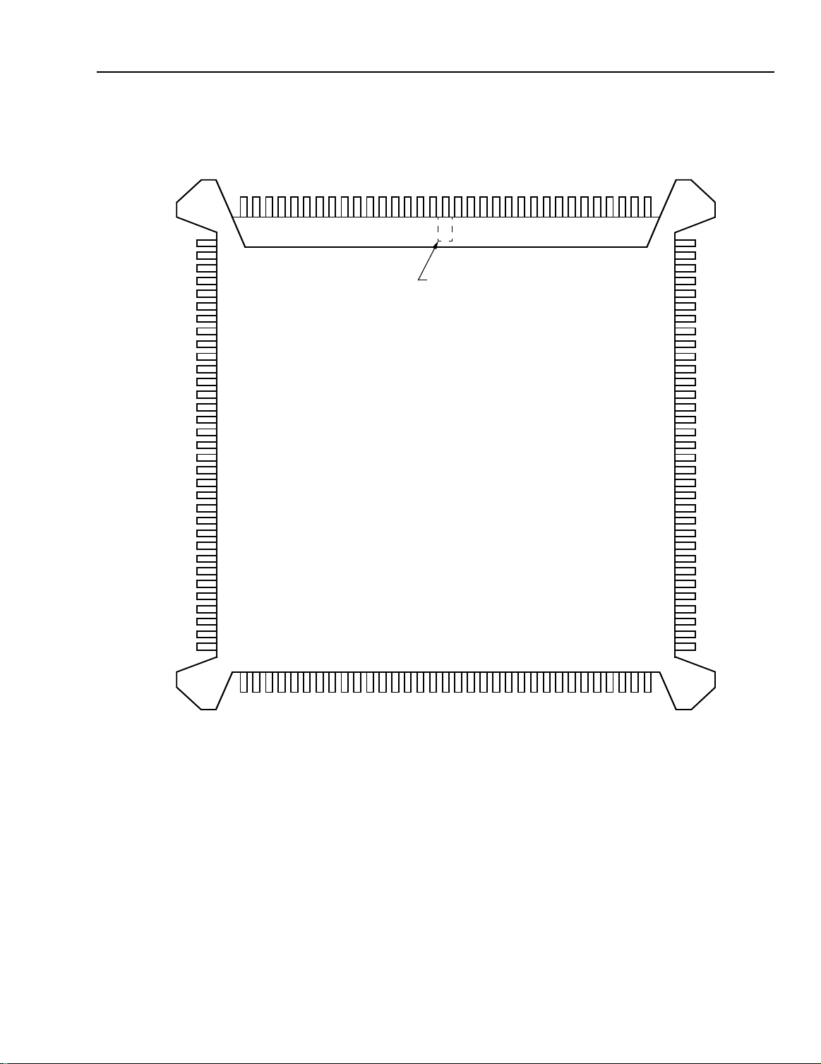
3 Pin Information
V
SSA
CKI
V
DDA
TDI
TDO
TMS
TCK
TRST
INT3
INT2
INT1
INT0
IACK
TRAP
V
DD
CKO
V
RSTB
STOP
READY
VEC0/IOBIT7
VEC1/IOBIT6
VEC2/IOBIT5
VEC3/IOBIT4
V
DD
IOBIT3
IOBIT2
IOBIT1
IOBIT0
DOEN2
DO2
OLD2
V
SS
AB2
AB1
AB0
V
15
16171413121110
18
19
20
21
22
23
24
25
26
27
28
29
30
31
32
33
SS
34
35
36
37
38
39
40
41
42
43
44
45
46
47
48
49
SS
50
53
52
51
5455565758596061626364656667686970717273747576777879808182
AB6
AB5
AB4
VDDAB3
987654321
AB9
AB8
VSSAB7
AB12
VDDAB11
AB10
PIN #1
IDENTIFIER
ZONE
DSP1620
132-PIN BQFP
VSSAB15
AB14
AB13
132
131
130
129
EXM
128
EROM
RWN
127
126
ERAMLO
125
ERAMHI
VDDERAMXIODB0
124
123
122
121
SS
DB1
DB2
V
119
118
117
120
116
115
114
113
112
111
110
109
108
107
106
105
104
103
102
101
100
83
V
DD
DB3
DB4
DB5
DB6
V
SS
DB7
DB8
DB9
DB10
V
DD
DB11
DB12
DB13
DB14
DB15
V
99
98
97
96
95
94
93
92
91
90
89
88
87
86
85
84
SS
OBE1
IBF1
DI1
ILD1
ICK1
OCK1
V
DD
OLD1
DO1
SYNC1
SADD1
DOEN1
PIDS
PCSN
PSTAT
V
SS
DD
V
ICK2
OCK2
OBE2
PB15
SS
DI2
V
IBF2
ILD2
DD
V
PB12
PB13
PB14
PB11
SS
V
PB7
PB8
PB9
PB10
PB6
PB5
PB4
DD
V
PB3
PB2
PB1
PB0
SS
V
POBE
PIBF
PODS
DD
V
PBSEL
5-4773(F)
Figure 1. DSP1620 132-Pin BQFP Pin Diagram (Top View)
Lucent Technologies Inc. 9

Data Sheet
DSP1620 Digital Signal Processor June 1998
3 Pin Information
NU*
CKI
TDI
TDO
TMS
TCK
INT3
INT2
INT1
INT0
IACK
VDD
NU*
CKO
VSS
NU*
VDD
DO2
VSS
1
2
3
4
5
6
7
8
9
10
11
12
13
14
15
16
17
18
19
20
21
22
23
24
25
26
27
28
29
30
31
32
33
34
35
36
VSSA
VDDA
TRST
TRAP
RSTB
STOP
READY
VEC0/IOBIT7
VEC1/IOBIT6
VEC2/IOBIT5
VEC3/IOBIT4
IOBIT3
IOBIT2
IOBIT1
IOBIT0
DOEN2
OLD2
(continued)
VSS
NU*
AB0
AB1
AB2
AB3
VDD
AB4
AB5
AB6
AB7
VSS
AB8
AB9
AB10
AB11
VDD
AB12
AB13
AB14
AB15
NU*
VSS
NU*
EXM
RWN
EROM
ERAMLO
ERAMHI
VDD
ERAMXIODB0
DB1
144
143
142
141
140
139
138
137
136
135
134
133
132
131
130
129
128
127
126
125
124
123
122
121
120
119
118
117
116
115
114
113
112
111
DSP1620
144-PIN TQFP
37
3839404142434445464748495051525354555657585960616263646566676869707172
DB2
VSS
110
109
108
VDD
107
DB3
106
DB4
105
DB5
104
DB6
103
VSS
102
DB7
101
DB8
100
DB9
99
DB10
98
NU*
97
VDD
96
DB11
95
DB12
94
DB13
93
DB14
92
NU*
91
DB15
90
VSS
89
OBE1
88
IBF1
87
DI1
86
NU*
85
ILD1
84
ICK1
83
OCK1
82
VDD
81
OLD1
80
DO1
79
SYNC1
78
SADD1
77
DOEN1
76
PIDS
75
PCSN
74
PSTAT
73
VSS
NU*
DI2
VDD
ICK2
OCK2
VSS
ILD2
IBF2
PB15
OBE2
VDD
PB14
PB13
PB12
PB11
PB10
PB9
PB8
NU*
PB7
PB6
PB5
PB4
VSS
PB3
VDD
PB2
PB1
PB0
NU*
VSS
POBE
PIBF
VDD
PODS
PBSEL
5-4914 (f)
* NU = Not Usable; no external connections are allowed.
Figure 2. DSP1620 144-Pin TQFP Pin Diagram (Top View )
10 Lucent Technologies Inc.
Data Sheet
June 1998 DSP1620 Digital Signal Processor
3 Pin Information
(continued)
Functional descriptions of BQFP pins 1—132 and TQFP pins 1—144 are found in Section 6, Signal Descriptions.
Input levels on all I (input) and I/O (input/output) type pins are designed to remain at full CMOS levels when not driven. At full CMOS levels, essentially no dc current is drawn. Although input and I/O buffers may be left untied, the
guidelines for terminating unused pins are as follows:
„
NC (no connect) pins should be left floating.
„
Input pins can either be tied directly to VSS or tied to VDD through a 10 kΩ resistor. Deciding VSS or VDD is important for input pins with special functions. For example, if the PHIF16 port is unused then the PCSN (PHIF16
Chip Select Not) pin should be tied high (no select).
„
Output pins should be left floating.
„
Bidirectional I/O pins configured as inputs should be tied to VDD or VSS through a 10 kΩ resistor. Bidirectional
I/O pins configured as outputs should be left floating. Bit I/O pins are programmed as inputs when the device is
reset (
sbit
= 0x00xx).
Do not directly connect them to V
SS or VDD
because of the output buffer.
Table 1. Pin Descriptions
BQFP Pin TQFP Pin Symbol Type Name/Function
101, 102, 103,
104, 105, 107,
108, 109, 110,
112, 113, 114,
115, 118, 119,
91, 93, 94, 95,
96, 99, 100,
101, 102, 104,
105, 106, 107,
110, 111, 112
DB[15:0]
*
External Memory Data Bus 15—0.
I/O
120
121 113 IO
124 116 ERAMHI
†
Data Address 0x8000 to 0x80FF I/O Enable.
O
†
Data Address 0xC000 to 0xFFFF External RAM En-
O
able.
125 117 ERAMLO
†
Data Address 0x8100 to 0xBFFF External RAM En-
O
able.
†
122 114 ERAMX
Data Address 0x8000 to 0xFFFF External RAM En-
O
able.
†
126 118 EROM
127 119 RWN
Program Address External ROM Enable.
O
†
Read/Write Not.
O
128 120 EXM I External ROM Enable.
130, 131, 132, 1,
3, 4, 5, 6, 8, 9,
10, 11, 13, 14,
15, 16
124, 125, 126,
127, 129, 130,
131, 132, 134,
135, 136, 137,
AB[15:0]
*
External Memory Address Bus 15—0.
O
139, 140, 141,
142
26, 27, 28, 29 10, 11, 12, 13 INT[3:0] I Vectored Interrupts INT3, INT2, INT1, and IN T0.
*
30 14 IACK
Interrupt Acknowledge.
O
36 22 STOP I STOP Input Clock (negative assertion).
37 23 READY I Processing Enable.
31 15 TRAP
*
Nonmaskable Program Trap/Breakpoint Indication.
I/O
35 20 RSTB I Reset (negative assertion).
33 18 CKO
†
Processor Clock Output.
O
24 8 TCK I JTAG Test Clock.
* 3-states when RSTB = 0 or by JTAG control.
† 3-stat es wh en the level of RST B = 0 and INT0 = 1 . Output = 1 when the level of R STB = 0 and INT0 = 0, except CKO which is free- running.
‡ 3-states by JTAG control.
§ Pull-up dev i ces on input.
** 3-states when RSTB = 0, JTAG control, or
†† For SIO multiprocessor applications, add 5 kΩ external pull-up resistors to SADD1 for proper initialization.
PHIFC
register bit PCFIG = 0.
Lucent Technologies Inc. 11

Data Sheet
DSP1620 Digital Signal Processor June 1998
3 Pin Information
Table 1. Pin Descriptions
(continued)
(continued)
BQFP Pin TQFP Pin Symbol Type Name/Function
23 7 TMS
22 6 TDO
21 5 TDI
25 9 TRST
§
JTAG Test Mode Select.
I
‡
JTAG Test Data Output.
O
§
JTAG Test Data Input.
I
§
JTAG Test Reset (negative assertion).
I
19 3 CKI I Clock Input.
38 24 VEC0/IOBIT7
39 25 VEC1/IOBIT6
40 26 VEC2/IOBIT5
41 27 VEC3/IOBIT4
43 29 IOBIT3
44 30 IOBIT2
45 31 IOBIT1
46 32 IOBIT0
*
Vectored Interrupt Bit 0/BIO Signal Bit 7.
I/O
*
Vectored Interrupt Bit 1/BIO Signal Bit 6.
I/O
*
Vectored Interrupt Bit 2/BIO Signal Bit 5.
I/O
*
Vectored Interrupt Bit 3/BIO Signal Bit 4.
I/O
*
BIO Signal Bit 3.
I/O
*
BIO Signal Bit 2.
I/O
*
BIO Signal Bit 1.
I/O
*
BIO Signal Bit 0.
I/O
47 33 DOEN2 I SSIO Data Output Enable.
55 41 DI2 I SSIO Data Input.
53 39 ICK2
58 44 OBE2
56 42 IBF2
49 35 OLD2
54 40 ILD2
48 34 DO2
52 38 OCK2
88 77 DOEN1
89 78
SADD1
90 79 SYNC1
91 80 DO1
92 81 OLD1
94 83 OCK1
95 84 ICK1
96 85 ILD1
††
*
SSIO Input Clock.
I/O
*
SSIO Output Buffer Empty.
O
*
SSIO Input Buffer Full.
O
*
SSIO Output Load.
I/O
*
SSIO Input Load.
I/O
*
SSIO Data Output.
O
*
SSIO Output Clock.
I/O
*
SIO Data Output Enable.
I/O
*
SIO Multiprocessor Address.
I/O
*
SIO Multiprocessor Synchronization.
I/O
*
SIO Data Output.
O
*
SIO Output Load.
I/O
*
SIO Output Clock.
I/O
*
SIO Input Clock.
I/O
*
SIO Input Load.
I/O
97 87 DI1 I SIO Data Input.
*
98 88 IBF1
99 89 OBE1
59, 60, 61, 62, 64, 65,
66, 67
69, 70, 71, 72, 74, 75,
76, 77
79 68 POBE
80 69 PIBF
45, 46, 47, 48,
50, 51, 52, 53
57, 58, 59, 60,
62, 63, 64, 65
PB[15:8]
PB[7:0]
SIO Input Buffer Full.
O
*
SIO Output Buffer Empty.
O
**
PHIF16 Data Bus 15—8.
I/O
*
PHIF16 Data Bus 7—0.
I/O
*
PHIF16 Output Buffer Empty.
O
*
PHIF16 Input Buffer Full.
O
81 70 PODS I PHIF16 Output Data Strobe.
* 3-states when RSTB = 0, or by JTAG control.
† 3-states when the l evel of RSTB = 0 and INT0 = 1. Output = 1 when the level of RSTB = 0 and INT0 = 0, except CK O whi ch is free-running.
‡ 3-states by JTAG control.
§ Pull-up devices on input.
** 3-states when RSTB = 0, JTAG con trol, or
†† For SIO multiproc ess or applications, add 5 kΩ external pull-up resis tors to SAD D 1 for proper initializatio n.
PHIFC
regis t er bit PC FIG = 0.
12 Lucent Technologies Inc.
Data Sheet
June 1998 DSP1620 Digital Signal Processor
3 Pin Information
Table 1. Pin Descriptions
(continued)
(continued)
BQFP Pin TQFP Pin Symbol Type Name/Function
87 76 PIDS I PH IF16 Input Data Strobe.
82 71 P BSEL I PHIF16 (8-bit external mode) Byte Select.
85 74 P STAT I PHIF16 Status Register Select.
86 75 PCSN I PHIF16 Chip Select Not.
7, 17, 34, 50, 57, 68, 78,
84, 100, 111, 117, 129
19, 36, 43, 56,
67, 73, 90, 103,
SS
V
P Ground.
109, 122, 133,
144
2, 12, 32, 42, 51, 63, 73,
83, 93, 106, 116, 123
16, 28, 37, 49,
61, 72, 82, 97,
DD
V
P Power Supply.
108, 115, 128,
138
20 4 V
18 1 V
— 2, 17, 21, 54,
55, 66, 86, 92,
DDA
SSA
P Analog Power Supply.
P Analog Ground.
NU — Not Usable (No external connections are
allowed.)
98, 121, 123,
143
* 3-states when RSTB = 0, or by JTAG control.
† 3-stat es wh en the level of RST B = 0 and INT0 = 1 . Output = 1 when the level of R STB = 0 and INT0 = 0, except CKO which is free- running.
‡ 3-states by JTAG control.
§ Pull-up dev i ces on input.
** 3-states when RSTB = 0, JTAG control, or
†† For SIO multiprocessor applications, add 5 kΩ external pull-up resistors to SADD1 for proper initialization.
PHIFC
register bit PCFIG = 0.
Lucent Technologies Inc. 13

Data Sheet
DSP1620 Digital Signal Processor June 1998
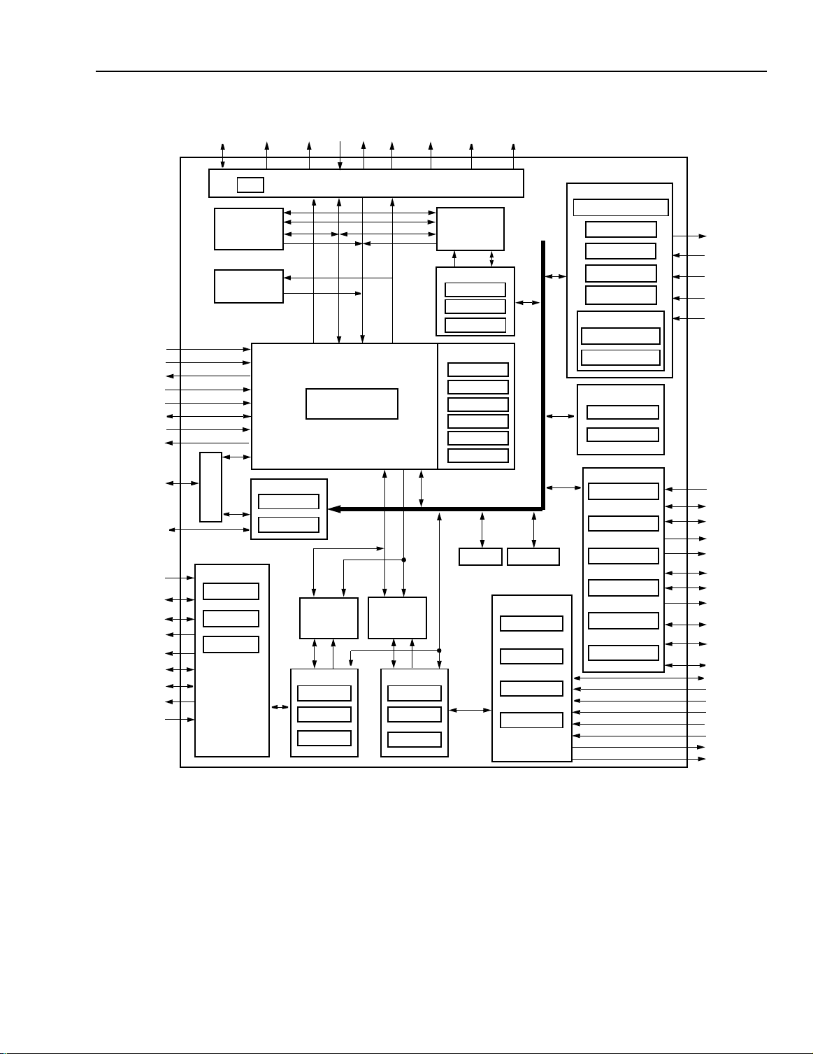
4 Hardware Architecture
The DSP1620 device is a 16-bit, fixed-point, programmable digital signal processor (DSP). The DSP1620
consists of an enhanced DSP1600 core together with
on-chip memory and peripherals. Added architectural
features give the DSP1620 high program efficiency for
signal coding and I/O-intensive applications.
Throughout this manual, all DSP registers directly writable or readable by DSP instructions are printed in lower-case. I/O pins and nonprogram-accessible registers
are upper-case. All register names and DSP instructions are printed in
scriptions.
4.1 DSP1620 Archi tectural Overview
Figure 3 shows a block diagram of the DSP1620. The
following blocks make up this device.
DSP1600 Core
The DSP1600 core is the heart of the DSP1620 chip.
The core contains data and address arithmetic units,
and control for on-chip memory and peripherals. The
core provides support for external memory wait-states
and on-chip dual-port RAM and features vectored interrupts and a trap mechanism. The core is discussed further in Section 4.2.
Dual-Port RAM (DPRAM)
This block contains 30 banks (banks 1—30) of zero
wait-state memory. Each bank consists of 1K 16-bit
words and has separate address and data ports to the
instruction/coefficient and data memory spaces. A program can reference memory from either space. The
DSP1600 core automatically performs the requi red multiplexing. If references to both ports of a single bank are
made simultaneously, the DSP1600 core automati cally
inserts a wait-state and performs the data port access
first, followed by the instruction/coefficient port access.
A program can be downloaded from slow off-chi p memory into DPRAM, and then executed w ithout wait-states.
DPRAM is also useful for improving convolution performance in cases where the coefficients are adaptive.
Since DPRAM can be downloaded through the JTAG
port, full-speed, remote in-circuit emulation is possible.
DPRAM can also be used for downloading self-test
code via the JTAG port.
When the ECCP is active, DPRAM bank 30 is dedic ated
to the ECCP (for storing traceback information) and
cannot be accessed by the core.
boldface
when written in text de-
IORAM
IORAM storage consists of two 1 Kword banks (banks
31 and 32) of on-chip D PRAM that re si des i n the core ’s
internal data memory space. Each bank of IORAM has
two data and two address ports; an IORAM bank can be
shared with the core and a modular I/O unit (MIOU) to
implement a DMA-based I/O system. IORAM supports
concurrent core execution and MIOU I/O processing. If
both the core and MIOU simultaneously access the
same IORAM bank, the DSP1600 cor e automatically inserts a wait-state and performs the MIOU access first,
followed by the core access. MIOU IORAM requests
that do not collide with core IORAM requests do not incur a wait-sta te.
MIOU0 (controls SSIO) is attached to RAM bank 32;
MIOU1 (controls PHIF16) is attached to RAM bank 31.
Portions of IORAM not dedicated to I/O pr ocessing can
be used as general-purpose DPRAM in the data memory map.
Read-Only Memory (ROM)
The DSP1620 contains a 4 Kword boot ROM. The boot
routines are detailed in Section 7.
External Memory Interface (EMI)
The EMI is used to connect the DSP1620 to external
memory and I/O devices. It supports read/write operations from/to instruction/c oef ficient memor y (X memor y
space) and data memory (Y memory space). The
DSP1600 core automatically controls the EMI. Instructions can transparently reference external memory from
either set of internal bus es. A sequencer allows a s ingle
instruction to access both the X and the Y external
memory spaces.
Clock Synthesis
The DSP powers up with a 1X input clock (CKI) as the
source for the processor c lock. An on-chip clock s ynthesizer (PLL) can also be used to generate the system
clock for the DSP that runs at a frequency multiple of the
input clock. The clock synthesizer is deselected and
powered down on reset. For low-power operation, an internally generated slow clock can drive the DSP. If both
the clock synthesizer and the internally generated slow
clock are selected, the slow clock drives the DSP; however, the synthesizer continues to run.
The clock synthesizer and other programmable clock
sources are discussed in Section 4.16. The use of these
programmable clock sources for power management is
discussed in Section 4.17.
14 Lucent Technologies Inc.

Data Sheet
June 1998 DSP1620 Digital Signal Processor
4 Hardware Architecture
Bit Manipulation Unit (BMU)
The BMU extends the DSP1600 core instruction set to
provide more efficient bit operations on accumulators.
The BMU contains logic for barrel shifting, normalization, and bit-field insertion/extr action. The uni t also c ontains a set of 36-bit alternate accumulators. The data in
the alternate accumulators can be shuffled with the data
in the main accumulators. Flags returned by the BMU
are testable by the DSP1600 conditional instructions.
Bit I/O Unit (BIO)
The BIO provides convenient and efficient monitoring
and control of eight individual ly configurable pins. When
configured as outputs, the pins can be individually set,
cleared, or toggled. When configured as inputs, individual pins or combinations of pins can be tested for patterns. Flags returned by the BIO mesh seamlessly with
conditional instructions.
(continued)
Serial I/O Unit (SIO)
The SIO offers an asynchronous, full-duplex, doublebuffered channel that operates at up to 25 Mbits/s (in a
nonmultiprocessor configuration), and easily interfaces
with other Lucent Technologies fixed-point DSPs in a
multiple-processor environment (mul tiprocessor mode).
Commercially available codecs and time-division multiplex (TDM) channels can be interfaced to the SIO with
few, if any, additional components.
In multiprocessor mode, an 8-bit serial protocol channel
can be transmitted in addition to the address of the
called processor. This feature is useful for transmitting
high-level framing information or for error detection and
correction.
Simple Serial I/O Unit (SSIO)
The SSIO offers an asynchronous, full-duplex, doublebuffered external channel that operates up to
25 Mbits/s. Commercially available codecs and timedivision multiplex channels can be interfaced to the
SSIO with few, if any, additional components. The SSIO
external interface is identical to the SIO external interface with the multiprocessor mode functionality and
SADD and SYNC signals deleted.
The SSIO is a DMA peripheral that interfaces di rectly to
the core’s data memory space under the control of
MIOU0.
Lucent Technologies Inc. 15

Data Sheet
DSP1620 Digital Signal Processor June 1998
4 Hardware Architecture
Parallel Host Interface (PHIF16)
The PHIF16 is a passive 16-bit par allel port that can be
configured to interface to either an 8- or 16-bit external
bus containing other Lucent Technologies fixed point
DSPs (e.g., DSP1611, DSP1616, DSP1617, DSP1618,
DSP1620, DSP1627, DSP1628, DSP1629), microprocessors, or peripheral I/O devices. The PHIF16 port
supports either
When operating in the 16-bit external bus configuration,
PHIF16 can be programmed to swap high and low
bytes. When operating in 8-bit external bus configuration, PHIF16 is accessed in either an 8-bit or 16-bit logical mode. In 16-bit mode, the host selects either a high
or low byte access; in 8-bit mode, only the low byte is
accessed.
Additional software-programmable features allow for a
glueless host interface to microprocessors (see
Section 4.10, Parallel Host Interface (PHIF16)).
PHIF16 is a DMA peripheral and interfaces directly to
the core’s data memory space under the control of
MIOU1.
Timer
The timer can be used to provide an interrupt, either single or repetitive, at the expiration of a programmed interval. More than nine orders of magnitude of interval
selection are provided. The timer can be stopped and
restarted at any time.
JTAG and HDS Module
The on-chip Hardware Development System (HDS)
performs instruction breakpointing and branch tracing
at full speed without additional off-chip hardware. Using
the JTAG port, breakpointing is set up, and the trace
history is read back. The port works in conjunction with
the HDS code in the on-chip ROM and the hardware
and software in a remote computer.
A maximum of four hardware breakpoints can be set on
instruction addresses. A counter can be preset with the
number of breakpoints to receive before trapping the
core. Breakpoints can be set in interrupt service routines. Alternately, the counter can be preset with the
number of cache instructions to execute before trapping
the core.
Every time the program branches (rather than executing
the next sequential instruction) the addresses of the instructions executed before and after the branch are
Motorola
or
Intel
(continued)
protocols.
captured in circular memory. This memory contains the
last four pairs of program discontinuities for hardware
tracing.
In systems with multiple processors, the DSPs can be
configured so that any processor reaching a breakpoint
causes all the other processors to be trapped (see
Section 4.3, Interrupts and Trap).
Pin Multiplexing
Upon reset, the vectored interrupt indication signals,
VEC[3:0], are connected to the package pins while
IOBIT[4:7] are disconnected. Setting bit 12, EBIOH, of
ioc
the
pins, and disconnects VEC[3:0]. Note that VEC0 corresponds to IOBIT7, VEC1 corresponds to IOBIT6, VEC2
corresponds to IOBIT5, and VEC3 corresponds to
IOBIT4.
Power Management
Many applications, such as portable cellular terminals,
require programmable sleep modes for power management. There are three different control mechanisms for
achieving low-power operation: the
ister, the STOP pin, and the AWAIT bit in the
ter. The
saving modes by controlling internal clocks and peripheral I/O units. The STOP pin controls the internal processor clock. The AWAIT bit in the
the processor to go into a power-saving standby mode
until an interrupt occurs. The various power management options can be chosen based on power consumption and/or wake-up latency requirements.
Error Correction Coprocessor (ECCP)
The ECCP performs full Viterbi decoding with instructions for MLSE equalization and convolutional decoding. It is designed for 2-tap to 6-tap MLSE equalization
with Euclidean branch metrics and rate 1/1 to 1/6 convolutional decoding using constraining lengths from 2 to
7 with Euclidean or Manhattan branch metrics. Two
variants of soft-decoded symbols, as well as hard-decoded symbols, can be programmed. The ECCP operates in parallel with the DSP1600 core, increasing the
throughput rate. Single instruction Viterbi decoding provides significant code compression required for single
DSP solutions in modern digital cellular applications.
The ECCP is the source of two interrupts and one flag
to the DSP1600 core.
register connects IOBIT[4:7] to the package
powerc
powerc
register configures various power-
alf
control reg-
alf
regis-
register allows
16 Lucent Technologies Inc.
Data Sheet
June 1998 DSP1620 Digital Signal Processor
4 Hardware Architecture
AB[15:0]DB[15:0]
ioc
DPRAM
1K x 16
BANKS 1—29
ROM
4K x 16
CKI
READY
CKO
RSTB
STOP
TRAP
INT[3:0]
IACK
IOBIT[7:4] /
VEC[3:0]
IOBIT[3:0]
DI2
ICK2
ILD2
IBF2
DO2
OCK2
OLD2
OBE2
DOEN2
M
U
X
SSIO
SSIOC*
SSDX(in)*
SSDX(out)*
BIO
sbit
cbit
(continued)
RWN EXM IO EROM ERAMHI ERAMLO
EXTERNAL MEMORY INTERFACE & EMUX
YAB YDB XDB XAB
DSP1600 C OR E
IORAM0
1K x 16
BANK 32
MIOU0
mcmd0
miwp0
morp0
ERAMX
YABYDB
IORAM1
1K x 16
BANK 31
MIOU1
mcmd1
miwp1
morp1
IDB
DPRAM
1K x 16
BANK 30
ECCP
eir
ear
edr
BMU
aa0
aa1
ar0
ar1
ar2
ar3
pllc
powerc
PHIF16
PHIFC*
PSTAT
PDX(in)*
PDX(out)*
BOUNDARY SCAN
†
JTAG
jtag
†
JCON
†
ID
†
BYPASS
HDS
BREAKPOINT
†
TRACE
TIMER
timerc
timer0
SIO
sdx(out)
srta
tdms
sdx(in)
sioc
saddx
†
TDO
TDI
TCK
TMS
TRST
†
DI1
ICK1
ILD1
IBF1
DO1
OCK1
OLD1
OBE1
SYNC1
SADD1
DOEN1
PB[15:0]
PIDS
PODS
PCSN
PBSEL
PSTAT
POBE
PIBF
* These registers are accessible through the MIOU command registers (mcmd0 and mcmd1).
† These registers are accessible through external pins only.
5-4142(F).e
Figure 3. DSP1620 Block Diagram
Lucent Technologies Inc. 17

Data Sheet
DSP1620 Digital Signal Processor June 1998
4 Hardware Architecture
(continued)
Table 2. DSP1620 Block Diagram Legend
Symbol Name
aa<0—1> Alternate Accumulators.
ar<0—3> Auxiliary BMU Registers.
BIO Bit I/O Unit.
BMU Bit Manipulation Unit.
BREAKPOINT Four Instruction Breakpoint Registers.
BYPASS JTAG Bypass Register.
cbit BIO Control Register.
DPRAM Dual-Port Random Access Memory.
ECCP Error Correction Coprocessor.
ear ECCP Address Register.
edr ECCP Data Register.
eir ECCP Instruction Register.
EMUX External Memory Multiplexer.
HDS Hardware Development System.
ID JTAG Device Identification Register.
IDB Internal Data Bus.
ioc I/O Configuration Register.
IORAM0 Bank 32 of Internal Data RAM: Shared with MIOU0.
IORAM1 Bank 31 of Internal Data RAM: Shared with MIOU1.
JCON JTAG Configuration Registers.
JTAG JTAG Test Access Port.
jtag 16-bit Serial/Parallel Register.
MIOU0 Modular I/O Unit 0: Controls SSIO.
mcmd0 MIOU0 Command Register.
miwp0 MIOU0 IORAM 0 Input Data Write Pointer.
morp0 MIOU0 IORAM0 Output Data Read Pointer.
MIOU1 Modular I/O Unit 1: Controls PHIF16.
mcmd1 MIOU1 Command Register.
miwp1 MIOU1 IORAM 1 Input Data Write Pointer.
morp1 MIOU1 IORAM1 Output Data Read Pointer.
MUX Multiplexer.
PHIF16 16-bit Parallel Host Interface.
PDX(in) PHIF16 Input Data Register.
PDX(out) PHIF16 Output Data Register.
PHIFC Parallel Host Interface Control Register: Programmed Through MIOU1.
pllc Phase-Locked Loop Control Register.
powerc Power Control Register.
PSTAT Parallel Host Interface Status Register.
ROM Internal ROM.
saddx SIO Multiprocessor Protocol Register.
sbit BIO Status Register.
sdx(in) Serial Data Transmit Input Register.
sdx(out) Serial Data Transmit Output Register.
SIO Serial I/O Unit.
sioc Serial I/O Control Register.
srta Serial Receive/Transmit Address Register.
SSIO Simple Serial I/O Unit.
SSIOC Serial I/O Control Register for SSIO: Programmed Through MIOU0.
18 Lucent Technologies Inc.
Data Sheet
June 1998 DSP1620 Digital Signal Processor
4 Hardware Architecture
(continued)
Table 2. DSP1620 Block Diagram Legend
Symbol Name
SSDX(in) I/O Data Input Register.
SSDX(out) I/O Data Output Register.
tdms Serial I/O Time-Division Multiplex Signal Control Register.
TIMER Programmable Timer.
timer0 Timer Running Count Register.
timerc Timer Control Register.
TRACE Program Discontinuity Trace Buffer.
XAB Program Memory Address Bus.
XDB Program Memory Data Bus.
YAB D ata Memory Address Bus.
YDB Data Memory Data Bus.
(continued)
Lucent Technologies Inc. 19

Data Sheet
DSP1620 Digital Signal Processor June 1998
4 Hardware Architecture
(continued)
4.2 DSP1600 Core A rc hitectural Overview
Figure 4 shows a block diagram of the DSP1600 core.
System Cache and Control Section (SY S)
This section of the core c ontains a 15-word cac he memory and controls the instruction sequencing. It handles
vectored interrupts and traps, and also provides decoding for registers outside of the DSP1600 core. SYS
stretches the processor cycl e if wai t-states are r equired
(wait-states are programmable for external memory accesses). SYS also sequences downloading via JTAG of
self-test programs to on-chip dual-port RAM.
The cache loop iteration count can be specified at run
time under program control as well as at assembly time.
Data Arithmetic Unit (DAU)
The data arithmetic unit (DAU) contains a 16 x 16-bit
parallel multiplier that generates a full 32-bit product in
one instruction cycle. The product can be accumulated
with one of two 36-bit accumulators. The accumulator
data can be directly loaded from, or stored to memory in
two 16-bit words with optional saturation on overflow.
The arithmetic logic unit (ALU) supports a full set of
arithmetic and logical operations on either 16- or 32-bit
data. A standard set of flags can be tested for conditional ALU operations, branches, and s ubroutine calls. This
procedure allows the processor to perform as a powerful 16- or 32-bit microprocessor for logical and control
applications. The available instruction set is fully compatible with the DSP1627 instruction set. See Section
5.1 for more information on the instruction set.
The user also has access to two additional DAU registers. The
the DAU (see Table 46, psw — Processor Status Word
Register). The arithmetic control register,
to configure some of the features of the D AU (see Table
35) including single-cycle squaring. The
alignment field supports an arithmetic shift left by one
and left or right by two. The
reset.
The counters c0, c1, and c2 are signed, 8 bits wide, and
are used to count events such as the number of times
the program has executed a sequence of code. They
are controlled by the conditional instructions and provide a second convenient method of program looping.
psw
register contains status information from
auc
auc
auc
register is cleared by
, is used
register
Y Space Address Arithmetic Unit (YAAU)
The YAAU supports high-speed, register-indirect, compound, and direct addressing of data (Y) memor y. Four
general-purpose 16-bit registers, r0 to r3, are available
in the YAAU. These registers can be used to supply the
read or write addresses for Y space data. The YAAU
also decodes the 16-bit data memory address and outputs individual memory enables for the data access.
The YAAU can address the thirty-two 1 Kword banks of
on-chip DPRAM/IORAM and a maximum of 128 Kwords
of external storage.
Two 16-bit registers, rb and re, allow zero-overhead
modulo addressing of data for efficient filter implementations. Two 16-bit signed registers, j and k, are used to
hold user-defined postmodification increments. (k is
used only for c ompound address ing.) Fix ed i ncrements
of +1, –1, and +2 are also avail able. Four compound addressing modes are provided to make r ead/wri te operations more efficient.
The YAAU allows direct (or indexed) addressing of data
memory. In direct addressing, the 16-bit base register
ybase
(
dress. The direct data instruction supplies the remaining
5 bits to form an address to Y memory space and also
specifies one of 16 registers for the source or destination.
X Space Address Arithmetic Unit (XAAU)
The XAAU supports high-speed, register-indirect, instruction/coefficient memory addressing with postmodification of the register. The 16-bit pt register is used for
addressing coefficients. The 16-bit signed register i
holds a user-defined postincrement. A fixed postincrement of +1 is also av ailable. Register PC i s the program
counter and is not directly ac cessible by the user. 16-bit
registers pr and pi hold the return address for subroutine calls and interrupts, respectively.
The XAAU decodes the 16-bit instruction/coefficient address and produces enable signals for the appropriate
X memory segment. Addressable instruction/coefficient
segments include on-chip IROM, 30 Kwords on-chip
DPRAM, and 64 Kwords of external storage. The locations of these memory segments depend upon the
memory map selected (see Table 5, Instruction/Coefficient Memory Maps).
) supplies the 11 most significant bits of the ad-
20 Lucent Technologies Inc.
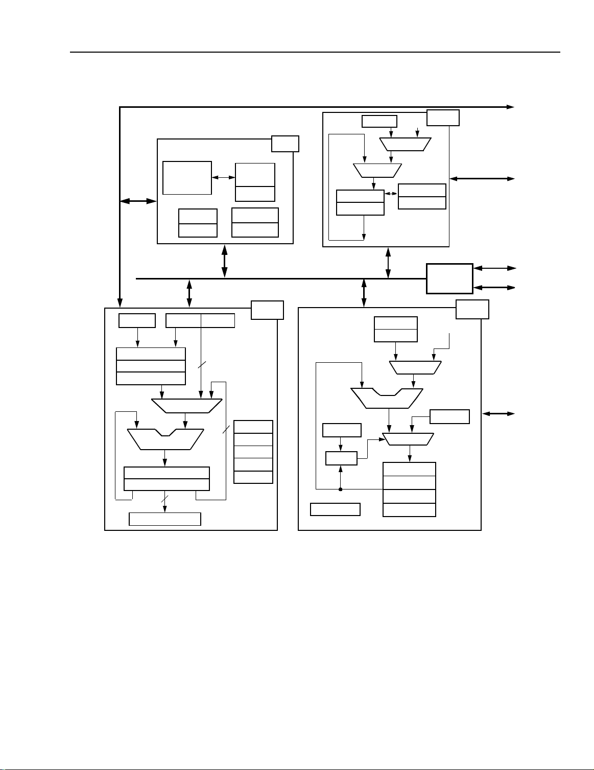
Data Sheet
June 1998 DSP1620 Digital Signal Processor
4 Hardware Architecture
CONTROL
ins (16)
inc (16)
p (32)
yh (16)
yl (16)
32
x (16)
16 x 16 MPY
SHIFT (–2, 0, 1, 2)
(continued)
CACHE
cloop (7)
alf (16)
mwait (16)
DAU
SYS
ADDER
PC (16)
pt (16)
i (16)
j (16)
k (16)
MUX
1
pr (16)
pi (16)
MUX
XAAU
BRIDGE
–1, 0, 1, 2
XDB
XAB
IDB
YDB
YAAU
MUX
ALU/SHIFT
a0 (36)
a1 (36)
16
EXTRACT/SAT
ADDER
36
c0 (8)
c1 (8)
c2 (8)
auc (16)
psw (16)
re (16)
CMP
ybase (16)
Figure 4. DSP1600 Core Block Diagram
YAB
rb (16)
MUX
r0 (16)
r1 (16)
r2 (16)
r3 (16)
5-1741(F).b
Lucent Technologies Inc. 21

Data Sheet
DSP1620 Digital Signal Processor June 1998
4 Hardware Architecture
(continued)
Table 3. DSP1600 Core Block Diagram Legend
Symbol Name
16 x 16 MPY 16-bit x 16-bit Multiplier.
a0—a1
Accumulators 0 and 1 (16-bit halves specified as a0,
alf AWAIT, LOWPR, F lags.
ALU/SHIFT Arithmetic Logic Unit/Shifter.
auc Arithmetic Unit Control.
c0—c2 Counters 0—2.
cloop Cache Loop Count.
CMP Comparator.
DAU Data Arithmetic Unit.
EXTRACT/SAT Extract/Saturate.
i Increment Register for the X Address Space.
IDB Internal Data Bus.
inc Interrupt Control Register.
ins Interrupt Status Register.
j Increment Register for the Y Address Space.
k Increment Register for the Y Address Space.
MUX Multiplexer.
mwait External Memory Wait-States Register.
p Product Register.
PC Program Counter.
pi Pr ogram Interrupt Return Register.
pr Program Return Register.
psw Pr o cessor Status W o rd.
pt X Address Space Pointer.
r0—r3 Y Address Space Pointers.
rb Modulo Addressing Register (begin address).
re Modulo Addressing Register (end address).
SYS System Cache and Control Section.
x Multiplier Input Register.
XAAU X Space Add re ss Arithmetic Un it.
XAB X Space Address Bus.
XDB X Space Data Bus.
y DAU Register.
YAAU Y Space Add re ss Arithmetic Un it.
YAB Y Space Address Bus.
YDB Y Space Data Bus.
ybase Direct Addressing Base Register.
* F3 ALU instructions with immediates require specifying the high half of the accumulators as
a0l, a1
a0h
and
, and
a1h
*
a1l
.
)
.
22 Lucent Technologies Inc.

Data Sheet
June 1998 DSP1620 Digital Signal Processor
4 Hardware Architecture
(continued)
4.3 Interrupts and Trap
The DSP1620 supports prioritized, vectored interrupts
and a trap. The device has eleven internal hardware interrupt sources and four external interrupt pins. Additionally, there is a trap pin and a trap signal from the
hardware development system (HDS). A software i nterrupt is available through the
instruction is reserved for use by the HDS. Each of
these sources of interrupt and trap has a unique vector
address and priority assigned to it.
The software interrupt and the traps are always enabled
and do not have a corresponding bit in the
Other vectored interrupts are enabled in the
(see Table 39, inc — Interrupt Control Register) and
monitored in the
rupt Status Register). When the DSP1620 goes into an
interrupt or trap service routine, the IACK pin is asserted. In addition, pins VEC[3:0] encode which interrupt/
trap is being serviced. Table 4 details the encoding
used for VEC[3:0].
The DSP1620 WAKEUP interrupt is a new source of
core interrupt. WAKEUP is triggered by the logical OR
of the PHIF16 input buffer full flag and the SSIO input
buffer full flag. The purpose of this interrupt is to reactivate sleeping MIOUs (
peripheral input processing.
Interruptibility
Vectored interrupts are serviced only after the execution
of an interruptible instruction. If more than one
vectored interrupt is asserted at the same time, the interrupts are serviced sequentially according to their assigned priorities. S ee Table 4 for the priorities assigned
to the vectored interrupts. Interrupt service routines,
branch and conditional branch instructions, cache
loops, and instructions that only decrement one of the
RAM pointers, r0 to r3 (e.g., *
ible.
A trap is similar to an interr upt, but it gains control of the
processor by branching to the trap service routine even
when the current instruction i s noninterruptible. It might
not be possible to return to normal ins truction execution
from the trap service routine because the machine state
cannot always be saved. In particular, program execution cannot be continued from a trapped cache loop or
interrupt service routine. While in a trap service routine,
another trap is ignored.
ins
register (see Table 40, ins — Inter-
icall
instruction. The
ins
alf
AWAIT bit set) and resume
r3
− −
), are not interrupt-
register.
inc
register
icall
When set to 1, the status bits in the
that an interrupt has occurred. The processor must
reach an interruptible state (completion of an interruptible instruction) before an enabled vectored interrupt is
acted on. An interrupt is not serviced if it is not enabled.
Polled interrupt service can be implemented by disabling the interrupt in the
ins
the
register for the expected event.
Vectored Interrupts
Tables 39 and 40 show the
1 written to any bit of
sociated interrupt. If the bit is cleared to a logic 0, the interrupt is masked. Note that neither the software
interrupt nor traps can be masked.
The occurrence of an interrupt that is not masked causes the program execution to transfer to the memory location pointed to by that interrupt's vector address,
assuming no other interrupt is being serviced (see Ta-
ble 4). The occurrence of an interrupt that is masked
causes no automatic processor action, but sets the c orresponding status bit in the
terrupt occurs, it is latched in the
interrupt is not taken. When unlatched, this latched interrupt initiates automatic processor interrupt action.
See the
Manual for a more detailed description of the interrupts.
Signaling Interrupt Service Status
Five pins of DSP1620 are devoted to signaling interr upt
service status. The IACK pin goes high while any interrupt or user trap is being serviced, and goes low when
the ireturn instruction from the servic e routine is issued.
Four pins, VEC[3:0], carry a code indicating which of the
interrupts or trap is being serviced. Table 4 contains the
encodings used by each interrupt.
Traps due to HDS breakpoints have no effect on either
the IACK or VEC[3:0] pins. Instead, they show the interrupt state or interrupt source of the DSP when the trap
occurred.
DSP1620 Digital Signal Processor
inc
inc
inc
enables (or unmasks) the as-
ins
ins
register indicate
register and then polling
ins
and
registers. A logi c
register. If a masked in-
ins
register, but the
Information
Lucent Technologies Inc. 23

Data Sheet
DSP1620 Digital Signal Processor June 1998
4 Hardware Architecture
Table 4. Interrupt Vectors
Source Vector Priority VEC[3:0] Issued by
No Interrupt — — 0x0 —
Software Interrupt 0x2 1 0x1 icall
INT0 0x1 2 0x2 INT0 pin
JINT 0x42 3 0x8 jtag pin
INT1 0x4 4 0x9 INT1 pin
INT2 0x8 5 0xa INT2 pin
INT3 0xc 6 0xb INT3 pin
TIME 0x10 7 0xc timer
MIBF0 0x14 8 0xd MIOU0 (SSIO )
MOBE0 0x18 9 0xe MIOU0 (SSIO)
WAKEUP 0x1c 10 0x0 SSIO or PHIF16 input buffer full
EREADY 0x20 11 0x1 ECCP ready
EOVF 0x24 12 0x2 ECCP overflow
IBF 0x2 c 14 0x3 SIO in
OBE 0x30 15 0x4 SIO out
MIBF1 0x34 16 0x5 MIOU1 (PHIF16)
MOBE1 0x38 17 0x6 MIOU1 (PHIF16)
TRAP from HDS 0x3 18
TRAP from User 0x46 19 = highest 0x7 pin
* Traps due to HDS breakpoints have no effect on VEC[3:0] pins.
(continued)
—*
breakpoint, jtag, or pin
Clearing Interrupts
MIOU-reported SSIO and PHIF16 interrupts (MIBF0, MOBE0, MIBF1, MOBE1) are cleared by writing the reporting
MIOU’s command register with the appropriate length update command. See Section 4.8.
The SIO interrupts (IBF, OBE) are cleared one instruction cycle after reading or writing, as appropriate, the serial
data registers
nop
tion (
terrupt service routine (via
reported following an ireturn.
The JTAG interrupt (JINT) is cleared by reading the
Eight of the vectored interrupts can be cleared by writing to the
INT3, TIME, EREADY, EOVF, or WAKEUP bits in the
cleared to a logic 0. The status bit for these vectored interrupts is also cleared when the ireturn instruction is executed, leaving set any other vectored interrupts that are pending.
sdx
(in), and
or other) follows the
sdx
(out). To account for this latency, the programmer shoul d ensure that a single i nstruc-
sdx
read/write instruction before examining the
ireturn
). This ensures that stale flags are not read or that an erroneous interrupt is not
jtag
register.
ins
register. Writing a 1 to the INT0, INT1, INT2,
ins
will cause the corresponding interrupt status bit to be
ins
register or prior to leaving an in-
24 Lucent Technologies Inc.

Data Sheet
June 1998 DSP1620 Digital Signal Processor
4 Hardware Architecture
Traps
The TRAP pin of the DSP1620 is a bidirectional signal.
At reset, it is configured as an input to the processor.
Asserting the TRAP pin forces a user trap. Once the
trap pin is asserted, it must remain asserted until
VEC[3:0] is 0xd (acknowledgment). The trap mechanism is used for two purposes: by an application to rapidly gain control of the processor for asynchronous timecritical event handling (typical ly for catastrophic error recovery). It is also used by the HDS for breakpointing
and gaining control of the processor. Separate vectors
are provided for the user trap (0x46) and the HDS trap
(0x3). Traps are not maskable.
A trap has four cycles of latency. At most, two instructions execute from the time the trap is received at the
pin to when it gai ns control. An instruction that is exec uting when a trap occurs is allowed to complete before the
trap service routine is entered. (Note that the instruction
could be lengthened by wait-states.) During normal program execution, the pi register contains either the address of the next instruction (two-cycle instruction
executing) or the address following the next instruction
(one-cycle instruction executing). In an interrupt service
routine, pi contains the interrupt return address. When
a trap occurs during an interrupt servi ce routine, the value of the pi register is overwritten. Specifically, it is not
possible to return to an interrupt service routine from a
user trap (0x46) service routine. Also, continuing program execution when a trap occurs during a c ache loop
is not possible.
The HDS trap causes circuitry to force the program
memory map to XMAP1 (with on-chip ROM starting at
address 0x0) when the trap is taken. The previous
memory map is restored when the trap service routine
exits by issuing an i return. The map is forced to XMA P1
because the HDS code resides in the on-chip ROM.
(continued)
Wait for Interrupt (Standby or Sleep Mode)
The DSP1620 has a power-saving standby mode in
which the internal processor clock stretches indefinitely
until the core receives an interrupt or trap request. A
minimum amount of core circuitry remains active in
order to process the incoming interrupt. The clocks to
the peripherals are unaffected and the peripherals continue to operated during standby mode. The program
places the core in standby mode by setting the AWAIT
bit (bit 15) of the
AWAIT bit is set, one additional instruction is executed
before the standby mode is entered. When an interrupt
occurs, core hardware resets AWAIT, and normal core
processing is resumed.
The MIOUs remain operational even in standby mode.
Their clocks remains running and they continue any
DMA activity.
nop
Two
AWAIT bit is set. The first
before sleeping; the second is executed after the interrupt signal awakens the DSP and before the interrupt
service routine is executed.
The AWAIT bit should be set from within the cache if the
code that is executing resides in external program
memory where more than one wait-state has been programmed. This ensures that an interrupt does not disturb the device from completely entering the sleep state.
For additional power savings, in addition to setting
the value 0x8000, set
erc
shuts down the timer and prescaler (see Table 54 and
Table 41).
Power consumption can be further reduced by by activating other available low-power modes. See Power
Management beginning on page 71 for information on
these other modes.
instructions should be programmed after the
to the value 0x0040. This holds the CKO pin low and
alf
register (
alf
= 0x8000). After the
nop
(one cycle) is executed
ioc
to the value 0x0180 and
alf
to
tim-
Using the Lucent Technologies development tools, the
TRAP pin can be configured to be an output or an input
vectoring to address 0x3. In a multiprocessor environment, the TRAP pins of all the DSPs present can be tied
together. During HDS operations, one DSP is selected
by the host software to be the master. The master processor's TRAP pin is configured to be an output. The
TRAP pins of the slave processors are configured as inputs. When the master processor reaches a breakpoint,
the master's TRAP pin is asserted. The slave processors respond to their TRAP input by beginning to execute the HDS code.
Lucent Technologies Inc. 25

Data Sheet
DSP1620 Digital Signal Processor June 1998
4 Hardware Architecture
(continued)
4.4 Memory Maps and Wait-States
The DSP1600 core implements a modified Harvard architecture that has separate on-chip 16-bit address and
data buses for the instruction/coefficient (X) and data
(Y) memory spaces. The DSP1620 provides a multiplexed external bus that accesses external RAM
(ERAM), ROM (EROM), and memory-mapped I/O
space (I/O). Programmable wait-states are provided for
external accesses.
Both the instruction/coefficient memory space and data
memory space are configurable to provide application
flexibility.
Table 5 shows the DSP1620 instruction/coefficient
memory space maps including the values for the external ROM enable pin (EROM) and address range of the
external memory interface address bus (AB).
Table 6 shows the DSP1620 data memory space in-
cluding values for the EROM, ERAMHI, ERAMLO,
ERAMX, IO, and AB external memory interface pins.
Instruction/Coefficient Memory Map Selection
Three parameters are used to select the active instruction/coefficient memory map: LOWPR, EXTROM, and
EXM.
The LOWPR bit of the
tomatically at reset. LOWPR controls the starting address of the thirty 1K banks of DPRAM. If LOWPR is
low, DPRAM begins at address 0x8000. If LOWPR is
high, DPRAM begins at address 0x0. IROM is not visible when LOWPR is asserted.
When LOWPR is asserted, the EXTROM bit of the
register determines which 32K segment of a possible
64K EROM physical address s pace is vis ible to the programmer. If EXTROM is asserted, physi cal EROM locations 0x0—0x7FFF are visible in the logical address
space 0x8000—0xFFFF. If EXTROM is deasserted,
physical EROM locations 0x8000—0xFFFF are visible
in the logical address space 0x8000—0xFFFF.
If LOWPR is deasserted, the value of the EXM pin at reset determines whether the internal 4 Kwords ROM
(IROM) or EROM locations 0x0—0x7FFF are addressable in the address range 0x0—0x7FFF.
The Lucent Technologies development system tools,
together with the on-chip HDS circuitry and the JTAG
port, can independently set the memory map. Specifically, during an HDS trap, the memory map is forced to
XMAP1. The user's map selection is r estored when the
trap service routine has completed execution.
alf
register is initialized to 0 au-
ioc
26 Lucent Technologies Inc.

Data Sheet
June 1998 DSP1620 Digital Signal Processor
4 Hardware Architecture
(continued)
XMAP1
XMAP1 has IROM starting at 0x0 and 30 Kwords of DPRAM starting at 0x8000. XMAP1 is established if DSP1620
has EXM low at reset and the LOWPR parameter is programmed to zero. XMAP1 is also used during an HDS trap.
XMAP2
XMAP2 has 32 Kwords of external ROM (physical EROM addresses 0x0000—0x7FFF) starting at address 0x0. A s
in XMAP1, 30 Kwords of DPRAM begins at address 0x8000.
XMAP3
XMAP3 has 30 Kwords of DPRAM starting at address 0x0. 32 Kwords of EROM (physical EROM addresses
0x8000—0xFFFF) storage begins at 0x8000.
XMAP4
XMAP4 has 30 Kwords of DPRAM starting at address 0x0. 32 Kwords of EROM (physical EROM addresses
0x0000—0x7FFF) storage begins at 0x8000.
Table 5. Instruction/Coefficient Memory Maps
*
†
EXTROM = X
‡
LOWPR = 0
XMAP2
EXM = 1
EXM = X
†
EXTROM = 0
LOWPR = 1
XMAP3
§
EXM = X
§
EXTROM = 1
LOWPR = 1
XMAP4
X Address
XMAP1
EXM = 0
EXTROM = X
LOWPR = 0
0x0000—0x0FFF
0x1000—0x77FF
0x7800—0x7FFF
0x8000—0xF7FF
0xF800—0xFFFF
* MAP1 is set automatically during an HDS trap. The user-selected map is restored at the end.
† EXTROM is a don’ t care when LOWPR is d easser ted.
‡LOWPR is
memo ry map.
§ EXM is a don’t care when LOWPR is asserted.
alf
regis ter bit 14. The Lucent Technologi es development s ystem tool s c an i ndependently se t the
IROM
(4K)
EROM = 1
RESERVED
EROM
(32K)
EROM = 0
AB = 0x0000—
0x7FFF
DPRAM
(30K)
EROM = 1
DPRAM
(30K)
EROM = 1
RESERVED RESERVED
DPRAM
(30K)
EROM = 1
EROM = 1
RESERVED RESERVED
EROM
(32K)
EROM = 0
AB = 0x8000—
0xFFFF
EROM = 0
AB = 0x0000—
0x7FFF
DPRAM
(30K)
EROM
(32K)
Lucent Technologies Inc. 27

Data Sheet
DSP1620 Digital Signal Processor June 1998
4 Hardware Architecture
Boot from External ROM
After RSTB goes from low to high, the DSP1620 comes
out of reset and fetches an instruction from address
zero of the instruction/coefficient space. The physical
location of address zero is determined by the memory
map in effect. If EXM is high at the rising edge of RSTB,
XMAP2 is selected. XMAP2 has EROM at location zero;
thus, program execution begins from external memory.
If EXM is high and INT1 is low when RSTB rises, the
mwait
register defaults to 15 wai t-states for all external
memory segments. If INT1 is high, the
defaults to 0 wait-states.
Data Memory Map Selection
Data memory map selection is based upon the value of
the EXTROM and WEROM
YMAP1
In YMAP1, the programmer can access 32 Kwords of
DPRAM (logical address 0x0000—0x7FFF), and the
most significant half of the 64 Kwords physical ERAM
space.
(continued)
ioc
register bits.
mwait
register
YMAP2
In YMAP2, the programmer can access 32 Kwords of
DPRAM (logical address 0x0000—0x7FFF), and the
least significant half of the 64 Kwords physical ERAM
space.
YMAP3
In YMAP3, the programmer can access 32 Kwords of
DPRAM (logical address 0x0000—0x7FFF), and the
most significant half of the 64 Kwords physical EROM
space.
YMAP4
In YMAP4, the programmer can access 32 Kwords of
DPRAM (logical address 0x0000—0x7FFF), and the
least significant half of the 64 Kwords physical EROM
space.
28 Lucent Technologies Inc.
 Loading...